International Journal of Scientific & Engineering Research, Volume 5, Issue 5, May-2014 1425
ISSN 2229-5518
Simulation of DSTATCOM for Power Quality Enhancement in Distribution Networks under Various Fault Condition
Saeed Ebrahimi Shah Gholi, Hadi Zayandehroodi, Mohammad Shabani Poor, Javad Alihosseini Hamid Pakari
Abstract: In this project Flexible Alternating Current Transmission Systems (FACTs) use Power electronic devices and methods to control the high-voltage side of the network for improving the flow of power. Custom Power Devices are mainly for low-voltage distribution, and improving poor quality of power and reliability of supply affecting entities such as factories, offices and homes. The quality of Power and Reliability are becoming important issues for critical and sensitive loads after introducing the term of Custom Power. In general due to the structure of Custom Power Devices is classified into three categories such as Dynamic Voltage Restorer (DVR), Distribution STATCOM (DSTATC0M) and Unified Power Quality Compensator (UPQC).These are existing methods are used to improving quality of Power and reliability of supply and also mitigate all type of faults. In this Project we are using DSTATCOM because it has more reliable, fast response among those categories under Custom Power Devices. DSTATCOM is mainly used to mitigate all types of fault, intelligently (such as Single Line to Ground (SLG) fault and Double Phase to Ground (DPG) fault and three- phase fault). Due to the fast response of DSTATCOM makes it the efficient solution for enhancing the power quality of the distribution system.
—————————— ——————————
hunt Connected Controllers at distribution and transmission levels usually fall under two catogories - Static Synchronous Generators (SSG) and Static VAr Compensators (SVC). A Static Synchronous Generator (SSG) is defined by IEEE as a self-commutated switching power converter supplied from from an appropriate electric energy source and operated to produce a set of adjustable multiphase voltages , which may be coupled to an ac power system for the purpose of exchanging independently controllable real and reactive power. When the active energy source (usually battery bank, Superconducting Magnetic Energy Storage etc) is dispensed with and replaced by a DC Capacitor which cannot absorb or deliver real power except for short durations the SVG becomes a Static Synchronous
————————————————
Compensator (STATCOM) [1,2]. STATCOM has no long
term energy support in the DC Side and cannot exchange real power with the ac system; however it can exchange reactive power. Also, in principle, it can exchange harmonic power too. But when a STATCOM is designed to handle reactive power and harmonic currents together it gets a new name – Shunt Active Power Filter. So a STATCOM handles only fundamental reactive power exchange with the ac system [9].
STATCOMs are employed at distribution and transmission levels – though for different purposes. When a STATCOM is employed at the distribution level or at the load end for power factor improvement and voltage regulation alone it is called DSTATCOM. When it is used to do harmonic filtering in addition or exclusively it is called Active Power Filter. In the transmission system STATCOMs handle only fundamental reactive power and provide voltage support to buses. In addition STATCOMs in transmission system are also used to modulate bus voltages duting transient and dynamic disturbances in order to improve transient stability margins and to damp dynamic oscillations. IEEE defines the second kind of Shunt Connected Controller called Static VAr Compensator (SVC) as a shunt connected static var generator or absorber whose output is adjusted to exchange capacitive or inductive current so as to maintain or control specific parameters of the electrical power system (typically bus voltage) [2]. Thyristor-switched or thyristor-controlled capacitors/inductors and combinations of such equipment with fixed capacitors and inductors come under this.This has been covered in an earlier lecture and this lecture focusses on STACOMs at distribution and transmission levels. PWM Voltage
IJSER © 2014 http://www.ijser.org
International Journal of Scientific & Engineering Research, Volume 5, Issue 5, May-2014 1426
ISSN 2229-5518
Source Inverter based Static VAr Compensators (referred to as SVC here onwards) began to be considered a viable alternative to the existing passive shunt compensators and Thyristor Controlled Reactor (TCR) based compensators from mid-eighties onwards. The disadvantages of capacitor/inductor compensation are well known. TCRs could overcome many of the disadvantages of passive compensators. However they suffered from two major disadvantages; namely slow response to a VAr command and injection of considerable amount of harmonic currents into the power system which had to be cancelled by special transformers and filtered by heavy passive filters. It became clear in the early eighties that apart from the mundane job of pumping lagging/leading VArs into the power system at chosen points ,VAr generators can assist in enhancing stability of the power system during large signal and small signal disturbances if only they were faster in the time domain. Also, they can provide reactive support against a fluctuating load to maintain the bus voltage regulation and to reduce flicker problems, provide reactive support to control bus voltages against sag and swell conditions and provide reactive support to correct the voltage unbalance in the source – if only they were fast enough. PWM STATCOMs covered in this lecture are capable of delivering lagging/leading VArs to a load or to a bus in the power system in a rapidly controlled manner. High Power STATCOMs of this type essentially consist of a three phase PWM Inverter using GTOs, Thrusters or IGBTs, a D.C. side capacitor which provides the D.C. voltage required by the inverter, filter components to filter out the high frequency components of inverter output voltage, a link inductor which links the inverter output to the a.c supply side, interface magnetic (if required) and the related control blocks. The Inverter generates a three-phase voltage, which is synchronized with the a.c supply, from the D.C. side capacitor and the link inductance links up this voltage to the a.c source. The current drawn by the Inverter from the a.c supply is controlled to be mainly reactive (leading or lagging as per requirement) with a small active component needed to supply the losses in the Inverter and Link Inductor (and in the magnetics, if any).The D.C. side capacitor voltage is maintained constant ( or allowed to vary with a definite relationship maintained between its value and the reactive power to be delivered by the Inverter) by controlling this small active current component. The currents are controlled indirectly by controlling the phase angle of Inverter output Voltage with respect to the a.c side source voltage in the "Synchronous Link Based Control Scheme" whereas they are controlled directly by current feedback in the case of "Current Controlled Scheme". In the latter case the Inverter will be a Current Regulated one, i.e. its switches are controlled in such a way that the Inverter delivers a commanded current at its output rather than a commanded voltage (the voltage required to see that the commanded current flows out of
Inverter will automatically be synthesized by the Inverter).Current Control Scheme results in a very fast STATCOM which can adjust its reactive output within tens of microseconds of a sudden change in the reactive demand [9].
However, current control schemes will require high frequency switching in the Inverter – switching frequencies which are so high that low frequency devices like thyristors and GTOs are ruled out. Hence they have to be based on MOSFETS or IGBTS.The latter seems to be the current choice with its high voltage and high current rating availability with low conduction losses. However, at present, they are limited to applications in the low voltage systems (400V,1.1kV etc) and at distribution power level rather than transmission and sub- transmission power levels. This is because of the limited maximum voltage/current ratings available in a single device/module. Thus DSTATCOMs use IGBTs and they usually employ the standard two-level 3 limb , three phase inverter with voltage and current levels adjusted by ratio of transformation in the coupling transformer At the most they may use series-parallel device structures to increase voltage and current rating of the switches. However multi-pulse or multi-level or cascaded inverters are rarely required in Distribution STATCOMs. High frequency switching is possible due to the device being IGBT and ‘Current Regulated Mode of Operation" is employed to force the inverter to deliver set values of currents into the ac system. When it comes to transmission/sub-transmission level GTOs are the preferred devices and they can take switching frequencies below 1-3 kHz. Hence, at these levels, STATCOMs are made with the Synchronous Link Control Scheme which gates the Inverter to deliver a voltage output (rather than a regulated current).This kind of Inverter operation makes it possible to implement one of the many specialized PWM switching schemes aimed at minimizing the switching frequency while keeping acceptable level of harmonic content in the Inverter output.The device used i.e GTO dictates a low switching frequency.But the inverter should not inject harmonics into the ac system. And the voltages and currents to be handled are large.These three factors together make two- level three-limb three-phase inverter under SPWM impossible in STATCOM. The solution usually lies in Multi-Pulse Inverters, Muti-Level Inverters or Multi- Level Cascaded Inverters [9]. These types are better controlled as voltage sources than current sources.Thus
‘Synchronous Link Phase Angle Control Scheme’ or
‘Predictive Indirect Current Control’ are the control choices. Summing up, STATCOMs are fast responding generators of reactive power with leading VAr/lagging VAr capability which can provide steady state reactive compensation as well as dynamic compensation during power system transients,sags, swells,flicker etc. Thereby they can contribute significantly to enhancement of Power Quality. High Power STATCOMs in the
IJSER © 2014 http://www.ijser.org
International Journal of Scientific & Engineering Research, Volume 5, Issue 5, May-2014 1427
ISSN 2229-5518
transmission system are usually made with devices of low switching frequency capability (GTO’s) and hence need special PWM patterns to optimize switching behavior. Such STATCOMs use Synchronous Link principle in the control blocks. DSTATCOMs use high speed switching levels, simple inverter structures and high frequency PWM or Hysteresis Control to function as Current Regulated Sources whereas transmission system STATCOMs use multi-pulse or multi-level inverters using GTO’s and function as controlled voltage sources with controllable phase and use Synchronous Link Control principle.
In a synchronous link where two a.c sources of same frequency are connected together by means of a link inductor, active power flows from the leading bus to the lagging one and reactive power flows from the source with higher voltage magnitude to the one with lower voltage magnitude. The active power flow is almost entirely decided by the lead angle whereas the reactive flow is almost entirely decided by the difference in voltage magnitudes provided the inductor is loss free ,the lead angle is small (less than 15 degrees) and the voltage magnitude difference is small(less than 0.1 p.u) . The situation changes slightly if the link contains resistance. If two sources V1 with a phase angle of µ and V2 with a phase angle of 0 are connected together by means of an inductive link of impedance (R+jX) ohms and if the active power flowing into the source V2 is constrained to be zero (because this represents the STATCOM situation) the power delivered by the source V1 (which will not be zero and it will be equal to the power absorbed by the resistance in the link ) and the reactive power delivered to the link by the source V2 will be given by the following relations (after a little algebra along with the assumptions that µ is small and R << X ).
Active Power Delivered by
P = (V12/R) µ2 Watts (1)
Reactive Power Delivered by
Q = (V1V2/R) µ VArs (2)
Also
Q = V2(V2-V1)/X VArs (3)
Where the powers are for a phase and voltages have
phase values. These relations can be used upto about 20 degrees for µ .Active Power drawn from the source V1 is independent of sign of phase angle (only V1 can supply losses in R because of the zero active power constraint at V2) whereas the reactive power delivered by V2 is directly proportional to the phase angle. In the STATCOM context, the source V1 is the power system voltage at the bus where the STATCOM is connected,V2 is the a.c voltage generated by the Inverter in the
STATCOM, R is the total loss resistance in the link comprising the winding losses in the link inductor,interface magnetics and the inverter switches and snubbers etc. This shows that the relative phase angle is linearly related to the voltage magnitude difference (for small differences) and hence the reactive power delivered by V2 is proportional to the voltage magnitude difference. Thus Q is proportional to µ or equivalently to (V2-V1). Both points of view will be useful later to understand the two different ways in which this STATCOM can be controlled. In the STATCOM, the required a.c voltage source V2 is generated by inverting the D.C. voltage, which is assumed available across the capacitor in the D.C. side. But if the active power which goes into the inverter from the mains is kept zero, the initially charged capacitor will soon discharge down to zero due to active power losses in the Inverter which the D.C. side will have to supply. The D.C. side voltage will remain constant (or at least controlled) if the power drawn from mains is just enough to supply all the losses which take place everywhere due to the flow of demanded reactive current.
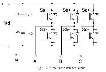
A Three-Phase Inverter using IGBTs is shown in Fig.1.In certain cases the neutral wire may not be present and the D.C. side capacitor may be a single one. However, for the purpose of explanation, a neutral point may always be imagined. With this the three phase Inverter becomes three separate single-phase half bridge Inverters sharing the same D.C. source. Bipolar and unipolar PWM schemes using a triangular carrier frequency was discussed in another lecture ([4] page 70-72) in the context of single-phase full bridge converters. Much of the same is applicable here too except that only bipolar PWM is possible for a half bridge topology since no combination of switching patterns for the upper and lower switches of a half bridge can apply zero potential at the load point. Bipolar PWM using a triangular carrier and sinusoidal
IJSER © 2014 http://www.ijser.org
International Journal of Scientific & Engineering Research, Volume 5, Issue 5, May-2014 1428
ISSN 2229-5518
modulating voltage can be applied here with the modulating waves of the three half bridge sections forming a balanced three phase signal set. However,the switching frequency required in Sinusoidal Pulse Width Modulation using triangular Carrier to achieve reduction in output harmonics is usually excessive as far as high power devices like GTOs are concerned. Hence, programmed harmonic elimination techniques is preferred at high power levels.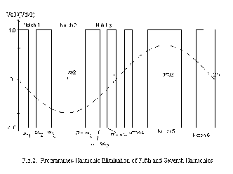
Like in any other PWM scheme, +Vd/2 and –Vd/2 pulses are applied across the load in the programmed harmonic elimination technique also. But in this scheme the position and duration of these pulses are pre-calculated off-line in such a way that (i) certain chosen harmonics are completely eliminated completely in the output and (ii) the fundamental component of the output has a desired value. By a general formulation of Fourier series coefficients of a pulse wave it is possible to derive a set of equations involving angle positions of the positive and negative pulses to satisfy the conditions on elimination of chosen harmonics and on the fundamental amplitude. The maximum possible amplitude will be available when the output is a full square wave (i.e. no harmonics are eliminated) and will be 1.275(Vd/2).But when harmonics are to be eliminated it is not possible to reach this value of fundamental voltage. For every selection of harmonics to be eliminated there exists a maximum value the fundamental component can have and it will be less than
1.275(Vd/2).For example ,it is 1.188(Vd/2) for a scheme
where fifth and seventh harmonics are eliminated.Fig.2 shows the normalized pulse pattern which appears at A phase output when fifth and seventh harmonics are sought to be eliminated. The switching frequency of each will be 350Hz with this pattern. The equations which yield the angular positions for a chosen elimination format and fundamental amplitude is transcendental algebraic in nature and require numerical techniques for solution. Moreover for the same harmonic elimination format the switching angles will vary with the fundamental amplitude desired;and the variation can be highly nonlinear. See Fig.3.The nature of equations make
an on-line implementation of pattern generation very difficult. In addition, the nonlinear angular position variation with changes in the desired fundamental component makes it difficult to generate the PWM pattern in real time by analog/digital logic. However, it is possible to implement this scheme using micro processors/controllers and EPROMs.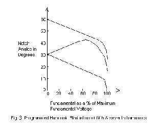
A sinusoidal reference wave at frequency equal to the desired output frequency of the Inverter is frequency multiplied in a PLL system. The square wave from VCO of PLL is used to clock a UP/DOWN counter. The counter output is used as address bytes of an EPROM which has the required switching pattern at that instant written in it(by off-line computation and EPROM programming) [8]. The EPROM has patterns stored for various quantised values of fundamental amplitude. The control signal which sets the fundamental amplitude is A/D converted and the code is used to decide the range of EPROM memory locations to be read out by the counter output. Once in a fundamental cycle the counter is forcibly reset (at zero crossing of reference sine wave usually), to avoid subharmonic components in the output due to jitter in the PLL and other similar errors everywhere. Note that it is possible to shift the phase of the fundamental component of Inverter output with respect to reference sine by shifting the counter reset point with respect to the zero crossing point of reference sine. A three-phase pattern can be similarly generated. However, large memory may be required for fine control of output voltage fundamental value [8,9].
IJSER © 2014 http://www.ijser.org
International Journal of Scientific & Engineering Research, Volume 5, Issue 5, May-2014 1429
ISSN 2229-5518
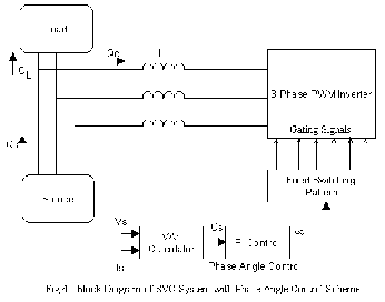
Fig.4. shows a DSTATCOM configured to keep the reactive power delivered by the Source at a zero value as long as the reactive demand from the load is within the DSTATCOM rating. Thus, the p.f of the Source will be maintained at unity under steady state conditions by the DSTATCOM [5]. The control of DSTATCOM reactive power is by pure µ control and the D.C. bus voltage is allowed to vary. This scheme, though somewhat slow, results in simplified control hardware. The source side voltages and currents are sensed and the reactive power is calculated by analog/pulse circuitry. This calculated value is compared with the desired value (usually zero) and the error is processed in a proportional-integral controller. The error output decides the phase shift needed in the inverter output in order to develop the required D.C. bus voltage such that the inverter output voltage magnitude will be sufficient to make the Inverter deliver the VArs required by the load. The Inverter is gated by a fixed PWM pattern optimised for eliminating chosen harmonics (usually fifth, seventh, eleventh etc; triplen harmonics need not be eliminated since they do not result in current flows in a three wire system). The needed PWM pattern is stored in an EPROM and is read out using the scheme described in the last section. This is by far the most popular scheme used in high power STATCOMs. The open loop dynamics of the STATCOM features a third order transfer function (for small signals) between µ and Qc, the reactive power delivered by the Inverter.The transfer function has a pair of complex zeros, a real pole and a pair complex poles. Various research workers have derived the following transfer function for the STATCOM.
Qc (s)/µ (s) = N(s)/D(s) where
N(s)=(Vs2/L){s2+(R/L)s+(k2/2LC)} And
D(s)=s3+(2R/L)s2+{(R/L)2+(k2/2LC)+w2}s+(k2R/2L2C)
Where all the parameters have the already defined meaning and w is the system frequency.The step response usually features a rise time ranging from 3-7
cycles of a.c.It is possible to employ a PI controller with suitable gain characteristics to compensate the closed loop system and to obtain a step response rise/fall time between 1 to 3 a.c cycles. It is not necessary to sense the reactive power in all three phases of the source in the case of balanced operation.However if the source or load is unbalanced all the three phases will have to be monitored to calculate the total source reactive power.But the STATCOM will be configured to deliver this total demand by dividing it equally among three phases to ensure current balance in STATCOM.If exact cancellation of reactive power in all the three phases is required under unbalanced conditions a three phase STATCOM made of three single phase units with entirely independent control will yield better results (i.e easier control ; it is possible to do the job using a three phase inverter too).
The above scheme suffers from the disadvantage of variable D.C. voltage across the Inverter input and sluggish response to changes in reactive demand.The solution is to control the D.C. voltage by phase angle control and to control the reactive power flow by control of modulation index control.Two separate control loops (which interact with each other ) are involved here.But by separating the time scale of dynamics it is possible to decouple the interaction to a satisfactory degree. Control of modulation index i.e. control of fundamental component of inverter output voltage with a constant value of D.C. voltage can not be easily achieved without complex hardware with a large memory requirement as explained before.Hence this scheme of control is better suited for STATCOMs with Sinusoidal Pulse Width Modulation (SPWM) in the Inverter.While it is true that programmed harmonic elimination is better than SPWM in terms of switching frequency minimisation for a given level of harmonic reduction,SPWM with a synchronised triangle wave carrier at around 2 to 3kHz can be a viable alternative; especially when the fundamental amplitude is to be controlled.This is true even for GTO based inverters using state of the art GTOs. Only bipolar PWM is possible for a three phase Inverter.Hence SPWM in bipolar format using a triangular carrier in the frequency range of 1 to 3 kHz is assumed in this section.The carrier wave has to be synchronised to the modulating signal (i.e. sine wave) to eliminate subharmonic components in the output.The process of SPWM produces a fundamental component equal to (Vd/2)(Vsm /Vt ) at the inverter output terminals where Vsm is the amplitude of the modulating signal and Vt is the amplitude of the triangle wave.The harmonics are sufficiently shifted in frequency by the PWM process to allow easy filtering.Now the inverter output voltage can be controlled by controlling the amplitude of modulating signal . Fig.5 shows the block
IJSER © 2014 http://www.ijser.org
International Journal of Scientific & Engineering Research, Volume 5, Issue 5, May-2014 1430
ISSN 2229-5518
diagram of the STATCOM with D.C. voltage control.The D.C. voltage is sensed,compared with reference level and the error is processed in a PI controller.The output of the PI controller is converted into a time marker pulse which is time shifted from zero crossing of phase voltage by an amount proportional to the output voltage of PI controller.This time marker pulse will reset the counter in the phase locked sine wave generator and thereby effect phase shift in the Inverter modulating signal .The VAr in the line is calculated in the VAr calculator and this forms the actuating voltage on an analog multiplier which scales up or down the fixed amplitude sine wave generated by PLL-Counter-EPROM-DAC system.The phase shifted and amplitude adjusted sine wave becomes the modulating signal for a SPWM block and the Inverter reproduces the signal at its output after amplification by Vd/2[7].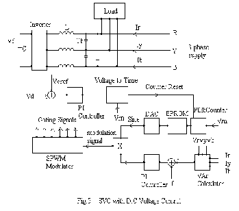
The VAr control loop here is essentially of first order due to link inductor and system losses. A high gain PI controller will accelerate the step response of this loop to a level where VAr commands are followed in less than a cycle. The slower voltage control loop will carry out the slow adjustment of phase angle needed to maintain the D.C. voltage constant. A combination of large valued capacitor, low valued inductor, fast VAr control loop and slow D.C. voltage control loop will ensure rapid VAr control with much reduced current amplitude oscillations in the link inductor. This scheme can very effectively provide reactive support during the power system transient conditions and can compensate a highly fluctuating load like an arc furnace.
The speed of response of the STATCOM is decided by two time delays – the rise time of STATCOM when a step change is applied to its reactive power command input
and the rise time behavior of the reactive demand calculator when the actual reactive flow in the source line changes suddenly. Hence, the Reactive Power Calculator has to extract the reactive component of the source current rapidly.The reactive command was shown as a VAr flow till now. However, the reactive component of the line current is enough for control purposes. A simple method to extract the reactive content in the current is explained here. Let the source current in one phase be i(t)
= I 0 +I 1 Sin (w t+q 1 ) +I 5 Sin (5w t+q 5 ) + I 7 Sin (7w t+q 7 )+.......
This covers the possibility of a non-linear load which draws harmonic currents and D.C. offsets too. Form the product of this current with unit amplitude cosine wave which is at 90 degrees in phase with that phase voltage. This product signal is called p(t).
P(t) = I 0 Cosw t+I 1 Cosw t Sin (w t+q 1 ) +I 5 Cosw t Sin (5w t+q 5 ) + I 7 Cosw t Sin (7w t+q 7 )+......
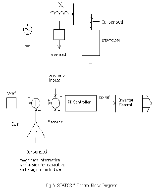
The integral of this product over integral number of fundamental periods will have content only from (I 1 Sinq 1 )/2 since all other products have zero average over fundamental period.Thus, the strategy is to form this product,integrate it for one period,sample the integrator output and hold the sample,reset the integrator after sampling and allow it integrate the product for the next period.The sampled integrator output will be a quantity proportional to the reactive component of the current.This output can be used as the reactive power signal in the STATCOM control block.The sampling and integrator reset are performed at zero crossing of sine wave and the product current is taken with the cosine wave.The cosine wave has to be pure,without harmonics. The control system block diagram is given in Figure 6. The terminal voltage is sensed and a PLL system is locked on to it. This is needed for controlling the inverter.The amplitude information is extracted from the sensed voltage and it is compared with the set reference value. The error decided the magnitude and polarity of the reactive current to be drawn by the STATCOM inverter from the ac system.A PI controller is used to speed up the response and reduce steady state error.The inner current loop on the sensed reactive current magnitude is used to pull down (in the case of capacitive compensation) the voltage reference value thereby effecting a droop characteristiv in the voltage regulation. ‘X’ represents the system impedance at the point of connection.Auxiliary inputs refer to the additional inputs into the control loop to make the STATCOM contribute to improvement of transient and dynamic stability. The loop gain of the control system is a strong function of system impedance X. Increasing the droop gain value reduces loop gain and increasing system impedance at the point of connection increases the loop gain.Hence the maximum system imedance condition must be identified and control system compensation must be done for that condition [1,4].
IJSER © 2014 http://www.ijser.org
International Journal of Scientific & Engineering Research, Volume 5, Issue 5, May-2014 1431
ISSN 2229-5518
The entire Proposed System will be tested using PSCAD/SIMULINK and the simulation results demonstrate the attractive performance characteristics of the proposed Design and Simulation of DSTATCOM for Power Quality Enhancement in Distribution Networks under various Fault Condition[4,9].
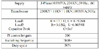
Simulation analysis is performed on 230/11kv three phase systems in PSCAD version 4.2 to study the performance of D-STATCOM and PWM Switched autotransformer. The system data as follows. DSTATCOM can use with different types of controllers and also we are designed and simulated of Distribution STATIC Compensator(DSTATCOM) with PI Controller to improve the quality of power under different abnormal conditions like single line to ground fault(SLG), double line to ground(DPG)fault in distribution networks with static non- linear loads.
TABLE I: System Parameters Used For Simulation
IJSER © 2014 http://www.ijser.org
International Journal of Scientific & Engineering Research, Volume 5, Issue 5, May-2014 1432
ISSN 2229-5518
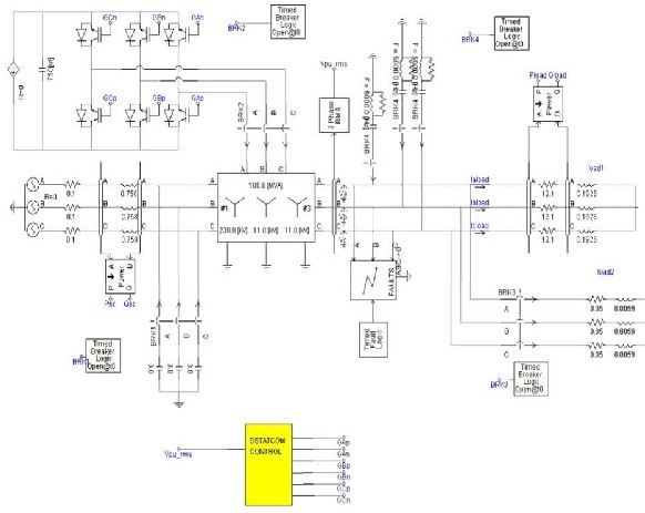
Fig. 7: test system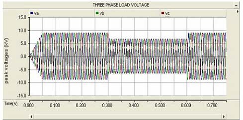
Fig. 8. Simulation results for load voltage during voltage sag without D-STATCOM
IJSER © 2014 http://www.ijser.org
International Journal of Scientific & Engineering Research, Volume 5, Issue 5, May-2014 1433
ISSN 2229-5518
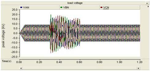
Fig.9.Simulation results for load voltage during voltage swell Without D-STATCOM.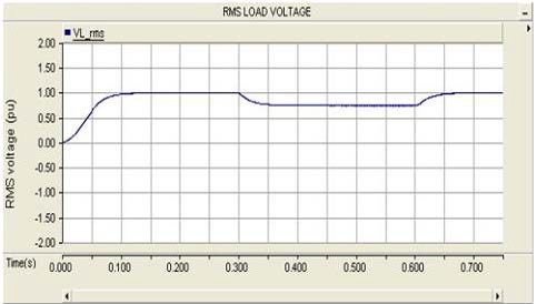
Fig.10.Simulation results for load voltage during voltage sag with D-STATCOM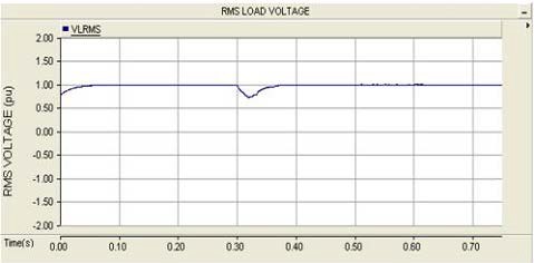
Fig. 11. Simulation result of load voltage during voltage sag with compensator
A New Voltage sag mitigation topology called PWM
switched autotransformer is modeled and simulated with
RMS voltage as a reference. This topology requires only
IJSER © 2014 http://www.ijser.org
International Journal of Scientific & Engineering Research, Volume 5, Issue 5, May-2014 1434
ISSN 2229-5518
one PWM switch per phase as compared to DSTATCOM
requires two switches per phase. The PWM
switched autotransformer does not require energy storage device for mitigation of voltage sag as compared to DSTATCOM requires energy storage elements. The voltage mitigation capability of D-STATCOM depends on energy storage device. Hence it is shows that PWM switched autotransformer is more economical than D- statacom. The PWM switched autotransformer and D- STATCOM for mitigation of voltage sag/swell could identify the
disturbance and capable of mitigating the disturbance by
maintaining the load voltage at desired magnitude and
THD within limits.
[1] Electric Power Research Institute (EPRI), “Power quality in commercial buildings,” Tech. Rep. BR-105018.
[2] M. F. Mc Granaghan, D. R. Muller and M. J. Samotyj, “Voltage sags in industrial systems,” IEEE Trans. Ind. Appl., vol. 29, no. 2, pp. 397–403,Mar./Apr. 1993.
[3] M. H. J. Bollen, Understanding Power Quality Problems: Voltage Sags and Interruptions. New York: IEEE Press, 2000. [4] Gareth A. Taylor, “Power quality hardware solutions for distribution systems: Custom power”, IEE North Eastern Centre Power Section Symposium, Durham, UK, 1995, pp.
11/1-11/9.
[5] Hendri Masid, Norman Moriun, Senan Mahmud, Azah
Mohamed and Sallehuddin Yusuf, “Design of a prototype D- Statcom for Voltage Sag Mitigation,” in Proc. 2004 National Power and Energy. Conf.,Kuallampur, Malaysia, Nov. 2004, pp. 61-66.
[6] Mahdi Mozaffari Legha and et al, ’’A new hybrid particle
swarm optimization approach for sizing and placement enhancement of distributed generation’’ IEEE Conference,
2155-5516; Pages 1277 - 1281.
[7] M. Mozaffari Legha, (2011) Determination of exhaustion
and junction of in distribution network and its loss maximum, due to geographical condition, MS.c Thesis. Islamic Azad University, Saveh Branch, Markazi Province, Iran
[8] J. R. Rostron and D.-M, Lee, “Voltage Sag and Over
Voltage Compensation Device with Pulse Width Modulating Switch Connected in Series With Autotransformer,” U.S. Patent
6 750 563, Jun. 2004.
[9] A. Hernandez, K. E. Chong, G. Gallegos, and E. Acha
“The implementation of a solid state voltage source in
PSCAD/EMTDC,” IEEE Power Eng. Rev., pp. 61-62, Dec
1998.
[10] L. Xu, Anaya-Lara, V. G. Agelidis, and E. Acha “Development of custom power devices for power quality enhancement,” in Proc. 9th ICHQP 2000, Orlando, FL, Oct.
2000, pp. 775-783.
[11] Y. Chen and B. T. Ooi, “STATCOM based on
multimodules of multilevel converters under multiple regulation feedback control,” IEEE Trans. Power Electron., vol. 14, pp.959-965, Sept. 1999.
[12] Dong-Myung Lee, Thomas G. Habetler, Ronald G. Harley, Thomas L.Keister and Joseph R. Rostran, “A Voltage sag Supporter Utilizing a PWM-Switched Autotransformer,” IEEE Trans. Power Electronics,Vol. 22, No. 2, Mar. 2007, pp.
626-635.
IJSER © 2014 http://www.ijser.org