Inte rnatio nal Jo urnal o f Sc ie ntific & Eng inee ring Re se arc h, Vo lume 3, Issue 2, February -2012 1
ISS N 2229-5518
“Signal Generator with Graphical User Interface
Control using Wireless Sensor Technology”
Keshavamurthy1, Dr.Dharmis htan K Varughese2, Dr. N.J.R Muniraj3
1Faculty, Atria Ins titute of Technology, Bangalore, INDIA-560024, Email: kes havamurthy_s@yahoo.com,Ph: +91- 9844662014
2 Profess ors , Department of EC, Karpagam College of Engineering, Coimbatore, INDIA.
3 Principal, Tejaa Shakthi Institute of Technology for Women, Coimbatore, INDIA.
Abstract — In the f ields of communications, signal processing, and in Electrical Engineering more generally, a signal is any time-varying or spatial-varying quantity. In the physical w orld, any quantity measurable through time or over space can be taken as a signal. Within a comp lex society, any set of human information or machine data can also be taken as a signal. Signal processing is an area of Electrical Engineering and
applied Mathe matics that deals w ith operations on or analysis of signals, in either discrete or continuous time to perf orm us ef ul operations on those signals. Signals of interest can include sound, images, time-varying measurement values and sensor data, f or example biological data such as Electrocardiograms, control system signals, telecommunication transmission signals such as radio signals, and many others. Si gnals are analog or digital e lectrical representations of time-varying or spatial-varying physical quantities. So w e can also realize how important is signal processing .It can not only convert data from one f orm (analog) to another (digital) and f acilitate its communication and other needs but as w ell vary parameters provided to practical circuits and appliances So w ith the context to signals w e do face certain problems that w e aim to solve:(1). We do f ind w ays to share data w ith other related hardw are and at a distance w ith modern transmission protocols such as I2C and SPI. (2). Conversion of data f rom analog to digital and vice versa. (3). Varying pow er or voltage signal applied to an appliance so that w e can save pow er consumption. (4). The development of a unit that can intelligently read the PC’s request at one end and vary the data and signals as and w hen required.
Key word— Dock light, Zigbee, Nanow att, I2C Mode, Encrypting, Watchdog and Graphical User Interface.
In nor mal embedded development w e use input/output signals thr ough I/O Ports, AD Converters, PW M signals and communication protocols I2C, RS232 and SPI. Lot of time is spent on gener ating above signals / debugging SW modules which deal with the above signals. The embedded signal gener ator with GUI generates signals fr om a microcontr oller .
This family of devices offers the advantages of all PIC18 microcontr ollers – namely, high computational per formance at an economical price w ith the addition of high-endurance, Enhanced Flash pr ogram memor y. In addition to these featur es, the PIC18F2455/2550/4455/4550 family intr oduces design enhancements that make these micr ocontr ollers a logical choice for many high-per formances, power sensitive applications.
This family of micr ocontr oller s is built with the
Nanowatt Technology and hence all of the devices in
the PIC18F2455/2550/4455/4 550 family incor porate a range of featur es that can significantly r educe pow er consumption dur ing oper ation.
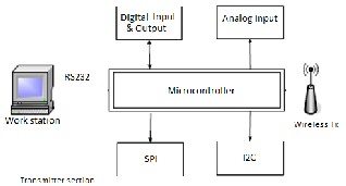
Figur e1.1. Tr ansmitter block diagr am
Figur e1.2. Receiver block diagr am
IJSER © 2012 http :// www.ijser.org
Inte rnatio nal Jo urnal o f Sc ie ntific & Eng inee ring Re se arc h, Vo lume 3, Issue 2, February -2012 2
ISS N 2229-5518
• Alternate Run Modes: By clocking the contr oller fr om the Timer1 source or the internal oscillator block, pow er consumption during code execution can be r educed by as much as 90%. Multiple Idle Modes: The contr oller can also r un with its CPU cor e disabled but the peripher als still active. In these states, pow er consumption can be r educed even further , to as little as
4%, of normal operation r equir ements.
• On-the-Fly Mode Switching: The pow er-managed modes ar e invoked by user code during oper ation, allowing the user to incorpor ate power-saving ideas into their applications softwar e design.
• Low Consumption in Key Modules: The pow er
r equir ements for both Timer1 and the Watchdog Timer ar e minimized.
Devices in the PIC18F2455/2550/4455/4550 family incorporate a fully featur ed Univer sal Serial Bus Communications module that is compliant with the USB Specification Revision 2.0. The module suppor ts both low-speed and full-speed communication for all
supported data tr ansfer types. It also incor porates its ow n on-chip tr ansceiver and 3.3V r egulator and supports the use of external tr ansceiver s and voltage r egulators. All of the devices in the PIC18F2455/2550/4455/4550 family offer tw elve differ ent oscillator options, allowing user s a w ide range of choices in developing application har dwar e. Besides its availability as a clock sour ce, the inter nal oscillator block pr ovides a stable r efer ence sour ce that gives the family additional featur es for r obust oper ation:
• Fail-Safe Clock Monitor: This option constantly monitor s the main clock sour ce against a r efer ence signal pr ovided by the inter nal oscillator . If a clock failur e occurs, the controller is switched to the internal oscillator block, allowing for continued low-speed operation or a safe application shutdown.
• Two -Speed Start-up: This option allows the internal
oscillator to serve as the clock sour ce fr om Power -on Reset, or wake-up fr om Sleep mode, until the primary clock sour ce is available.
Port A: PORT-A is an 8-bit w ide, bidir ectional port. The corr esponding data dir ection r egister is TRISA. Setting a TRISA bit (= 1) w ill make the corr esponding PORTA pin an input (i.e., put the corr esponding output driver in a high-impedance mode). Clear ing a TRISA bit (= 0) w ill make the corr esponding PORTA pin an output (i.e., put the contents of the output latch on the selected pin).
Reading the PORTA r egister r eads the status of the
pins, wher eas writing to it, w ill write to the port latch. The Data Latch (LATA) r egister is also memory
mapped. Read-modify-wr ite operations on the LATA r egister r ead and write the latched output value for PORTA.
The other PORTA pins ar e multiplexed with analog inputs, the analog VREF+ and VREF- inputs and the comparator voltage r efer ence output. The operation of pins RA3:RA0 and RA5 as A/D converter i nputs is selected by clear ing or setting the contr ol bits in the
ADCON1 r egister (A/D Contr ol Register 1). Pins RA0 through RA5 may also be used as comparator inputs or outputs by setting the appr opr iate bits in the CMCON r egister .
Port B: PORTB is an 8-b it wide, bidir ectional port. The corr esponding data dir ection r egister is TRISB. Setting a TRISB bit (= 1) will make the corr esponding PORTB pin an input (i.e., put the corr esponding output driver in a high-impedance mode). Clearing a TRISB bit (= 0) w ill make the corr esponding PORTB pin an output (i.e., put the contents of the output latch on the selected pin). The Data Latch r egister (LATB) is also memory mapped. Read-modify-write operations on the LATB r egister r ead and write the latched output value for PORTB.
Each of the PORTB pins has a w eak internal pull -up.
A single contr ol bit can turn on all the pull-ups. This is
per formed by clearing bit, RBPU (INTCON2<7>). The w eak pull-up is automatically tur ned off when the port pin is configur ed as an output. The pull-ups ar e disabled on a Pow er-on Reset.
Port C: PORTC is an 8-bit w ide, bidir ectional port. The
corr esponding data dir ection r egister is TRISC. Setting a
TRISC bit (= 1) will make the corr esponding PORTC pin an input (i.e., put the corr espon ding output driver in a high-impedance mode). Clear ing a TRISC bit (= 0) w ill make the corr esponding PORTC pin an output (i.e., put the contents of the output latch on the selected pin).
The Data Latch r egister (LATC) is also memory mapped. Read-modify-write operations on the LATC
r egister r ead and write the latched output value for PORTC. PORTC is multiplexed with several per ipheral functions. The pins have Schmitt Tr igger input buffer s. RC1 is normally configur ed by configuration bit,
CCP2MX, as the default peripher al pin of the CCP2 module.
Port D: PORTD is an 8-bit w ide, bidir ectional port. The corr esponding data dir ection r egister is TRISD. Setting a TRISD bit (= 1) w ill make the corr esponding PORTD pin an input (i.e., put the corr esponding output driver in a high-impedance mode). Clear ing a TRISD bit (= 0) w ill make the corr esponding PORTD pin an output (i.e., put the contents of the output latch on the selected pin). The Data Latch r egister (LATD) is also memory mapped.
IJSER © 2012 http :// www.ijser.org
Inte rnatio nal Jo urnal o f Sc ie ntific & Eng inee ring Re se arc h, Vo lume 3, Issue 2, February -2012 3
ISS N 2229-5518
Read-modify-write operations on the LATD r egister r ead and write the latched output value for PORTD. All pins on PORTD ar e implemented w ith Schmitt Tr igger input buffers.
Each pin is individually configurable as an input or
output. Thr ee of the PORTD pins ar e multiplexed with outputs P1B, P1C and P1D of the Enhanced CCP module.
Port E: For 40/44-pin devices, PORTE is a 4-bit wide port. Thr ee pins (RE0/RD/AN5, RE1/W R/AN6 and RE2/CS/ AN7) ar e individually configurable as inputs or outputs. These pins have Schmitt Trigger input buffer s. When selected as an analog input, these pins w ill r ead as ‘0’s. The corr esponding data dir ection r egister is TRISE. Setting a TRISE bit (= 1) w ill make the corr esponding PORTE pin an input (i.e., put the corr esponding output dr iver in a high-impedance mode). Clearing a TRISE bit (= 0) w ill make the corr esponding PORTE pin an output (i.e., put the contents of the output latch on the selected pin). TRISE contr ols the dir ection of the RE pins, even when they ar e being used as analog inputs. The user must make sur e to keep the pins configur ed as inputs when using them as analog inputs. The upper four bits of the TRISE r egister also contr ol the oper ation of the Parallel Slave Port.
The Master Synchr onous Ser ial Port (MSSP) module is a
ser ial inter face, useful for communicating w ith other peripher al or micr ocontr oller devices. These peripheral devices may be serial EEPROMs, shift r egisters,display drivers, A/D conver ters, etc.
The MSSP module has thr ee associated contr ol r egister s.These include a status r egister (SSPSTAT) and tw o contr ol r egister s (SSPCON1 and SSPCON2). The use of these r egisters and their individual Configur ation bits differ significantly depending on whether the MSSP module is oper ated in SPI or I2C mode.
The MSSP module has four r egisters for SPI mode operation. These ar e:
• MSSP Contr ol Register 1 (SSPCON1)
• MSSP Status Register (SSPSTAT)
• Ser ial Receive/Tr ansmit Buffer Register
(SSPBUF)
• MSSP Shift Register (SSPSR) – Not dir ectly accessible
SSPCON1 and SSPSTAT ar e the contr ol and status r egister s in SPI mode oper ation. The SSPCON1 r egister is
r eadable and writable. The low er six bits of the SSPSTAT
ar e r ead-only.
The upper two bits of the SSPSTAT ar e r ead/ write. SSPSR is the shift r egister used for shifting data in or out. SSPBUF is the buffer r egister to which data bytes ar e written to or r ead fr om .In r eceive operations, SSPSR and SSPBUF together cr eate a double-buffer ed r eceiver . When SSPSR r eceives a complete byte, it is transferr ed to SSPBUF and the SSPIF interr upt is set .Dur ing transmission, the SSPBUF is not double buffer ed .A write to SSPBUF will write to both SSPBUF and SSPS
The master contr oller (Pr ocessor 1) initiates the data transfer by sending the SCK signal .Data is shifted out of both shift r egisters on their pr ogr ammed clock edge and latched on the opposite edge of the clock.
Both pr ocessors should be pr ogrammed to the same Clock Polar ity (CKP), then both contr ollers w ould send and r eceive data at the same time. Whether the data is meaningful (or dummy data) depends on the application softwar e. This leads to thr ee scenar ios for data transmission:
• Master sends data – Slave sends dummy data
• Master sends data – Slave sends data.
• Master sends dummy data – Slave sends data.
In Master mode, the data is tr ansmitted /r eceived as soon as the SSPBUF r egister is wr itten to. If the SPI is only going to r eceive, the SDO output could be disabled (pr ogrammed as an input). The SSPSR r egister will continue to shift in the signal pr esent on the SDI pin at the pr ogrammed clock r ate. As each byte is r eceived , it will be loaded into the SSPBUF r egister as if a normal r eceived byte (interr upts and status bits appropr iately set). This could b e useful in r eceiver applications as a ‚Line Activity Monitor ‛ mode.
In Slave mode, the data is transmitted and r eceived
as the exter nal clock pulses appear on SCK. When the last bit is latched, the SSPIF interrupt flag bit is set. W hile in Slave mode, the external clock is supplied by the exter nal
clock sour ce on the SCK pin.
This exter nal clock must meet the minimum high and low times as specified in the electr ical specifications
.While in sleep mode, the slave can transmit/r eceive
data. When a byte is r eceived, the device can be configur ed to wake- up fr om Sleep.
IJSER © 2012 http :// www.ijser.org
Inte rnatio nal Jo urnal o f Sc ie ntific & Eng inee ring Re se arc h, Vo lume 3, Issue 2, February -2012 4
ISS N 2229-5518
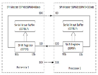
Figur e3.1. SPI connection
The MSSP module in I2C mode fully implements all master and slave functions (including general call support) and pr ovides interrupts on Start and Stop bits in hardwar e to determine a fr ee bus (multi-master function). The MSSP module implements the standar d mode specifications, as w ell as 7-bit and 10-bit addr essing .Two pins ar e used for data transfer :
• Ser ial clock (SCL) – RB1/AN10/INT1/SCK/SCL
• Ser ial data (SDA) – RB0/AN12/INT0/FLT0/SDI/SDA
The user must configur e these pins as inputs by setting the associated TRIS bits.
Each Captur e/Compar e/PW M module is associated w ith a contr ol r egister (gener ically, CCP x CON) and a data r egister (CCP Rx). The data r egister , in tur n, is comprised of two 8-bit r egister s: CCP Rx L (low byte) and CCP Rx H (high byte). All r egister s ar e both r eadable and wr itable.
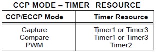
The CCP modules utilize Timers 1, 2 or 3, depending
on the mode selected. Timer1 and Timer3 ar e available to modules in Captur e or Compar e modes, while Timer2 is available for modules in PW M mode.
In Captur e mode, the CCPR x H : CCPR x L r egister pair captur es the 16-bit value of the TMR1 or TMR3 r egisters when an event occur s on the corr esponding CCP x pin.
The event is selected by the mode select
bits,CCPxM3:CCPxM0 (CCP x CON<3:0>). When a
captur e is made, the interr upt r equest flag bit, CCP x IF, is set; it must be clear ed in softwar e. If another captur e occurs befor e the value in r egister CCPRx is r ead, the old captur ed value is overwritten by the new captur ed value.
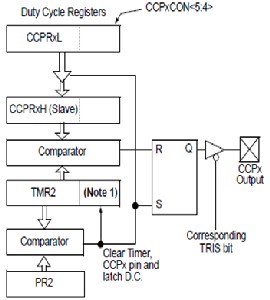
Figur e3.2. PWM generator block diagram.
3.3.1. PWM Outp ut
Figur e3.2. PW M gener ation blockdiagr am and PWM
output.
In Pulse-W idth Modulation (PWM) mode:
IJSER © 2012 http :// www.ijser.org
Inte rnatio nal Jo urnal o f Sc ie ntific & Eng inee ring Re se arc h, Vo lume 3, Issue 2, February -2012 5
ISS N 2229-5518
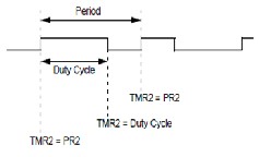
The CCPx pin pr oduces up to a 10-bit r esolution PW M output. A PW M output has a time base (per iod) and a time that the output stays high (duty cycle).The fr equency of the PW M is the inverse of the per iod (1/per iod).
3.3.1. PWM period and du ty cycle
The PWM per iod is specified by writing to the PR2 r egister w hich is given by![]()
PW M fr equency is defined as 1/[PW M period].
When TMR2 is equal to PR2, the following thr ee events occur on the next incr ement cycle:
TMR2 is clear ed
• The CCPx pin is set (exception: if PW M duty cycle =
0%, the CCPx pin w ill not be set)
• The PW M duty cycle is latched fr om CCPRxL into
CCPRxH.
The PW M duty cycle is specified by wr iting to the
CCPRxL r egister and to the CCPxCON<5:4> bits. Up to 10-bit r esolution is available.
The CCPRxL contains the eight MSBs and the
CCPxCON<5:4> bits contain the tw o LSBs.
CCPRxL and CCPxCON<5:4> can be wr itten to at anytime.But the duty cycle value is not latched intoCCPRxH until after a match betw een PR2 and TMR2 occurs (i.e., the per iod is complete).
In PW M mode, CCPRxH is a r ead-only r egister .
If the PW M duty cycle value is longer than the PWM
period, the CCPx pin w ill not be clear ed.
The CCPRxH r egister and a 2 -bit inter nal latch ar e used to double-buffer the PWM duty cycle. This double- buffer ing is essential for glitch less PW M operation.
W hen the CCPRxH and 2-bit latch match TMR2, concatenated with an internal 2-bit Q clock or 2 bits of the TMR2 pr esale, the CCPx pin is clear ed. The maximum PW M r esolution (bits) for a given PW M fr equency is given by the equation:![]()
The XBee/XBee-PRO ZB RF Modules ar e designed to operate within the ZigBee pr otocol and support the unique needs of low-cost, low-power w ir eless sensor networ ks. The modules r equir e minimal pow er and pr ovide r eliable delivery of data betw een r emote devices.
The modules operate w ithin the ISM 2.4 GHz fr equency
band and ar e compatib le with the following: •XBee RS -
232 Adapter •XBee RS-485 Adapter •XBee Analog I/O
Adapter •XBee Digital I/O Adapter •XBee Sensor •XBee USB Adapter •XStick •Connect Port X Gat eways •XBee Wall Router .
Metal obj ects next to the antenna or betw een
transmitting and r eceiving antennas can often block or
r educe the transmission distance. Some obj ects that ar e often over looked ar e metal poles, metal studs or beams in structur es, concr ete (it is usually r einforced with metal r ods), metal enclosur es, vehicles, elevators, ventilation ducts.
The XBee RF Modules inter face to a host device thr ough a logic-level asynchr onous ser ial port. Thr ough its ser ial port, the module can communicate w ith any logic and voltage compatible UART; or thr ough a level translator to any ser ial device (for example: thr ough a RS-232 or USB inter face board). The XBee modules maintain small buffer s to collect r eceived ser ia l and RF data. The ser ial r eceive buffer collects incoming serial char acter s and holds them until they can be pr ocessed. The ser ial transmit buffer collects data that is r eceived via the RF link that will be tr ansmitted out the UART
When ser ial data enter s the RF module thr ough the DIN Pin (pin 3), the data is stor ed in the serial r eceive buffer until it can be pr ocessed. Under certain conditions, the module may not be able to pr ocess data in the ser ial r eceive buffer immediately. If lar ge amounts of ser ial data ar e sent to the module, CTS flow contr ol may be r equir ed to avoid over flowing the ser ial r eceive buffer .
Cases in which the serial receive buffer may become
full and possibly overflow:
1. If the module is r eceiving a cont inuous str eam of RF data, the data in the ser ial r eceive buffer will not be transmitted until the module is no longer r eceiving RF data.
2. If the module is transmitting an RF data packet, the
module may need to discover the destination addr ess or establish a r oute to the destination. After transmitting the data, the module may need to r etr ansmit the data if an acknow ledgment is not r eceived, or if the transmission is a br oad-cast. These issues could delay the pr ocessing of data in the ser ial r eceive buffer.
When RF data is r eceived, the data is moved into the ser ial tr ansmit buffer and sent out the UART. If the ser ial
IJSER © 2012 http :// www.ijser.org
Inte rnatio nal Jo urnal o f Sc ie ntific & Eng inee ring Re se arc h, Vo lume 3, Issue 2, February -2012 6
ISS N 2229-5518
transmit buffer becomes full enough such that all data in a r eceived RF packet w on’t fit in the serial transmit buffer , the entir e RF data packet is dr opped.
Cases in which the serial transmit buffer may become full resulting in dropped RF packets
1. If the RF data r ate is set higher than the inter face data rate of the module, the module could r eceive data faster than it can send the data to the host.
2. If the host does not allow the module to transmit data out fr om the ser ial transmit buffer because of being held off by har dwar e flow contr ol.
If CTS flow contr ol is enabled (D7 command), when the ser ial r eceive buffer is 17 bytes away fr om being full, the module de-asserts CTS (sets it high) to signal to the host device to stop sending serial data. CTS is r e-asserted after the ser ial r eceive buffer has 34 bytes of space.
When not r eceiving or transmitting data, the RF module is in Idle Mode. The module shifts into the other modes of operation under the following conditions: •Tr ansmit Mode (Ser ial data in the ser ial r eceive buffer is r eady to be packetized) •Receive Mode (Valid RF data is r eceived through the antenna) •Sleep Mode (End Devices only)
•Command Mode (Command Mode Sequence is issued
When ser ial data is r eceived and is r eady for packetization, the RF module will exit Idle Mode and attempt to transmit the data. The destination addr ess determines which node(s) w ill r eceive the data. Prior to transmitting the data, the module ensur es that a 16-bit networ k addr ess and r oute to the destination node have been established. If the destination 16 -bit netw or k addr ess is not known, netw or k addr ess discovery w ill take place.
If a r oute is not known, r oute discovery will take
place for the pur pose of establishing a r oute to the
destination node. If a module w ith a matching netw ork addr ess is not discover ed, the packet is discarded. The data will be tr ansmitted once a r oute is established. If r oute discovery fails to establish a r oute, the packet will be discar ded.
4.5. Zig Bee Security Model
ZigBee secur ity is applied to the Networ k and APS layers. Packets ar e encrypted with 128-bit AES encryption. A networ k key and optional link key can be used to encrypt data. Only devices with the same keys ar e able to communicate together in a netw or k. Router s and end
devices that will communicate on a secur e netw or k must obtain the corr ect security keys.
ZigBee end devices ar e intended to be battery -pow er ed
devices capable of sleeping for extended per iods of time. Since end devices may not be awake to r eceive RF data at a given time, r outer s and coordinators ar e equipped with additional capabilities (including packet buffering and extended transmission timeouts) to ensur e r eliable data
delivery to end devices. ZigBee defines a tr ust center device that is r esponsible for authenticating devices that j oin the netw or k. The trust center also manages link key distr ibution in the netw or k.
If APS security is enabled, the APS header and data payload ar e authenticated w ith 128-bit AES. A hash is per formed on these fields and appended as a 4-byte message integrity code (MIC) to the end of the packet. This MIC is differ ent than the MIC appended by the networ k layer . The MIC allows the destination device to ensur e the message has not been changed. If the destination device r eceives a packet and the MIC does not match the destination device’s own hash of the data, the packet is dr opped.
The netw or k key is used to encrypt the APS layer and application data. In addition to encrypting application messages, networ k secur ity is also applied to r oute r equest and r eply messages, APS commands, and ZDO commands. Netw or k encry ption is not applied to MAC layer tr ansmissions such as beacon tr ansmissions, etc. If security is enabled in a networ k, all data packets w ill be encrypted w ith the networ k key. Packets ar e encrypted and authenticated using 128-bit AES. This is shown in the figur e below.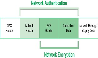
Figure 4: Network security layer
IJSER © 2012 http :// www.ijser.org
Inte rnatio nal Jo urnal o f Sc ie ntific & Eng inee ring Re se arc h, Vo lume 3, Issue 2, February -2012 7
ISS N 2229-5518
C# is an obj ect-or iented pr ogramming language developed by Micr osoft Cor poration. C# sour ce code as w ell as those of other .NET languages is compiled into an intermediate byte code called Micr osoft Inter mediate Language. C# is pr imar ily der ived fr om the C, C++, and Java pr ogramming languages w ith some featur es of Micr osoft's Visual Basic in the mix. C# is used to develop applications for the Micr osoft .NET envir onment. .NET offer s an alter native to Java development. Micr osoft's Visual Studio .NET development envir onment incorporates several differ ent languages including ASP.NET, C#, C++, and J# (Micr osoft Java for .NET), all of which compile to the Common Language Runtime.
The C# code that we write is supported on Micr osoft Visual studio 2008 and we handle all our operations by this code. Thr ough this code w e not only open the ser ial port and per form input and output oper ations but also r eceive analog values and cause their conver sion to digital values and display them as w ell as tr ansmit them to the micr ocontr oller .
What is most important is that thr ough this code w e ar e able to var y the fr equency and duty cycle of our PWM signal and also send the micr ocontr oller the changes so that it can communicate with the r emote terminal wher e the pow er of the appliance can be var ied.
MPLAB X IDE is a softwar e program that r uns on a PC (W indows®, Mac OS®, Linux®) to develop applications for Micr ochip microcontrollers and digital signal contr ollers. It is called an Integr ated Development Envir onment, or IDE, because it pr ovides a single integr ated
‚envir onment‛ to develop code for emb edded
microcontr ollers.
The per ipherals and the amount of memory an application needs to r un a pr ogr am lar gely determines which PICmicr o MCU to use. Other factors might include the power consumed by the micr ocontr oller and its ‚form factor ,‛ i.e., the size and char acter istics of the physical package that must r eside on the tar get design.
A development system for embedded contr ollers is a
system of pr ograms r unning on a desktop PC to help write, edit, debug and progr am code – the intelligence of embedded systems applications – into a micr ocontr oller . MPLAB IDE, r uns on a PC and contains all the components needed to design and deploy embedded systems applications.
Once the code builds with no err or s, it needs to be tested.
MPLAB IDE has components called ‚deb uggers‛ and fr ee
softwar e simulators for all PICmicr o and dsPIC devices to help test the code. Even if the hardwar e is not yet finished, you can begin testing the code with the simulator , a softwar e pr ogram that simulates the execution of the microcontr oller . The simulator can accept a simulated input (stimulus), in order to model how the firmwar e r esponds to exter nal signals. The simulator can measur e code execution time, single-step through code to watch variables and peripher als, and trace the code to generate a detailed r ecor d of how the pr ogram r an.
Once the hardwar e is in a pr ototype stage, a
hardwar e debugger , such as MPLAB ICE or MPLAB ICD
2 can be used. These debugger s r un the code in r eal time
on your actual application. The MPLAB ICE physically r eplaces the micr ocontr oller in the tar get using a high - speed pr obe to give you full contr ol over the har dwar e in your design.
The MPLAB ICD 2 uses special cir cuitr y built into many Micr ochip MCUs w ith Flash pr ogr am memory and can ‚see into‛ the tar get micr ocontr ollers pr ogram and
data memory. The MPLAB ICD 2 can stop and start pr ogram execution, allowing you to test the code w ith the microcontr oller in place on the application.
Microsoft Visual Studio is an integrated development envir onment (IDE) fr om Micr osoft. It can be used to develop console and graphical user inter face applications along with Windows Forms applications, w eb sites, web applications, and w eb services in both native code together w ith managed code for all platforms supported by Micr osoft Windows, W indows Mobile, W indows CE,
.NET Fr amew or k, .NET Compact Framew or k and
Micr osoft Silver light.
Visual Studio includes a code editor supporting IntelliSense as w ell as code r efactoring. The integr ated debugger w or ks both as a sour ce-level debugger and a machine-level debugger .
It accepts plug-ins that enhance the functionality at
almost every level—including adding support for source- contr ol systems (like Subver sion and Visual Sour ceSafe) and adding new toolsets like editors and visual designers for domain-specific languages or toolsets for other aspects of the softwar e development lifecycle.
Visual Studio, like any other IDE, includes a code editor that supports syntax high lighting and code completion using IntelliSense for not only var iables, functions and methods but also language constructs like loops and quer ies.
IJSER © 2012 http :// www.ijser.org
Inte rnatio nal Jo urnal o f Sc ie ntific & Eng inee ring Re se arc h, Vo lume 3, Issue 2, February -2012 8
ISS N 2229-5518
IntelliSense is supported for the included languages, as w ell as for XML and for Cascading Style Sheets and JavaScr ipt when developing w eb sites and web applications. Auto complete suggestions ar e popped up in a modeless list box, over laid on top of the code editor . In Visual Studio 2008 onwar ds, it can be made temporar ily semi-transpar ent to see the code obstr ucted by it. The code editor is used for all supported languages.
Visual Studio includes a debugger that wor ks both as a sour ce-level debugger and as a machine-level debugger . It wor ks w ith both managed code as w ell as native code and can be used for debugging applications wr itten in any language suppor ted by Visual Studio. In addition, it can also attach to r unning pr ocesses and monitor and debug those pr ocesses. If sour ce code for the r unning pr ocess is available, it displays the code as it is being r un. If sour ce code is not available, it can show the disassembly. The Visual Studio debugger can also cr eate memory dumps as well as load them later for debugging. Multi-thr eaded pr ogr ams ar e also suppor ted. The debugger can be configur ed to be launched when an application r unning outside the Visual Studio envir onment crashes.
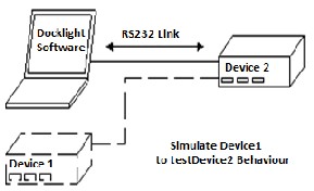
Docklight can send out user-defined sequences according to the pr otocol used and it can r eact to incoming sequences. This makes it possible to simulate the behavior of a ser ial communication device, which is particularly useful for gener ating test conditions that ar e har d to r epr oduce with the or iginal device (e.g. pr oblem conditions).
Figur e 5.1.Simulated device
In many test cases you will need to check for a specific sequence within the RS232 data that indicates a pr oblem condition. Dock light manages a list of such data sequences for you and is able to per for m user -defined actions after detecting a sequence, e.g. taking a snapshot of all
communication data befor e and after the err or message was r eceived.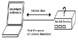
Figur e5.2. Test protocol
All ser ial communication data can be logged using two differ ent file formats: use plain text format for fast logging and storing huge amounts of data. Or cr eate a HTML file with styled text that lets you easily distinguish betw een incoming and outgoing data or additional infor mation .
1. W ith advancements in Zigbee pr otocol, the r ange which is a maj or operational barr ier can be incr eased.
2. Along with the Zigbee Coor dinator and Zigbee End Device, if w e connect a r outer then our setup can w or k for many r emote terminals.
3. They can be used in industr ial contr ol rooms in or der to handle the appliances by sending PWM signals fr om a distance and use this idea in a pr oductive manner .
4. It is r eally effective as a contr ol device when the end applications ar e to be contr olled from a distance i.e. in case of harsh envir onments. Ex: industrial heater s, lighting etc.
5. Wir eless measur ing of analog data for example as w e can connect a t emperatur e sensor cum logger , gas sensor etc.
6. W e can achieve a better r esolution by incr easing it up to
10 bit.
7. Since it has a better range as w e use Zigbee, our design
can per form switching application to appliances fr om a distance. Data can be r ead fr om and written to as w e need for Digital Processing.
The signal generated out of this module can be used in any 8/16/32 bit embedded system for rapid pr ototyping/ debugging. This unit has the capability to vary the parameters of the PWM by which w e can vary the signal pow er supplied to the end user s. Mor e flexibility in our approach as we can modify the execution code as and when needed to add new utilities. Less har dwar e and time involved in the generation of PW M than
IJSER © 2012 http :// www.ijser.org
Inte rnatio nal Jo urnal o f Sc ie ntific & Eng inee ring Re se arc h, Vo lume 3, Issue 2, February -2012 9
ISS N 2229-5518
conventional ways. Apar t fr om this the unit will also have the capability to monitor the digital I/O lines and analog values fr om the r emote ter minal.
Today w e have learned to upgr ade our daily life applications w ith new technologies. W e have made an effor t to pr ovide a design which can be used in a number of ways as per the r equir ement. It can pr ovide industr ial applications as w ell as being equally effective in a simple house hold. For example, w e can use our simple unit to contr ol a heater at home. It can set tw o thr esholds and by the help of our temperatur e sensor , w e can detect if the temperatur e has gone up to the upper thr eshold and by the help of the r elays in our design we can switch off the heater . So it comes so handy in a simple household.
Similar ly, we have contr ol application of our unit in industr ial heating and gas furnaces, lighting, motor s etc. Fr om a distant contr ol r oom, w e can vary the power of the appliances as well as monitor the temperatur e and gas levels etc and accor ding to our r eal time deadlines, can turn it off using the r elays or r educe pow er applied to it by using our PW M module.
Hence w e see how our embedded unit handles a lot of functionalities w ith simplified har dwar e and with a high accuracy rate. It also r educes manpow er and hazar dous r esults. So w e have achieved what we had aimed for and w e can r eally put it to use effectively.
*1+ T. Kikuc hi, T. Ke njo , and S. Fukuda, ‚Re mo te labo rato ry fo r a brushle ss dc mo to r,‛ IEEE Trans. Educ., vo l. 44, May 2001.
[2] A. Hatto ri, N. S uzuki, S. S uzuki, A. Takatsu, M. P. Baue r, A.
Hirne r, S.Takahashi, S. Kobay ashi, Y. Yamazaki, Y. Adac hi, T.
Kumano , and A.Ike mo to , ‚Te le -v irtual surg e ry with sharing tac tile se nsatio ns be twee n Japan and Ge rmany ,‛ in Proc. 22nd Annu. Int. Co nf. IEEE Eng inee ring Me dic ine Bio logy Soc., Chic ago , IL, July 23 –
28, 2000, pp. 2423 –2425.
[3] Pallo ff R. and Pratt K., The V irtual S tude nt - A Pro file and
Guide to Wo rking with Online Le arne rs , Jossey - Bass, 2003, ISBN
0-7879- 6474-3
*4+ I.A. Gro ut, J.Walsh, T. O’S he a and M. Canav an, A Loc al and
Re mo te Labo rato ry Use r Expe rime ntatio n Access Arrange me nt using Dig ital Prog rammable Log ic , Procee dings o f the Re mo te Eng inee ring and V irtual Instrume ntatio n Sy mposium (REV 2004), Se pte mbe r 2004, V illac h, Austria
[5] J. Murphy , I. Gro ut, J. Walsh, and T. O'S he a, Loc al and Re mo te
Labo rato ry Use r Expe rime ntatio n Access using Dig ital Prog rammable Log ic, Inte rnatio nal Jo urnal o f Online Eng ine e ring , vo l. 1, Oc to be r 2005, http://www.i-jo e.co m
[6] Ro hrig, C. and Joc hhe im, A., The V irtual Lab fo r contro lling re al
e xpe rime nts v ia Inte rne t, Procee dings o f the IEEE Inte rnatio nal
Sy mpo sium o n Co mpute r Aide d Co ntro l Sy ste m De sig n, 1999, pp
279-284
[7] Best R. E., Phase -locke d loo ps: theo ry , de sig n, and
applic atio ns, 1984,IS BN 0070050503
[8] Ro hde U.L., Dig ital PLL fre que ncy sy nthesize rs: theo ry and de sig n, Pre ntice -Hall, Lo ndo n, 1983, IS BN 0132142392
[9] Burbidge , M.J. and Ric hardso n, A.M., S imple dig ital te st
appro ac h fo r e mbe dde d c harge -pump phase -locke d loo ps,
Elec tro nic s Le tte rs, Vo lume 37, Issue 22, 25th Oc to be r 2001, pp 1318 -
1319
[10]. iee e xplo re.ieee .o rg (fo r info rmatio n o n sig nal g e ne rato rs)
[11]http://www.matrixmul time dia.c o m,www.sparkfun.co m/datash
e e ts/Wire le ss/Zig bee/XBee -2.5-Datashee t ( fo r Zig bee mo dule ) [12]www.so urceco deo nline.co m/list?q=e mbe dde d_sy ste m_pro jec ts
_o n_ieee _pape r
[13].www.ieee pape r.co m/free -ieee -pape rs-e mbe dde d-sy ste m-
31.htm
[14]http://www.alibaba.co m/RS232
IJSER © 2012 http :// www.ijser.org