International Journal of Scientific & Engineering Research Volume 3, Issue 1, January-2012 1
ISSN 2229-5518
Reconfigurable Embedded Multiprocessor
Architecture with ARISE interface using FPGA
M. Abragam Siyon Sing, K. Vidya
Abstract—Modern Embedded multiprocessor design presents challenges and opportunities that stem from task coarse granularity and the large number of inputs and outputs for each task. They are complex systems that often require years to design and verify. A significant factor is that engineers must allocate a disproportionate share of their effort to ensure that modern FPGA chips architecture behave correctly. Therefore, in order to reduce the complexity in design and verification, a new architecture is proposed which is implemented using FPGA. In this, the Embedded Processors are integrated with the shared memory system, synthesized that this system on an FPGA environment and ARISE interface is used to extent the processor and this interface is used once. Then, an arbitrary number of processors can be attached, via the interface, which can be a reconfigurable unit. Using this interface, more number of processor cores can be attached and bit to bit conversions can also be possible from one processor to another processor, that is, asymmetric processors can be built.
Index Terms – ARISE Interface, VLIW Processor, FPGA, Wrapper.
—————————— • ——————————
1 INTRODUCTION
Any system that incorporates two or more microprocessors working together to perform one or more related tasks is commonly referred to as a multiprocessor system. In a multiprocessing system, all CPUs may be equal, or some may be reserved for special purposes. A combination of hardware and operating-system software design considerations determines the symmetry in a given system. For example, hardware or software considerations may require that only one CPU respond to all hardware interrupts, whereas all other work in the system may be distributed equally among CPUs; or execution of kernel-mode code may be restricted to only one processor (either a specific processor, or only one processor at a time), whereas user-mode code may be executed in any combination of processors. Multiprocessing systems are often easier to design if such restrictions are imposed, but they tend to be less efficient than systems in which all CPUs are utilized.
Systems that treat all CPUs equally are called symmetric multiprocessing (SMP) systems. Because of the flexibility of SMP and because of its cost being relatively low, this architecture has become the standard for mainstream multiprocessing. Multitasking operating systems can run processes on any CPU in a SMP system because each processor has the same view of the machine.
In systems where all CPUs are not equal, system resources may be divided in a number of ways, including asymmetric multiprocessing (ASMP), non-uniform memory access (NUMA) multiprocessing, and clustered multiprocessing In multiprocessing, the processors can be used to execute a single sequence of instructions in multiple contexts (single- instruction, multiple-data or SIMD, often used in vector processing), multiple sequences of instructions in a single context (multiple-instruction, single-data or MISD, used for redundancy in fail-safe systems and sometimes applied to
describe pipelined processors or hyper-threading), or multiple sequences of instructions in multiple contexts (multiple-instruction, multiple-data or MIMD).
Tightly-coupled multiprocessor systems contain multiple CPUs that are connected at the bus level. These CPUs may have access to a central shared memory (SMP or UMA), or may participate in a memory hierarchy with both local and shared memory (NUMA). The IBM p690 Regatta is an example of a high end SMP system. Intel Xeon processors dominated the multiprocessor market for business PCs and were the only x86 option until the release of AMD's Opteron range of processors in 2004. Both ranges of processors had their own on board cache but provided access to shared memory; the Xeon processors via a common pipe and the Opteron processors via independent pathways to the system RAM.
Chip multiprocessors, also known as multi-core computing, involves more than one processor placed on a single chip and can be thought of the most extreme form of tightly-coupled multiprocessing. Mainframe systems with multiple processors are often tightly-coupled.
Loosely-coupled multiprocessor systems (often referred to as clusters) are based on multiple standalone single or dual processor commodity computers interconnected via a high speed communication system (Gigabit Ethernet is common). A Linux Beowulf cluster is an example of a loosely-coupled system.
Tightly-coupled systems perform better and are physically smaller than loosely-coupled systems, but have historically required greater initial investments and may depreciate rapidly; nodes in a loosely-coupled system are usually inexpensive commodity computers and can be recycled as independent machines upon retirement from the cluster. Power consumption is also a consideration. Tightly-coupled systems tend to be much more energy efficient than clusters.
IJSER © 2012 http://www.ijser.org
International Journal of Scientific & Engineering Research Volume 3, Issue 1, January-2012 2
ISSN 2229-5518
This is because considerable economies can be realized by designing components to work together from the beginning in tightly-coupled systems, whereas loosely-coupled systems use components that were not necessarily intended specifically for use in such systems.
2 MULTIPROCESSORS
Multiprocessor system consists of two or more connected processors that are capable of communicating. This can be done on a single chip where the processors are connected typically by either a bus or a NoC. Alternatively, the multiprocessor system can be in more than one chip, typically connected by some type of bus, and each chip can then be a multiprocessor system. A third option is a multiprocessor system working with more than one computer connected by a network, in which each computer can contain more than one chip, and each chip can contain more than one processor. Most modern supercomputers are built this way.
A parallel system is presented with more than one task, known as threads. It is important to spread the workload over the entire processor, keeping the difference in idle time as low as possible. To do this, it is important to coordinate the work and workload between the processors. Here, it is especially crucial to consider whether or not some processors are special-purpose IP cores. To keep a system with N processors effective, it has to work with N or more threads so that each processor constantly has something to do. Furthermore, it is necessary for the processors to be able to communicate with each other, usually via a shared memory, where values that other processors can use are stored. This introduces the new problem of thread safety. When thread safety is violated, two processors (working threads) access the same value at the same time. Consider the following code:
A = A + 1
When two processors P1 and P2 execute this code, a number of different outcomes may arise due to the fact that the code will be split into three parts.
L1 : get A;
L2 : add 1 to A; L3 : store A;
It could be that P1 will first execute L1, L2 and L3 and afterward P2 will execute L1, L2 and L3. It could also be that P1 will first execute L1 followed by P2 executing L1 and L2, giving another result. Therefore, some methods for restricting access to shared resources are necessary. These methods are known as thread safety or synchronization. Moreover, it is necessary for each processor to have some private memory, where the processor does not have to think about thread safety to speed up the processor. As an example, each processor needs to have a private stack. The benefits of having a multiprocessor are as follows:
1. Faster calculations are made possible.
2. A more responsive system is created.
3. Different processors can be utilized for different tasks.
In the future, we expect thread and process parallelism to become widespread for two reasons: the nature of the applications and the nature of the operating system. Researchers have therefore proposed two alternative micro architectures that exploit multiple threads of control: simultaneous multithreading (SMT) and chip multiprocessors (CMP).
Chip multiprocessors (CMPs) use relatively simple single- thread processor cores that exploit only moderate amounts of parallelism within any one thread, while executing multiple threads in parallel across multiple processor cores.
Wide-issue superscalar processors exploit instruction level parallelism (ILP) by executing multiple instructions from a single program in a single cycle. Multiprocessors (MP) exploit thread-level parallelism (TLP) by executing different threads in parallel on different processors.
3 PROPOSED ARCHITECTURE
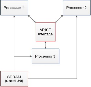
The Proposed Embedded Multiprocessor Architecture uses a new interface called ARISE interface to integrate the Embedded Processors. This is done by assigning one or more pipeline stages of the ARISE Interface to the corresponding pipeline of the processor. In this model, three processors are used with different functions, that is, integer operations, load-store operations and a VLIW (Very Long Instruction Word) processor, which is controlled by SDRAM control unit.
Fig.1.Proposed Block Diagram
The instructions that are executed from the control unit are fed into the processor. The core processor contains a decoder called ARISE Instruction Decoder, which is used to determine the type of instruction that is executed.
IJSER © 2012 http://www.ijser.org
International Journal of Scientific & Engineering Research Volume 3, Issue 1, January-2012 3
ISSN 2229-5518
Instructions are pre-decoded by this Decoder to determine their type (CP or ARISE instructions) and they are issued to the CP or to the interface. Utilizing the Opcode- to-Id Table, the opc field, which has limited bit-width, is assigned to a unique identifier, Id, which can be of arbitrary size. The Id specifies an ARISE operation implemented on a CU (Computing Units). The table also allows the dynamic (at execution time) reassignment of the opc to an Id. Thus, the same opc in an ARISE instruction can be assigned to different ARISE operations alleviating in that way the Opcode space explosion problem. Also, the assignment of opc to ARISE operations is not fixed. Thus, new CUs and ARISE operations can be easily included assigning each operation to an Id. In that way, the modularity and scalability of the machine is enhanced. Since an ARISE operation can be referenced through the opc, which is encoded in the instruction word of the processor, the control communication overhead is minimized.
The IOB provides temporary storage space for the operands of an ARISE operation. It is exploited (through a sequence of move instructions) to support operations with more operands than the CP’s register file provides/accepts per instruction. It is also configured to utilize the complete bandwidth of the register file. Thus, the operand limitation problem is addressed with minimum data communication overhead (without considering the case of increasing the register file ports).
The wrapper controls the configuration and execution of an ARISE operation. It also serves the memory accesses of the CUs through the CP’s memory ports. Moreover, it is used for storing the ARISE configuration bit stream for each operation.
4 ARISE INTERFACE
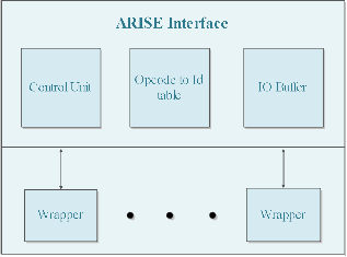
Aristotle Reconfigurable Instruction Set Extension (ARISE) framework is a systematic approach, that is used to extend the processors to support any number and type of computing Units. The ARISE interface has three parts: (1) The control unit, (2) The Opcode-to-Id table, (3) The input/output buffer (IOB).
To incorporate the ARISE interface, the pipeline of the Core Processor is easily integrated with the Pipeline of the ARISE Interface. The interface can stall the CP and block interrupts. To pre-decode an instruction, the Fetch stage of the CP is extended by the ARISE instruction decoder, which produces the ARISE and CP instruction words and forwards them to the PRE and ID stages, respectively. At the PRE stage, based on the received instr value, the ARISE Control Unit generates the control signals for all ARISE components.
Fig.2. ARISE Interface
The Opcode-to-Id table holds the assignment between the opc of an ARISE operation and the unique identifier, Id, of the operation. However, the bit-width of the field is limited. Hence, only a limited number of different ARISE operations can be supported (N operations). To overcome this, the Id value is used to identify ARISE operations. As the Id can be of arbitrary bit-width an “unlimited” number of operations (M operations with N :: M) are supported. To port an operation to the ARISE machine, the designer only needs to associate it with a unique Id. Then, the wrapper is responsible to receive the Id and appropriately control the corresponding CU.
The IO Buffer consists of two register banks. When an ARISE operation needs more operands than the register file provides, a sequence of move instructions (movta, movfa) reads and writes the operands to consecutive places in the banks. The data transfer between the CP and CUs is accomplished utilizing all ports of the register file, which results in fully exploitation of the register file bandwidth. Moreover, since the IOBs operate as pipeline registers, no extra latency is introduced. As a consequence, the operand limitation problem is resolved, while the communication overhead is minimized, under the consideration that the register file ports do not increase.
The wrapper is employed when a new Computing Unit is incorporated. It can be implemented as hardwired unit or hosted on the reconfigurable CU itself. It maps a range of Ids to the corresponding CU. Each ARISE operation implemented by this CU is identified by one of the above Ids. Also, the wrapper is responsible to: (1) Configure the CU and (2) Control the execution of the operations implemented on the CU. To accomplish this, the wrapper includes a table that holds the ARISE configuration bit stream for each operation implemented on the CU. This bit stream is divided into several words. The size of each word equals to the number of bits provided per cycle by the memory.
The Configuration Controller of the wrapper undertakes the control and starts fetching the configuration bitstream from
IJSER © 2012 http://www.ijser.org
International Journal of Scientific & Engineering Research Volume 3, Issue 1, January-2012 4
ISSN 2229-5518
the memory. The words of the bitstream are stored in consecutive (between start and end addresses) places in configuration memory allowing the configuration controller to produce their addresses. The first part of the bitstream is the ARISE configuration bitstream which the Configuration Controller stores in the table. The rest is the configuration bitstream for the reconfigurable CU and it is forwarded to the CU without storing it in the wrapper.
The control the execution of an operation in the wrapper is accomplished by the Execution Controller based on the ARISE bitstream. The Execution Controller performs the following actions: 1) identify if the latency (cycles) of the operation is provided or not; 2) stalls the CP for the number of cycles, if they are provided; otherwise stalls the CP until the CU signals the completion of the operation; 3) sets the ARISE Status Register; and 4) blocks interrupts to CP as it is specified in the ARISE configuration bitstream. Also, the wrapper serves the memory access requests by CUs. Specifically, a CU provides the address of the data memory that needs to access. If the ARISE operation is executed in concurrent mode and the CP has also requested a memory access, the CP is stalled. The corresponding data are directly accessible by the CU. Thus, an ARISE operation can be ported to a CU irrespectively of the implementation technology.
To utilize the CUs, the processor’s ISA is extended once with a set of specific instructions, called ARISE instructions, which control: (1) The execution of the ARISE operations on the CUs, (2) The data communication between the CP and the CUs, (3) The configuration of the CUs. All ARISE instructions have the same format that includes three fields. These fields define: (1) The ARISE instruction (instr), (2) The Opcode (opc) of an ARISE operation, (3) The Operands of the instruction. To extend the CP’s ISA with ARISE instructions these fields are encoded in the instruction word of a CP as shown in Fig.
3. As an example, a processor’s instruction word format is
assumed of which only one opcode, of the available ones of
the CP, is reserved for all ARISE instructions. The secondary
field sec is used to encode both the instr and opc fields, while the operands fields are the same. The operands of an ARISE instruction are accessed via the register file of the CP. It should be noted that the instruction word format in Fig. 3 is typical for embedded processors, like ARM, MIPS, and PowerPC. Therefore, the extension is similarly possible for a wide range of embedded processors.

Fig.3.Encoding of the ARISE instruction word
The interface is organized in a pipeline structure, which was designed to easily extent the pipeline of the CP. Specifically,
in an embedded processor each instruction is executed in three logic stages which are:
� The pre-processing (PRE) stage, where the instructions are decoded and the operands are fetched,
� The processing (PRO) stage, where the operands are processed,
� The post-processing (POST) stage, where the results are send back to the register file.
Similarly, the pipeline of the ARISE interface follows the previous approach. Thus, the ARISE pipeline can be easily integrated to the pipeline of the processor by assigning one or more pipeline stages of the processor to the corresponding ARISE pipeline stage. Thus, the ARISE interface be easily integrated even to processors with deep pipelines.
5 CONCLUSION
Embedded Multiprocessors are used for the areas where fastest calculations, more responsive and performing different tasks are needed. Therefore, an Architecture for Reconfigurable Embedded Multiprocessor had been proposed with the help of ARISE interface using FPGA. With which, Asymmetric multiprocessors can be developed and any number of processors can be added to the core processors using this interface. Bit conversion is also possible between different processors through the ARISE interface.
REFERENCES
[1] Converting Thread-Level Parallelism to Instruction-Level Parallelism via Simultaneous Multithreading. J. lo, S. Eggers, J. Emer, H. Levy, R. Sstamm, and D. Tullsen.
[2] Multiprocessor System on chip Technology, Wayne Wolf.
[3] Design of a Branch Prediction Unit of a Microprocessor Based on Superscalar Architecture using VLSI, Dr. Mrs. Sulabha S. Apte, Ms. Priya P. Ravale, Solapur University.
[4] A reactive multiprocessor architecture for heterogeneous embedded
systems, Zoran Salcic, Dong Hui, Partha S. Roop, Morteza Biglari- Abhari.
[5] A Single-Path Chip-Multiprocessor System, Martin Schoeberl, Peter
Puschner, and Raimund Kirner.
[6] A Complexity-Effective Architecture for Accelerating Full-System
Multiprocessor Simulations Using FPGAs, Eric S. Chung, Eriko
Nurvitadhi, James C. Hoe, Babak Falsafi, Ken Mai.
[7] R. Wittig and P. Chow, “OneChip: An FPGA processor with reconfigurable logic,” in Proc. IEEE Symp. FPGAs Custom Comput. Mach., 1996, pp. 126–135.
[8] F. Sun, S. Ravi, A. Raghunathan, and N. K. Jha, “Synthesis of custom processors based on extensible platforms,” in Proc. IEEE/ACM Int. Conf. Comput.-Aided Des. (ICCAD), 2002, pp. 641–
648.
[9] N. Vassiliadis, N. Kavvadias, G. Theodoridis, and S. Nikolaidis, “A
RISC architecture extended by an efficient tightly coupled reconfigurable unit,” Int. J. Electron., vol. 93, no. 6, pp. 421–438, Jun.
2006.
[10] A. Lodi, M. Toma, F. Campi, A. Cappelli, R. Canegallo, and R.
Guerrieri, “A VLIW processor with reconfigurable instruction set for embedded applications,” IEEE J. Solid-State Circuits, vol. 38, no.
11, pp. 1876–1886, Nov. 2003.
IJSER © 2012 http://www.ijser.org
International Journal of Scientific & Engineering Research Volume 3, Issue 1, January-2012 5
ISSN 2229-5518
[11] Farayadon Karim, Alain Mellan, Anh Nguyen, Utku Aydonat, and Tarek S. Abdelrahman. A Multi-Level Computing Architecture for Embedded Multimedia Applications. IEEE Micro, 24(3):55–56, 2004.
[12] H. Peter Hofstee. Power Efficient Processor Architecture and The Cell Processor. In HPCA ’05: Proceedings of the 11th International Symposium on High-Performance Computer Architecture, pages
258–262, Washington, DC, USA, 2005. IEEE Computer Society.
[13] J. Scott, L. Lee, J. Arends, and B. Moyer, “Designing the low-power
M*CORE architecture,” in Proc. Int. Symp. Comput. Arch. Power
Driven Microarch. Workshop, 1998, pp. 145–150.
[14] N. Vassiliadis, G. Theodoridis, and S. Nikolaidis, “Exploring opportunities to improve the performance of a reconfigurable instruction set processor,” Int. J. Electron., vol. 94, no. 5, pp. 481–
500, 2007.
[15] S. Hauck, T. W. Fry,M.M. Hosler, and J. P. Kao, “The chimaera
reconfigurable functional unit,” IEEE Trans. Very Large Scale
Integr. (VLSI) Syst., vol. 12, no. 2, pp. 206–217, Feb. 2004.
[16] N. Vassiliadis, N. Kavvadias, G. Theodoridis, and S. Nikolaidis, “A RISC architecture extended by an efficient tightly coupled reconfigurable unit,” Int. J. Electron., vol. 93, no. 6, pp. 421–438, Jun.
2006.
[17] H. Singh, M.-H. Lee, G. Lu, F. J. Kurdahi, N. Bagherzadeh, and E. M.
C. Filho, “MorphoSys: An integrated reconfigurable system for dataparalleland computation-intensive applications,” IEEE Trans. Computers, vol. 49, no. 5, pp. 465–481, May 2000.
[18] T. Miyamori and K. Olukotun, “REMARC: Reconfigurable
multimedia array coprocessor,” in Proc. ACM/SIGDA 6th Int.
Symp. Field Program. Gate Arrays (FPGA), 1998, p. 261.
[19] N. Clark, J. Blome, M. Chu, S. Mahlke, S. Biles, and K. Flautner, “An
architecture framework for transparent instruction set customization in embedded processors,” in Proc. 32nd Annu. Int. Symp. Comput. Arch. (ISCA), 2005, pp. 272–283.
AUTHORS BIOGRAPHY

M. Abragam Siyon Sing received his B.E (Electrical and Electronics) Degree from Institute of Road and Transport Technology, Erode - Affiliated to Anna University, Chennai. Currently he is pursuing M.E Degree in Vel Tech Multi Tech Dr.RR Dr.SR Engineering College, Chennai, affiliated to Anna University.
His Area of interest includes Embedded System and VLSI Design.

K. Vidya received her B.E from Vel Sri Rangarajan Sakunthala College of Multimedia, Chennai in 2005 and M.E degree from Sri Sivasubramaniya Nadar College of Engineering, Chennai in 2007. She is currently working as an Assistant Professor in Electrical and Electronics
Engineering at Vel Tech Multi Tech Dr.RR Dr.SR Engineering College, affiliated to Anna University, Chennai. She has 4 years of teaching experience in Engineering College. She has been teaching the subjects: Measurement & Instrumentation and Electrical Engineering. Her area of interest includes
Image Processing and Power System.
IJSER © 2012 http://www.ijser.org