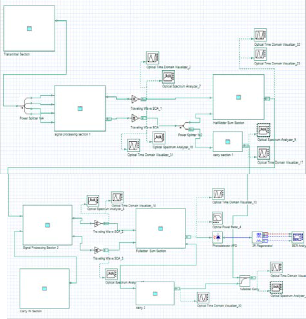
The experimental setup with block diagram for optical full adder is shown in Figure below.
International Journal of Scientific & Engineering Research, Volume 6, Issue 5, May-2015 6
ISSN 2229-5518
Realization of Binary Full Addition Module in
Optical Domain Using SOA
Jaspreet Kaur
—————————— ——————————
inary logic gates are the basic building blocks of the digi- tal logic families like adders, counters, decoders, registers
etc. With the development of high speed optical networks the electronic logic circuits is a challenge in achieving higher bit rate due to the requirement of O-E and E-O conversion. To overcome this challenge the digital logic gates are implement- ed in the optical domain and that can be used in the future for the realization of all the logic circuits in optical domain[2]. The optical logic gates can be designed using the non-linear prop- erties of SOA or using a non-linear fiber. The use of SOA is highly recommended due to its numerous advantages like high gain, high bandwidth along with its coherence and stabil- ity with optical networks. The paper is divided into various sections. Section II describes the advantages of all Optical networks, whereas section III describes the designing and im- plementation of optical logic gates using non-linear properties of SOA. Results and demonstration of setup is explained in section IV.
The purpose of using Optical networks is primarily for the removal of O-E and then E-O conversion. These conversions affect the WDM system more severely as in WDM system for processing using electronic circuitary the wavelength needs to be demultiplexed and a separate transponder is required for every wavelength to convert it into electric domain[3]. These conversions results in increased complexity of the circuit,
power loss and leads to increase cost of the overall system. So to meet the ever increasing demand of higher data rates in communication, optical based circuits will be the future.
Due to the higher potential of optical circuits in computation,
various optical based digital devices has been designed and
proposed like logic gates[1], counters, multiplexer using non- linear properties of SOA.
Working of SOA is based on the principle of stimulated emis- sion where the electrons in the excited state are stimulated to release energy in the form of photons and the process contin- ues until the photons form an amplified signal. This process results in the variation of charge density in SOA. Due to the variation in the charge densities SOA exhibits non-linear properties like FWM and XGM which are used for the realiza- tion of binary logic gates. When two input signals are given to the SOA with difference in frequency less than 6 nm and ratio of signal power to pump power approximately equal to 1, both the non-linear effects i.e XGM and FWM occurs simulta- neously[4].
• Jaspreet Kaur is currently pursuing masters degree program in Electronics and Communication Engineering in Punjab Technical University, India. PH+917837718003. E-mail: jaspreet.12283@gmail.com
————————————————
Truth Table of Full Adder.
When A and B at two different frequencies with different power levels and wavelength difference less than 6nm are giv- en to SOA 1 the Cross Gain Modulation effect gives A(bar)B with input A as high and Input B as low whereas with input A
IJSER © 2015
International Journal of Scientific & Engineering Research, Volume 6, Issue 5, May-2015 7
ISSN 2229-5518
low and Input B high, XGM effect gives AB(bar). The value of XOR gate is high if any of the input is high. When both the inputs are high then the output of AND gate function AB is realized due to the effect of FWM in which harmonic SUM and DIFFERENCE of frequencies are generated. This signal AB is the carry generated by half adder circuit. The signals A(bar)B and AB(bar) are passed through the coupler which at output gives the output of XOR gate as SUM = A XOR B.
The two signals, SUM (S) along with new signal Cin
with different power levels are given to SOA 2, the XGM effect here gives S(bar)Cin with signal S as high and signal Cin as low whereas with input S as low and Input C in as high, XGM effect gives SC in (bar). The signals S(bar)C in and SC in (bar) are passed through the coupler which at output gives the output of XOR gate as SUM (X) = S XOR Cin . This signal SUM is output of full adder.
When both the inputs are high then the output of AND gate function SCin is realized due to the effect of FWM in which harmonic SUM and DIFFERENCE of frequencies are generated. This signal SC in is the carry generated by second circuit. The carry outputs of both the circuits are passed through coupler which gives carry Cout of full adder circuit.
The experimental setup with block diagram for optical full adder is shown in Figure below.
Experimental Set Up
Two CW laser diodes are used to produce two Gaussian puls- es at 1546 nm (Say Signal A) and 1550 nm (Say Signal B) with power 15 dbm & 17dbm respectively. The data input to each modulator is given through a NRZ pulse generator with 10
Gbit/s PRBS data. The modulated signals are then mixed in the
coupler and the signal obtained is amplified by EDFA. A 1x4 power splitter splits the amplified signal into four sections.
The data required is extracted from the four branches with the help of Gaussian optical filters. These signals are passed through attenuators for their optimized power control and are coupled again. The average power of Signal A is
4.413dbm and that of Signal B is 14.262dbm. The signal A acts as probe signal and signal B as pump signal. This attenuated signal passes through SOA 1 and due to XGM property of SOA, function AB(bar) is realised which is extracted with the help of 0.6nm Gaussian optical filter at 1546nm. Similarly in the 3rd and 4th branch the signals A and B after attenuation are set to average powers of 17.435dbm and 3.362dbm respective- ly. Now signal A acts as pump signal and signal B as probe signal. When this signal passes through SOA 2, function A(bar)B is realised which is extracted with the help of 0.6nm Gaussian optical filter at 1550nm. Along with this, a new har- monic component of frequency is generated which realizes the function AB and is filtered by 0.6nm Gaussian optical filter at
1542nm. The information signals AB and AB are combined to perform S =A XOR B. The average power of signals A(bar)B, AB(bar), AB and A XOR B are 11.40dBm, 14.503dBm, -1.00dbm and 14.486dBm respectively.
Now, the output of half adder (Say Signal S) is ob-
tained at frequency 1546 nm and 1550 nm. A frequency con- vertor converts 1546 nm frequency to 1550 nm so as to achieve the output signal at single wavelength i.e at 1550 nm. This output signal S and a generated signal (Say Cin ) at 1546 nm is used as input signals for second half adder circuit. These two input signals are divided into two parts by using a splitter. These signals are again attenuated at different power levels and are then combined through couplers. In first Coupler, the input Cin is at high power of 10.368dBm which acts as pump signal where as input S is at low power of 1.475dBm which acts as probe signal. In SOA 3, the function SCin (bar) is ob- tained due to XGM and is extracted by 0.6nm Gaussian Opti- cal Filter at 1546 nm. Similarly, in second Coupler, the input Cin is at low power of 4.368dBm which acts as probe signal and input S is at high power of 11.475dBm which acts as pump signal. In SOA 4, the function S(bar)Cin is realized due to XGM and is extracted by 0.6nm Gaussian Optical Filter at
1550 nm. On combining these outputs through coupler, output of full adder (S XOR C) is achieved successfully. The output for carry out of full adder is obtained by combining the carry of two half adders.
IJSER © 2015 http://www.ijser.org
International Journal of Scientific & Engineering Research, Volume 6, Issue 5, May-2015 8
ISSN 2229-5518
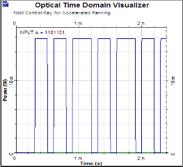
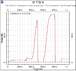
Figure 3. AB = 0101100
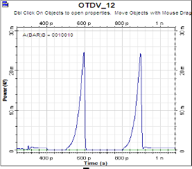
Figure 1. INPUT A = 1101101
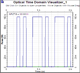 Figure 4. AB = 0010010
Figure 2. INPUT B = 1010011
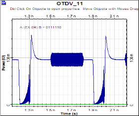
Figure 5. A XOR B = 0111110
IJSER © 2015 http://www.ijser.org
International Journal of Scientific & Engineering Research, Volume 6, Issue 5, May-2015 9
ISSN 2229-5518
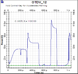
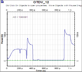
Figure 6. AB = 1000001
![]()
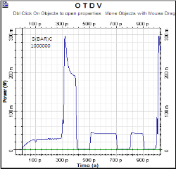
Figure 7. SC in = 1000000
Figure 9. S XOR C = 1100100
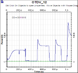
Figure 10. SC in = 0011010
![]()
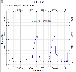
Figure 8. SCin = 0100100
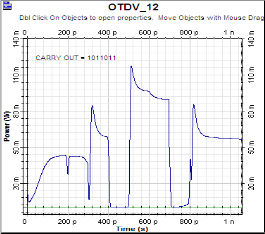
Figure 11. CARRY OUT = 1011011
IJSER © 2015 http://www.ijser.org
International Journal of Scientific & Engineering Research, Volume 6, Issue 5, May-2015 10
ISSN 2229-5518
I would like to thank my parents, friends and teachers for being a constant source of inspiration and support while writing this research paper. Without their help this would not have been a success.
[1] Kristian E. Stubkjaer,” Semiconductor Optical Amplifier- Based All-Optical Gates for High-Speed Optical Processing”, IEEE Journal on selected topics in Quantum Electronics,Vol. 6, No.
6, November/December 2000 A.
[2] A. Teixeira, T. Silveiral, P. Andrd, R Nogueiral, G. Tosi-
Bellefi, P. Monteirol, J. Da Rochal, “All-optical switching with SOA based devices” 12- 17 September2005, Yaya, Cdmea, UkraI- he IEEE.
[3] Adel A. M. Saleh and Jane M. Simmons, “All-Optical Net- working – Evolution, Benefits, Challenges, and Future Vision” Proceedings of the IEEE, vol. 100, no. 5, May 2012, pp. 1105-1117
© 2012 IEEE
[4] Peili li, Xinliang Zhang, Zezhou Zheng and Dexiu Huang, “
Simultaneous demonstration on 10 Gb/s wavelength conver- sion four-wave mixing and cross gain modulation in semicon- ductor optical amplifier” Opitca applicata, Vol XXXIV, No.
1,2004.
[5] S. H. Kim, et al., “All-optical half adder using cross gain
modulation in semiconductor optical amplifiers,” Opt. Express, vol. 14, no. 22, pp.10693–10698, 2006.
[6] S. Kumar, A. E. Willner, D. Gurkan, K. R. Parameswaran, and M. M. Fejer, “All-optical half adder using an SOA and a PPLN waveguide for signal processing in optical networks,” Opt. Express, vol. 14, no. 22, pp. 10255–10260, 2006.
[7] K. Sun, J. Qiu, M. Rochette, L. R. Chen,” All- Optical Logic
Gates (XOR, AND, and OR) Based on Cross Phase Modulation in a Highly Nonlinear Fiber” ECOC 2009, 20-24 September,
2009, Vienna, Austria.
[8] Bo Dai, Satoshi Shimizu, Xu Wang and Naoya Wada, “Simultaneous All-Optical Half-Adder and Half-Subtracter Based on Two Semiconductor Optical Amplifiers” ieee photon- ics technology letters, vol. 25, no. 1, january 1, 2013
IJSER © 2015 http://www.ijser.org