B) The fault cu rrent is reached to speci fied cu rrent level (Id).
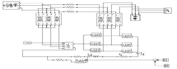
Figure .2 shows the line and DC reacto r cu rrents during first mod e fro m t0 to t4. In o rder to simplify th e analysis, the
Inte rnatio nal Jo urnal o f Sc ie ntific & Eng inee ring Re se arc h Vo lume 3, Issue 3 , Marc h -2012 1
ISSN 2229-5518
Proposed structure of fault current limiter with power quality improvement
L.Karunakar, D.seshi Reddy
—————————— ——————————
Power quality pr oblems are beco ming mo re and mor e i m- portant for utiliti es due to growing nu mber of sensitive loads. Short circuit r esults th e lar ge amoun t of curr ent flow through the distributi on networ k. Th e large fault curren ts flow may damage the series equipment, such as circuit breaker and other system co mp onents. The Fault cur rent causes the vol tage drop of a pa rticular n etwo rk. As a result, some industrial facilities experience produc tion o utage that results in econo mic losses. Ther efore, utilities ar e curr ently exploring mi tigation techniques that eliminate lar ge fault current, increase the reliability o f th e pow er supply and impro ve th e reliability and the system pow er quality. The most co mmon ways to li mit fault cu rrents are the costly replacement o f substation equip ments or impositi on of changes in the configuration splitting p ower system that may lead to d ecreased operational fl exibility and lo wer reliability.
A novel idea is to use Fault Curr ent Li miters to reduce the
fault cur rent to low er, acceptabl e l evel so that the existi ng
switchgear can still be used to pro tect th e p ower grid. An ideal FCL should have the following characteristics
a) Zero resistance/imp edance at no rmal operation ;
b) N o pow er loss in nor mal op eration and fault cases;
c) Large i mpedance in fault condition s;
d) Quic k appearance o f i mpedance when fault occurs;
e) Fast reco very a fter fault remo val;
f) R eliable curr ent li mitation at defined fault curr ent;
g) G ood reliability;
h) Low c ost.
Different confi gurations such as Is - limi ters, solid state
fault curr ent li miters and superconducting fault cur rent
limiters w ere p roposed in previous papers [6] [7] [8]. The SFCL structure o ffers a good way to c ontrol the fault cu r- rent levels in distri bution n etwo rks du e to natural low losses in superconducto rs during the nor mal op eration. Unfortunately, because of high technolo gy and cost of s u- perconducto rs, these devices are no t co mmercially avail a- ble. Therefore, r eplacing the superc onducting coil with nonsuperconducting coil in FCL ma kes it si mpler and much cheaper .
This paper pr oposes magnitud e o f fault cu rrent controlled
by using th yristor circuit of a non super conducting fault limiter . And also i mpro ves the voltage p rofile in a net- work.The circuit op eration in nor mal and fault conditions are simulated and experienced.
The circuit consists of a three phase transfor mer is con- nected to a th yristor circuit at sou rce side. By pro viding the gate pulse to the thyristors to contr ol th e magnitud e of fault cur rent. And another thr ee phase transfo rmer is con- nected to a diode brid ge r ectifi er at load side. Th e di ode bridge recti fier is connected to a parallel connection of a discharging resistor and a thyristo r switch and is connec ted in series with th e D .C reactor is shown in figu re.1.
In nor mal op eration that is without fault conditi on semi- conductor switch is turn on. And r esultant cur rent flo ws through the diod e recti fier and discharging r esistor. And normal cur rent flows to the thyristor circui t. By increasing the inductance value decr eases the ripple o f D .C curr ent. During th e fault condition, the switch is turn on that is when fault take place at load side th en it results th e D .C reactor curr ent increases linearly. If the fault is pres ent for long ti me th e cu rrent thr ough the D.C reacto r will continue to increase. And r esults the source voltage drop take place. There is a control circui t presen t by using that we can con- trol the magnitude of fault cur rent in case of diod e recti fier circuit in previous paper [1]. That c ontrol circuit consists of a discharging resistor and a switch along with resistor. When a fault take place the switch can be turn on and fault current flows to the parallel resistor and it r esults the vol- tage drop take place at sou rce side. In ord er to r educe the magnitude of fault curr ent the switch can be turn-off and the fault curren t flows throu gh the discharging resistor. It results there is a reducti on o f magnitu de of fault cur rent and impro ves th e voltage pro file at source side.
In this paper wi thout using the c ontrol circuit w e can con- trol the fault cu rrent within p rescribed below limi ts. That is in normal operation switch is turn on and normal current flows throu gh the D.C reacto r. In case of fault switch is
IJSER © 2012
Inte rnatio nal Jo urnal o f Sc ie ntific & Eng inee ring Re se arc h Vo lume 3, Issue 3 , Marc h -2012 2
ISSN 2229-5518
turn on then the D.C reactor curr ent increases. To c ontrol the magnitud e of fault curren t by varying the du ty cycl e of thyristor circuit to r educe the magnitud e of fault curr ent in D.C r eactor wi thout using control circuit. Therefor e it i m- proves the voltage pr ofile at source side. Du e to c ontrolling the D .C reacto r cur rent of prop osed NS FCL , it is possible to reduce the curr ent rating of inductance and cancelling out the super c onducting cooling system. Th e co mp ensating voltage pro vided by r ectifi er is
Vc=2vDF+vsw+rdLd (1 )
The circuit has two mod es o f operations a fter fault as fol- lows: A) The fault curren t has not reached to specified cu r- rent level (Id)
B) The fault cu rrent is reached to speci fied cu rrent level (Id).
Figure .2 shows the line and DC reacto r cu rrents during first mod e fro m t0 to t4. In o rder to simplify th e analysis, the
Figure.1 circuit diagram
Turns ratio of an isolation transfor mer is c onsidered equal to one. In this figure, t0 and Ic stand for short circuit instant and specified level for line curr ent, r espectively. In this mod e, the semic onductor switch is closed and w e have two sub-modes as foll ows
a) Charging mod e (betw een t0 and t1 and betw een t2 and t3
in Figure . 2);
b) Discharging mod e (between t1 and t2 and between t3 and
t4 in Figur e. 2).
During charging mode, the DC reactor curr ent is equal to
the line cur rent, and we have the following equation is
Vsinωt+vc=riL(t)+L[diL(t)/dt]+2vDF (2)
Where vc is the compensation voltage and vDF is the vol tage drop across the diod es.
So, the utility and D C r eactor cu rrent equations can be d e-
rived as shown. This equation 2 can be solved by using the steady state and transient analysis![]()
![]()
i (t) =e-(r/L) (t-t0) [i0-(v/z)sin(ωt0- )+ (2vDF-vc)/r ]
+(v/z)sin(ωt- )-[(2vDF-vc )/r ] (3)
Where r = rs + rf + rd
L = Ls + Lf + Ld
iL(t) = id(t) = i (t), z=√r2+(Lω)2 , i0 = i(t0)
Where rf and Lf s tand for res is tance and inductance of fault impedance, res pectively.
During discharging mode, the DC reactor curr ent is more than line current, and the DC r eactor cu rrent fr eewheels through the diod es o f the isolation transfor mer and vol tage transformer recti fiers. In this mod e, we have
Vsinωt=riL(t)+L [diL (t)/dt] (4) Where
r = rs + rf
L = Ls + Lf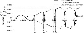
Figure.2 Line and dc reactor current after f ault and before semiconductor sw itch operation
Now line cur rent is
IJSER © 2012
Inte rnatio nal Jo urnal o f Sc ie ntific & Eng inee ring Re se arc h Vo lume 3, Issue 3 , Marc h -2012 3
ISSN 2229-5518
![]()
![]()
i (t) =e-(r/L) (t-t1)[i1-(v/z)sin(ωt1- )+(2 vDF-vc)/r ]![]()
+ (v/z) sin (ωt- ) (5)![]()
z=√r2+ (Lω) 2 , i1 = i(t1), =tan-1(Lω)/r
In addition, it is possible to write the following equation in fault condition and discharging mo de too
Ld (did/dt) +rd id(t) +2vDF-vc=0 (6)
This equation results in the dc r eactor cu rrent for mula gi v-
en as
i(t)= e-(rd/Ld) (t-t1)[i1+(2vDF-vc)/r]-(2vDF-vc)/r) (7)
After t2, w e have another charging mode fro m t2 to t3 and
discharging mod e fro m t3 to t4.
After t4, another charging m ode begins but the line cur rent reaches to specifi ed l evel (Ic ) a t t5 , and it r esults in turn-o ff of the semiconducto r switch by the con trol circuit. N ow,
the discharging r esistor is inser ted in series with th e dc reactor. Fi gure.3 shows the line and dc reacto r cur rent in
this mo de. Fro m t5 to t6, th e line curr ent and dc reactor cu r- rent d ecrease, and we have th e following equation Vsinωt+vc=riL(t)+L[diL(t)/dt]+2vDF (8)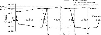
Figure.3 Line and dc reactor current after f ault and semi conductor sw itch
Operation
![]()
![]()
i(t) =e-(r/L ) (t-t5) [i1-(v/z) sin(ω t5- )+2vDF/r ]
+ (v/z) sin (ωt- )-2vDF/r (9 )
Figure.4 Line and DC reactor current after f ault
Figure.4 shows the line cu rrent and DC reacto r cur rent af- ter clearance of fault at t10. During this mode, the DC reac- tor curren t d ecreases because of its discharging r esistor rd, and forward volta ge d rop on diod es. Cl early, by using the superconducting c oil, i ts curr ent also decr eases during the discharging mo de, bu t at a slower rate co mpar ed wi th non- superconducting D C reacto r. Fi g.4 shows that the DC reac- tor cur rent discharges to its pre -fault value that is equal to maximu m of line cu rrent after some milliseconds. In this way, the fault curr ent limiter will be r eady to limi t the next possible fault without any additional pow er or c ontrol ci r- cuit.
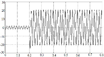
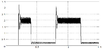
The pow er circui t top ology is shown in figu re.1 is used to simulation. The simulation r esults are obtained NSFCL op- eration per for mance o f a thyristor circuit at a fault condi- tion, where a thr ee phase to ground fault occurs at load side. The neutral of sou rce ground ed. The various op era- tion perfor mances are carried out as follows .The below fi g- ure.5 shows the magnitud e of fault line cur rent, figure.6 shows the D C reacto r cur rent and figu re.7 shows the source voltage drop o f a distribu tion networ k. B y using the thyristor circuit o f applying the suitabl e duty cycl e wi thout turn o ff the switch then th e reduced magnitud e of fault line curr ent is shown in figur e.8, reduced magnitude o f DC reactor cu rrent is shown in figur e.9 and i mpro ved source voltage pr ofile obtained shown in figur e.10. The enlarged
Where![]()
![]()
r = rs+rf+rd+rp L = Ls+Lf+Ld iL(t) = id(t) = i (t)
z=√r2+ (Lω) 2, i5 = i(t5), =tan-1(Lω)/r
The time inter val betw een t5 and t6 is considered as small percentage of power frequ ency p eriod. At t6 the semicon- ductor switch turns on by the contr ol circuit, and we have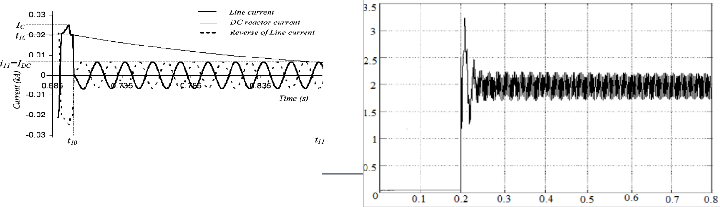
again charging mode until t7. Fro mt7 discharging mode begins and it continues until t8. Fro m t8, another charging mod e begins and it continuous until t9, where semiconduc- tor switch turns o ff to insert the discharging resistor in s e- ries with th e dc reacto r. Th e circuit will have the sa me p e- riodic operation fro m t5 to t9 until clearance of fault
DC reactor curr ent during the fault shown in figu re.11 and
DC r eactor cur rent du ring the transient fault w ere shown
IJSER ©
http:// www.ij
Inte rnatio nal Jo urnal o f Sc ie ntific & Eng inee ring Re se arc h Vo lume 3, Issue 3 , Marc h -2012 4
ISSN 2229-5518
in figure.12.
Figure.10 improvement of voltage profile
Figure.5 magnitude of f ault current
Figure.6 dc reactor current during the f ault
Figure.11 Enlarged DC reactor current during the fault
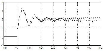
Figure.12 dc reactor current during transient faults
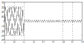
Figure.7 voltage drop during fault
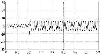
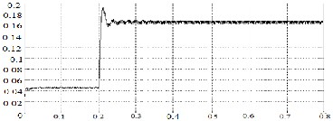
Figure.8 Reduced fault current
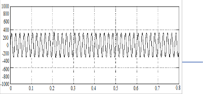
Figure.9 Reduced of dc reactor current
© 2012
ww.ijser.org
Inte rnatio nal Jo urnal o f Sc ie ntific & Eng inee ring Re se arc h Vo lume 3, Issue 3 , Marc h -2012 5
ISSN 2229-5518
The three phase to ground fault is most severe fault in any power sys tem. Whenever it happens to the system th ere is a severe dip in the voltage. This is one o f the power quality problems. T o mitigate the abo ve pr oblem we need to mi- nimize the fault cu rrent. For which in this paper pr oposed fault curren t limiter minimizes th e fault cur rent and i m- proves the vol tage pro file which is obser ved fro m the si- mulation r esult.
[1] M.T Hagh and M.adapour , “ Nonsupe rconducting fault limite r w ith co ntrolling the magnitude s of fault curre nts ,”IEEE Tr ans. Pow er electr onics, vol 24, pp.613-619, Mar ch 2009
[2] E RO Lee, S. Lee, “Test of DC reacto r type fault lim- ite r,” IEEETr ans. Appl. Super cond., vol.12, no.2, mar ch 2002
[3] T.Hoshino, K.M.salim, “ DC rea cto r effect on b ridge type s upe r co nducting fault current limite r,”IEEE Tr ans. Appl. Super cond., vol.11, no.1, pp.1944 -
1947, Mar ch 2001
[4] M. Abapour and M. T . Hagh, “A noncontrol tra ns- forme r inrush curre ntlimite r,” in IEEE Inte. Conf. Ind. Technol., ICIT Sep . 15–17, 2006,pp. 2390 –2395.
[5] M. T.Hagh and M. Ab apour , “ DC rea cto r ty pe tra ns- forme r inrush curre ntlimite r,” IET Elect. Powe r App., vol. 1, no. 5, pp. 808–814, Sep. 2007.
[6] M. Tsuda, Y. Mitani, K. Tsuj i, and K. Kakihana, “Applica tion ofre sisto r base d supe rco nducting fault cu r- re nt l imite r to e nhance ment ofpowe r sys te m trans ie nt stabil ity, ” IEEE T ra ns. Appl. Supe rcond., vol. 11,no. 1, pt. 2, pp. 2122–2125, Mar . 2001.
[7] M. Yagami, T. Mur ata, and J. Tamur a, “ Stabilization of synch ronous gene ra to rs by supe rconducting fault curre nt limite r, ” in IEEE Powe r Eng.So c. Winte r Meet., Jan. 23–27, 2000, vol. 2, pp. 1394 –1398.
[8] Y. Goto, K. Yu kita, H. Yam ada, K. Ichiyanagi, Y.
Yokomizu,and T. Matsumur a, “A study on pow er system tr ansient stability due to intr oduction of super conducting fault cur r ent limiter s,” in Int. Conf.Power Syst. Te chnol., 2000, vol. 1, pp. 275 –280.
L.Karunakar, rec eived B .Tech fro m Prasad v p otlri Siddhartha college of engineering 2008. He has worked as a Lec turer in d epartment of elec trical and electronics in KL university between 2008 to
2010. Present he is pursuing M.Tech in KL Uni ves-
ity. E.mail:lankakarunakar23@yahoo.com
D.Seshi Reddy, r ecei ved B.E and M.Tech fro m Andhra University c ollege o f en gineering And N a- tional Institute of Technolo gy Calicut, India in 2002
And 2004,respectivel y.pr esently he is pursuing ph.d fr om JNT university, h yderabad.
Since 2007, he has been wi th the departmen t of
electrical and el ectr onics engineerin g, kluniversity, where he is curr ently an associate pr ofessor . he has published mo re than ten j ournals and conferences recent tr ends in power system. his cur rent res earch interests include measuremen t of power quality problems, Flexible A C transmission systems.
E.mail: dseshireddy@ gmail.co m
IJSER © 2012