Inte rnatio nal Jo urnal o f Sc ie ntific & Eng inee ring Re se arc h, Vo lume 3, Issue 2, February -2012 1
ISS N 2229-5518
Photolithographic Techniques for LSI and VLSI
M.G. Wani, Dr. V.N.Gohokar
Abstract— Writing the patterns of the Electronics of a digital computer on a minute silicon crystal of 0.2 square inch area.. This thin minute crystal slice
(chip) contains 512,000 transistors other resistor capacitor components. Writing the pattern is just the start subs equent processing involves several other steps.
Index Terms— Optical Lithography, Proximity Pringing, Contact Printing, Projection Printing, Electron Beam Lithography -ray Lithography.
—————————— ——————————
ecent progress in electronics has been mainly in semi- conductor technology particularly in the field of sil icon technology. Here LSI stands for large scale integration
and VLSI for very large scale integration.
These techniques are usually used for increasing the packing
density of the components as well as the functions of the ci r-
cuits on each chip.
The integrated circuit is fabricated by extending the semi-
conductor manufacturing process to include the large number
of transistors on a common substrate in one or more functional circuits.
The monolithic construction as a ‗Single Structure‘ is done by the planer process. Thejunction areas are sensitive to surface exposure and use the inherent protective structure. All diffu- sions take place under a layer of pure Sio2 i.e. silicon dioxide in which the donors and acceptor impurities are introduced to form the NP and PN junction respectively.
In these monolithic integrated circuits both the active and pas-
sive circuits, elements are formed on a single substrate of sil i- con by planner-diffusion technique which involves the combi- nation of photolithography, diffusion, heating and backin g, vaporizing and depositing and ion implantation.
The wafers are obtained by the sequence of so many stages.
The slice of gram ingots of refined silicon sequentially gives
through the following processes Photo Mask, Photo Resist, elements, Diffusion, oxidation lepitaxy, ion implantation and after these molecular processing the circuit metallization by evaporation and sputtering and finally the lead bonding and packaging and encapsulation.
On this silicon slice the same circuitry may be repeated a large
number of times. A silicon substrate chip or slice having size one quarter of an inch contains 250,000 semiconductor com- ponents.
The exclusive costlier IC‘s produces for the defense standards are hermetically (air tight) sealed in dual in line (DIP) or flat Pac ceramic (Cerpac) packages. These devices operationally burned for the 168 hours at 125 o C before delivery to the user.
Resistors are fabricated by (1) omitting N- type emitter-
diffusion used for the formation of transistor (2) Making two
ohmic contacts to a P-type region. That is simultaneously formed with the base diffusion of the transistor. The capacitors are formed by using a top layer of oxide as the dielectric the metalized area as a one plate and N-type material as other plate and the single NP junctions and metalized connection patterns make the diodes.
There is a machine to provide the pins to IC‘s. The name of that machine is KLB-200 i.e. Kellar Machine, Co. Buffalo, New yark. A thick aluminum tape is used in this machine ha v-
ing obedient or complaint characteristics and a clearance for the thin integrated circuits, is super imposed on over this film of Si chip (substrate). Then pressure is applied at the beam leads of the chip and then heated at 300 o C to provide align- ment with the substrate bonding pattern. Due to heating the aluminum yields and flows around the beam lead to enable a reliable and uniform high quality bond.
Since aluminum forms an oxide so there will be no question
of sticking to the internal beam-lead gold contact of the DIP
IC‘s during bonding. The tape is advanced to the next chip by
automatic complaint bonding machine.
For the man production of the LSI and VLSI the following
methods are available.
1) Ultraviolet (UV) optical direct-step on wafer litho-
graphic process or Optical Lithography.
2) X-ray/ X ray imaging.
3) Single and double electron beam or (Electron beam l i-
thography).
The lithographic technique is very old and initially developed by the graphic art industry; just now this technique is used for the manufacturing of the printed circuit boards i.e. (PCB‘s). Recently it is used in the semiconductor electronic industry i.e. for example IC/s production and for it is called as ‗Microl i- thography‘.
By the help of lithography during the fabrication of IC‘s the geometry of microscopic size are obtained. This technique is repeatedly used to sketch or delineate the areas of IC com- ponents in which the diffusion, ion implantation, etching and metallization is done or prevented. This geometric pattern of IC components then transferred to a wafer by direct printing or by a mask. This can be achieved by the etching process.
We know the characteristics of IC to increase the component
density, component speed, delay and minimum line width. Here the line width expected is 0.5 micron and the number of components per IC about 33 millions.
The cost of IC‘s is shared by only this process (i.e. Lithogra- phy) or larges position of the price or cost is shared by Lith o- graphy. About the optical lithography that, by the help of ac- tinic radiation there will be marking of pattern on the resist. Generally this actinic radiation lies between 3800 Ao (violet) and 7800 Ao(red). Resist is nothing but the oxidized silicon substrate coated with photosensitive polymer this is also called as photoresist or resist.
By the help of photomasks we can obtain the multiple layers
of circuit elements geometries.
IJSER © 2012
Inte rnatio nal Jo urnal o f Sc ie ntific & Eng inee ring Re se arc h Vo lume 3, Issue 2, Fe bruary -2012 2
ISSN 2229-5518
The generalized photolithographic system is shown in figure
1.
Now the circuit which is to be replicated is drawn on a thin optically opaque layer (i.e. the substrate which do not allow the light through it) and spread it on a transparent su b- strate like glass. In this way the mask can be produced.
Now after producing the mask the next task to transfer the
pattern of each mask on the wafer surface so as to get the areas
of doping, insulation, contact windows and connection tracks. So to achieve this, the wafer which we previously called as photo resist or resist is coated with light sensitive film. The transfer of the mask to resist surface or wafer is done by ex- posing in light. This resist have tendency to protect the under- lying wafer surface against any chemical or physical a ttack. Just like our PCB manufacturing process. So by exposing in light it is easy as the resist become more soluble in chemical and we can easily remove the unnecessary part of resist which is exposed. Now only the circuit which we want to sketch or draw remains on wafer substrate and it behaves as the stencil for the next processing like etching or metallization.
When the image is exact duplicate of the mask pattern then it is said that the perfect lithographic process is achieved. As the size of wafer becomes small this process becomes less ideal.
The mask exposure can be divided in three parts.
1) Hard contact or contact printing.
2) Proximity printing.
3) Projection printing.
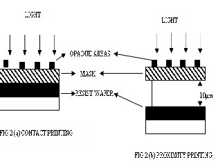
3.1 CONTACT PRINTING
As shown in figure 2(a) is contact printing in which the wafer substrate is bring in physical contact with the mask and then by illuminating or giving light from the back side of mask with actinic radiation. This contact is made by the vacuum
chuck.
3.2 PROXIMITY PRINTING
As shown in figure 2(b) is of proximity printing. While expos-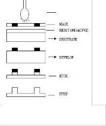
ing the mask to a wafer substrate a finite gap of 10 micrometer is placed between the mask and wafer substrate, so as to re- duce the damages takes place during contact. There are a d- vantages and disadvantages of these methods.
Figure 1. Generalised Photolithographic
System
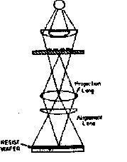
Figure 2 C Projection Printing
![]()
ADVANTAG ES
A) The simplicity and the investment of capital i s less.
B) Good resolution, here the contact printing produces
0.1micrometer resolution while the proximity printing pro-
duces 4 micrometer.
c) The minimum number of optical elements requirement
for the exposure technique and broad band illumination .
DISADVANTAGES
A) The mask life is limited i.e. it depends on the contact of size
of die (stamp).
B) The clamping between two substrates i.e. wafer and mask distorts the wafer surface in an unpredictable manner making it difficult to get repeatable results.
C) Overlay errors as large as 1 micrometer are produced.
D) Highly collimated sources of illumination are used to limit
penumbra effects; the coherency in collimated sources tends to
accentuate effects in the imagery.
The proximity printers operate in the personnel diffrac-
tion region in which the smallest feature achievable is propor-
tional to (λΥ) 1/2, where λ is wavelength of exposing light and Υ is separation between wafer and mask. By decreasing λ we can increase Υ i.e. separation without loss of resolution. But as we know that the operating range of light wavelength is 4000
Ao. If it r educe to 2000 Ao then the mask to wafer separation
can be doubled, which improves the yield. This proximity
printing gives the minimum line width as compared to projec-
IJSER © 2012
Inte rnatio nal Jo urnal o f Sc ie ntific & Eng inee ring Re se arc h Vo lume 3, Issue 2, Fe bruary -2012 3
ISSN 2229-5518
tion printing.
3.3 PROJECTION PRINTING
As shown in figure 2(c), the projection printing can be achieved in order to avoid the damage of mask due to contact printing on the wafer surface the project printing can be used to project the mask on wafer s urface. By use of such printing the resolution will be high than proximity printing and per- mits large separation between mask and wafer. The mask is illuminated and the lens demagnification may vary from 1 to
20 times. This printing depends on the type of lens used (im-
aging) as shown in figure is of simple basic refractive projec-
tion mask aligner. ADVANTAGES:-
A) Non contact operation which prevents the mask
wearing and tearing defects.
B) Cost of masks, it saves the replacement of more masks.
C) Uniform images:- as single mask is used we set the
wafer images more uniform.
D) No need to move the wafer after alignment.
E) The mask can be easily fabricated and easily repaira- ble.
F) By using reduction lens the head size becomes smal l- er than wafer and the step and repeat operation is ne- cessary to cover the entire wafer.
DISADVANTAGES:-
A) Complexity and higher cost of projection lens, the re-
fraction lens of one or two wavelengths are used.
B) Standing waves produced on photoresist image caus- es the maximum line width i.e. width control is more difficult.
But these printing methods are common in practice in IC
manufacturing for years. Now a days X-ray lithography is used. X-ray whose wavelengths are 4 to 50 Ao are useful for X-ray lithography, by means of which all the above three disadvantages cab be overcome.
When electron from the electron gun strikes the target, then there is ejection of electrons from the inner most shell of target atom and creates vacancy which is then filled by electron from the higher energy level. When the electron moves from higher energy level to inner lower energy level it losses its energy and this energy appears in the form of electromagnetic radiation. The energy of this electromagnetic radiation is equal to the difference of the two energy levels. the form of X-rays. These X-rays can be emitted at As this energy is large in the inner shells, so this is different energies (depending on the donor shell level energy).
The wavelength of X-ray is in the range of 0.05Ao to 100 Ao. The X-ray having the spectrum from 4 to 50 Ao is called soft X- ray and are useful for X-ray lithography, as shown in figure 5 is the X-ray exposure system.
A] GENERATION OF X-RAYS:-
X-rays are generated in an evacuated area by accelerating electrons (from few KeV to tens of keV) from a heating fila-
ment to heat the metal anode(farget) made of sya, tungsten, ionizing some of the atoms by inelastic scattering of inner shell electrons. The excited atoms of the target decay to ground state passing through intermediate steps loosing energy at each step. In some steps, this decaying energy produces X - rays whose wavelength depends on atoms energy level before and after the step. Additionally when electrons are decelerated by the target atoms they radiate energy in the form of conti- nuous X-rays.
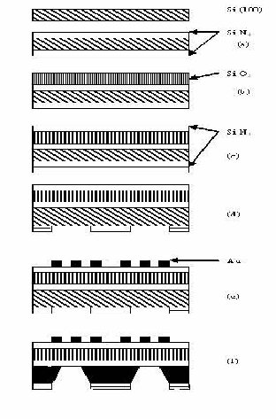
B] PREPARATION OF X-RAY MASKS:-
One of the key factors in x-ray lithography is the construction of mask. The mask essentially consists of absorbing patterns over a thin film or transparent material. The membrane of is usually a few micron thick (Generally membrane is of chro- mium).
This membrane should be flat, smooth, sell supporting, di-
mensionally stable and mechanically tough to withstand the handling hazards during fabrication. The membrane should also be optically transparent s o that optical mask alignment procedures can be used. The thermal expansion properties of the mask and wafer must match photoelectrons generated on the mask materials should be prevented from reaching and exposing resist. These masks can be of organic or i norganic materials. Organic membranes are superior in flatness, smoothness has high chemical resistance and dimensional stability but poor in strength, so the size of them is limited (about few mm square). On the other hand organic materials may be polymer films like Mylar or polyimide while inorganic materials may be films of Si3N4, Al2O3, Sic etc. the membrane may be also combination of organic and inorganic films such as BN/Polyimide. The steps of X-ray mask fabrication by us- ing inorganic materials are shown in figure 5.
System Architecture:- Schematic diagram of EBL for direct writing on wafers is shown in figure4. This system, developed by Hewlett Packard, consists of an electron column, a target area with a cassette loading system, an X-ray stage, a comput- er control system, and a variety of special purpose electronic equipment used to drive the beam and control the data. At the top of the column is the field emission electron gun which is capable of producing high current densities. It consists of tungsten cathode and an accelerating anode (second anode). The cathode is operated at 20 KeV with respect to second anode, providing a field of approximately 2×10 7 V/cm at the tip of cathode. Emission from cathode is control led by first anode placed just around and above the cathode tip. A voltage of around 3 to 4 KV is applied to this electrode, to produce change in field at the tip hence control the emission. This con- trol electrode is also called as schottey shield.
The beam formed by emitted electrons passes
through the first lens and is focused near a knife edge in the beam blanker region.
A] BLANKER SYSTEM
To achieve patterning of the wafer or mask the beam must
IJSER © 2012
Inte rnatio nal Jo urnal o f Sc ie ntific & Eng inee ring Re se arc h Vo lume 3, Issue 2, Fe bruary -2012 4
ISSN 2229-5518
be turn on and off at a rate much faster than the data rate of say, 300 MHz. This is achieved by a beam blanker system. The blanker system provides the high speed intensity modulation of the electron beam necessary to writ patterns as the beam is moved across the wafer or mask in a raster scan mode.
In the blanker system the beam is focused just to the side of a knife edge. When a potential of about 3 volts is a pplied to the blanker, the beam is deflected a few micron and strikes a knife edge of a metallic plate. The electron are there by stopped from reaching the target. The design uses an electros- tatic defection system. To facilitate stationary blanking the blanker plates are positioned symmetrically about across over. In the region of the first lens, there is a system to correct bea m is also an alignment coil for the compensating column misa- lignment.
The final lens forms an image of the blanker cross over on to
the target plane. Immersed in the final lens are final astigma-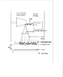
tion and alignment coils which focus the beam on the target. Beam focus is adjusted by means of a small dynamic focus coil buried in the middle of the final lens.
Figure 3 Schematic of a X-ray exposure
System
B] DEFLECTION SYSTEM
Following the final lens is the deflector system consisting of
Quadra pole deflection and Octopole deflection . The upper
deflector, a Quadra pole is used to raster scan the beam rapi d- ly over a limited area of 64 micron square field.
The lower deflector, an octopole or eight fold deflector is
situated in the field free region and provides a precisely con- trolled field distribution. The octopole can scan a full 5 mm square field.
C] X-RAY STAGE AND SUBSTRATE HANDLING SYSTEM
The ability to position the substrate according to the area be exposed is crucial to the performance of an electronic beam
lithographic system. This is done by an X-ray stage which has a very precise mechanism controlled by a laser interferometer and servo systems.
When a wafer is loaded into the system, specific wafer data are supplied to the computer in what is called the wafer map. This contains the parameters for use by the control and data editing programs in adjusting the system to the unique re- quirements of the wafer to be written.
To facilitate automation of the registration process without using very large registration marks on each chip, a three step process is used. Mechanical alignment, wafer registration, and chip registration.
First, an automated mechanical handler loads the wafer
onto the carrier. Then the wafer carrier is introduced in to the vacuum chamber by means of an interlock system, and placed on an X-ray table, which positions the wafer under neath the electron beam.
Second, the beam scans wafer registration marks to sense the
errors in position, magnification and rotation. To detect the
beam as it scans the targets, there is a system of four detectors near the target area corresponding to the plus and minus of X and Y axes. The targets are made of scintillating material that emits light when struck by back scattered electrons. A pipe routes the light to a set of photomultiplier tubes which convert the weak light into large electrical signals.
After the final lens the beam goes to the target through a double vacuum valve. The valve allows the column to split open while maintaining vacuum both on the gun side and lower section of the Coolum. This facilitates the installa- tion on a new gun or change of wafer without affecting each other.
The third and last step is chip registration for which fudi- cial marks as shown in figure at the corn ers of each pattern area are used. The electron beam is used as a probe similar to that of scanning electron microscope. The fudicial marks are scanned, the errors detected and corrected as the pattern is written.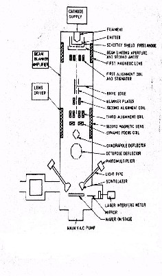
Figure 4 Schematic diagram of Electron Beam Lithography
IJSER © 2012
Inte rnatio nal Jo urnal o f Sc ie ntific & Eng inee ring Re se arc h Vo lume 3, Issue 2, Fe bruary -2012 5
ISSN 2229-5518
oxide, and silicon dioxide most manufactures uses tantalum for resistor and capacitor fabrication, by photo etching pa t- terns of sputtered tantalum film over the substrate. The film is then oxidized to the desired depth to form the dielectric for capacitors. Gold or platinum deposits then make the condu c- tion electrodes and interconnections.
The ceramic alumina (0.5 inch by 60 mis thick) is typical sub- strate of thick-film fabrication technique. The thick films are applied to the substrate by the silk screen process. A meta l- lized ink interconnection patterns by the silk-screen process if followed by firing at 700 oC resistors are formed by us ing a metal glass slurry via the silk screen process and the desired patterns firing is repeated. Capacitors are often miniature components soldered or welded into the circuit for higher va l- ues; films are fabricated on the substrate for low values. Dep o- sited ceramic and glass paste makes the dielectric. After firing, a top electrode of platinum is applied. The inter connection pattern is coated with 2 to 3 mils of solder. The passive com- ponents (in both thick and thin films) can be dynamically trimmed by laser techniques for close tolerances as 0.05 to
0.001 percent.
8 CONCLUSION
Photolithographic technique is the best method for the fabrica- tion of thick and thin films, as well as for the manufacturing of Integrated Circuits.
Figure5. X-ray mask fabrication steps
which convert the weak light into large electrical signals.
After the final lens the beam goes to the target through a double vacuum valve. The valve allows the column to split open while maintaining vacuum both on the gun side and lower section of the Coolum. This facilitates the installation on a new gun or change of wafer without affecting each other.
The third and last step is chip registration for which fudicial
marks as shown in figure at the corners of each pattern area are used. The electron beam is used as a probe similar to that of scanning electron microscope. The fudicial marks are scanned, the errors detected and corrected as the pattern is written.
A substrate wafer of silicon dioxide is used with a 0.25 to 1 inch square area. Thin films, with a thickness from 0.1 to 0.001 mil, are deposited by evaporating or sputtering methods. Thin film resistors of values of 10 to106 ohms are fabricated by eva- porating nichrome or tantalum form strips between terminals, the value is controlled by composition of the film used, and its length, width and thickness. Thin -film capacitors are fabri- cated by applying the requisite conducting areas to both sides of thin-film of dielectric such as tantalum oxide, aluminum
[1] D.H. Scheiber and R. M. Rosenberg, ― Circuitry from Phot oprintable Paste; A New Technology,‖ in Proc. 1972 Int. Microelectronics Symp., p. 4-A-3-1.
[2] D.H. Scheiber and R. V. Weaver, ― Circuitry from Phot oprintable
Pastes: FODEL Photoprintable Dieletectric Composition.‖ in P roc.
1973 Int. Microelectronic Symp., p. 3A – 3 -1.
[3] D. M. Gibson, ― A Method for Thick Film Printing of Conductor Fine
Lines and Spacing,‖ ISHM‘77.
[4] L. R. Fletcher, ― Thick – Film Applications in Hybrid Microwave Substate Fabrication,‖ preseted at the 1976 Int. Microelectronics Symp.
[5] R. P. Mandal,‖ Evaluation of Advanced Microelectronic Flu xless Solder Bump Contacts for Hybrid Microcircuits,‖ NASA Contractor Rep. NAS 8-3 1496, June 1970.
[6] Electronics for you. July 1986 to October 1986.
[7] Guthikonda V. Rao., Microprocessors and Microcomputer Systems., (IInd edition)
IJSER © 2012