International Journal of Scientific & Engineering Research, Volume 4, Issue 9, September-2013 1947
ISSN 2229-5518
Performance Evaluation of Microwave Transistor
Amplifiers
Animesh Kopekar is currently pursuing master’s degree program in Communication Engineering at Manchester University, UK.
E-mail: askopekar@gmail.com,
Atul Dhakate is M. Tech (Signal Processing) from VIT, Pune and currently working as a Lecturer at RGCER of RTMNU.
E-mail: atul.dhakate@hotmail.com
Bhavna Kohachade is B. Tech from Dr. Babasaheb Ambedkar Technological University, Raigad Mumbai Goa highway.
E-mail: bkohachade@gmail.com
Abstract — Microwave transistors are useful as small-signal amplifiers to 6 GHz and power amplifiers to 4 GHz. Nearly all microwave transistors are of the silicon planar type. Power transistors uses three types of geometries- interdigitated, overlay, and mesh-while small- signal transistors use interdigitated only. The general theory of the frequency response of transistors is reviewed, including active and inactive elements. A condensed description of the design and processing steps for a silicon microwave transistor is given. A final section deals with the types of high-frequency measurements used in the design and analysis of transistors. The characterization of active microwave devices and design of the wide-band microwave amplifiers are among major interests in communication engineering. Especially in designing microwave amplifiers, many sophisticated numerical methods are utilized to optimize system performance. Generally, the optimization is focused on the transducer power gain (G T ) over the frequency band of operation without controlling the other performance criteria such as the noise (F), the input voltage–standing wave ratio (VSW R, Vi ), and the output VSW R (Vo ). It should also be mentioned that the optimization process of the performance is highly nonlinear in terms of the descriptive parameters of the system. Certainly, within the optimization process, one can easily embed the desired performance goals without knowing the physical limits and/or compromise relations among F, V i , and G T appropriately. Unfortunately, this process often fails to attain the desired goals. However, the complete performance characterization of a microwave transistor overcomes all the above-mentioned handicaps. In this work the upper (G T max ) and lower (G T min ) gain bounds are easily obtained for the chosen noise F, F min and V i pairs point by point in the operation domain of the transistor. Furthermore, one can have all the interrelations among the performance.
Index Terms— Ideal amplifiers Short circuit parallel stub with series transmission line, quarter wave transmission line transformer with series transmission line, quarter wave transformer with parallel open circuit stub, Micro Strip Narrowband Amplifier, Micro Strip Broadband Amplifier.
1 INTRODUCTION
—————————— ——————————
N this laboratory section, two different types of amplifiers will be designed using Advanced Design System (ADS) software. First is the micro strip narrowband max transduc-
er power gain amplifier, which can only increase the magni- tude of signals over a small frequency band compared to the average frequency of the signal band. The second one is the micro strip broadband constant transducer power gain ampli- fier, which has a flat response over a wide range of frequen- cies. It is used in for transmission of signals like AM and FM or more precisely for transmission of signals in radio transmit- ters for communications between telecommunications towers. Focusing attention on transistor tuned amplifiers and their increasing applications in high frequency electronic circuits. Main purpose of this lab was to design the input and matching stages of an amplifier. This was done at a center frequency of
4MHz.
2 THEORY
Stability in referring to amplifiers means an amplifier's im- munity to causing spurious oscillations (Microwave101, 2013). Conditional stability is defined that the amplifier stays stable only with particular impedances, which means that there is a region of either source ( | Γin | < 1 ) or load impedances ( | Γout | < 1 ) that will definitely cause it to oscillate. Uncondi-
tional stability means that the amplifier is stable with any im- pedance ( | Γin | ≤ 1 ) and ( | Γout | ≤ 1 ).
The stability factor, K, of an amplifier is a one scalar dimen- sionless quantity that is the most valuable measure of stability for a given frequency. If K-factor is greater than one tells that the amplifier is ‘unconditionally stable’. And if K is less than 1, the amplifier may have a problem in some frequencies. Below is the equation 1 for K-factor.

1 − |𝑆11 |2 − |𝑆22 |2 + |Δ|2
𝐾 = 2|𝑆 𝑆 |
𝑎𝑛𝑑
Δ = 𝑆11 𝑆22 − 𝑆12 𝑆21 (1)
The maximum available gain (MAG) of a device is only de-
fined where K < 1, which is the maximum available average
power at the load over the maximum available average power
from the source (Wikipedia, 2013a). The equation below shows
IJSER © 2013 http://www.ijser.org
International Journal of Scientific & Engineering Research, Volume 4, Issue 9, September-2013 1948
ISSN 2229-5518
how MAG is calculated from stability factor K and the for- ward and reverse transmission coefficients:
determined with the help of the S-parameter measuring de- vice. S-parameters are being found out. The frequency range

𝐺𝑀𝐴𝑋 = �𝐾 − √𝐾 2 − 1� ×

|𝑆21 |
|𝑆12 |
𝑓𝑜𝑟 𝐾 > 1
To achieve MAG, the power transfer should be maximized, which means minimizing reflections from the load. So we should match the input and output of the amplifier to the source and load. In electronics, impedance matching is to de- sign the input impedance of an electrical load or the output impedance of its corresponding signal source to maximize the power transfer or in other words, minimize reflections from the load (Wikipedia, 2013b). In the laboratory work, transmis- sion lines, open circuits stub and short circuits stub are used to make the amplifier match to 50Ω using Smith chart.
The Smith chart is plotted on the complex reflection coefficient plane in two dimensions and is scaled in normalized imped- ance. The Smith chart can also be used to simultaneously dis- play multiple parameters including impedances, admittances, reflection coefficients, S-parameters, noise figure circles, con- stant gain contours and regions for unconditional stability, including mechanical vibrations analysis (Pozar, David M.
2005).
3. PROCEDURE
3.1 General Test
In this part, three ideal matching circuits, short circuit parallel stub with series transmission line, quarter wave transmission line transformer with series transmission line and quarter wave transformer with parallel open circuit stub will be simu- lated and their performances will be compared.
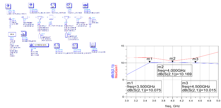
The device used in this laboratory is Fujitsu C-Band Power GaAs FET, FLC317MG-4. Put it in a testing circuit as shown in Figure 1 below.
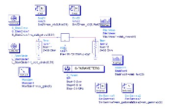
Figure 1: Device Under Test
In the above figure 1 it can be observed that the amplifier for narrowband is being observed. S-parameters are being
in which are found out is from 2 GHz to 6 GHz. Also stability factor and stability measure are being found out with the help
of simulation S-param palette as StabFCT and StabMs.
Figure 2
Figure 3
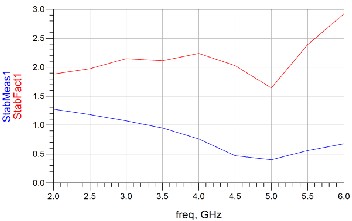
The stability of the device should be tested firstly. As can be
seen in Figure 2, from 2 GHz to 6 GHz the stability factor is
always >1 and the stability measure is >0. So we can conclude
from figure 2 and 3 below that within this frequency band, the
device is unconditional stable.
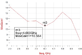
Then with the result of maximum gain from Figure 2, the cen- tral working frequency of the amplifier is set to be 4 GHz be- cause the value of maximum gain at this frequency is accepta- bly lowest during this frequency band so that the device can work well at other frequencies nearby as well.
IJSER © 2013 http://www.ijser.org
International Journal of Scientific & Engineering Research, Volume 4, Issue 9, September-2013 1949
ISSN 2229-5518
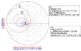
Figure 4: Stability Circles
We can see from the Figure 2 above that the K > 1 and b > 0.
From the Figure 4 the stability circles can be observed and the load and source circles are plotted and stability is observed for the circuit built up.
With the help of Function SmZ1 and SmZ2, the simultane- ous input and output matches achieving the maximum gain were calculated respectively as 32.264-j57.757 and 14.160-j4.850 at 4 GHz.
With the Smith chart shown in Figure 8, the parameters of the transmission lines and the open circuits for the amplifier are decided.
3.2 Performances
Here are the plots of S (2, 1) and maximum gain against fre- quency of the three amplifiers shown in Figure 5, 6 and 7.
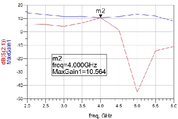
Figure 5: Performance of short circuit parallel stub with series transmission line
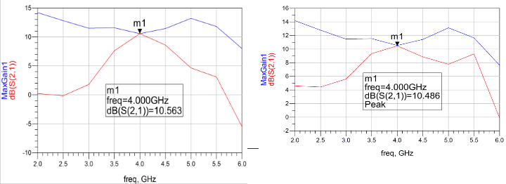
Figure 6: Performance of quarter wave transmission line trans- former with series transmission line
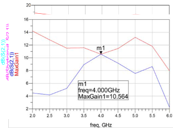
Figure 7: Performance of quarter wave transformer with paral- lel open circuit stub.
Figure 8: S21 Parameters comparisons of all methods with the
Ideal Gain.
As can be seen in the Figure 8, that the maximum S (2, 1) of the three circuits are all 10.564 dB. So a conclusion can be drawn that the performance of quarter wave transformer with parallel open circuit stub. It is better than the other two ampli- fiers because S (2, 1) and maximum gain are close to each other near 4 GHz, which means that the amplifier has a wider bandwidth. So the matching circuits for quarter wave trans- former with parallel open circuit stub are chosen for the de- sign of the micro strip narrowband amplifier in the next part.
3.3 Narrowband Amplifier
In order to design the micro strip narrowband max trans- ducer power gain amplifier, the ideal components should be equally changed into micro strips (practical) component. With the help of calculation tool in ADS, the values of impedance and electrical length are easily turned into the width and length of the micro strips.
Figure 9: Micro Strip Narrowband Amplifiers.
R ©
ww.ij
Int eptember-2013 1950
ISS
Figure 13: Ideal Broadband Amplifier
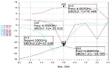
Figure 10: Performance of Narrow Band Amplifier using quarter wave transformer with parallel open circuit stub
Figure 11: S-parameters for the Narrow Band Amplifier. The micro strip narrowband max transducer power gain
amplifier is built as shown in Figure 9. The bandwidth of the
circuit comes out to be 10.486 dB from figure 10. We can see
there are very less losses at 4GHz as shown in Figure 11. This
shows that the circuit is matched properly.
3.3 Broadband Amplifier
The broadband amplifier requires that the amplifier has 10 dB flat gains in a large frequency band which is 3.5-4.5 GHz.
First, draw a 10 dB gain circle on the Smith chart. Assume that the output is conjugated matched. The line conj(s(1,1)) makes crossover points with the gain circle as shown in Fig- ure13. Read the value of the impedance of the point that is nearest with the origin, which is 67-j4985. Try to match this impedance to the source with quarter wave transformer with parallel open circuit stub. Matching circuits on Smith chart as shown in Figure 12.
Figure 12: Matching with the Smith Chart
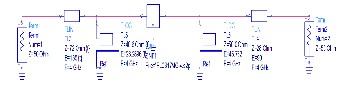
Figure 14: Performance of Broadband Amplifier using quar- ter wave transformer with parallel open circuit stub
We tune the circuit in fgure 13 to get the figure 14. As can be seen from Figure 14, the S (2, 1) is nearly constant around
10 dB than which the maximum gain is only a higher during the frequency band from 3.5 GHz to 4.5 GHz. The bandwidth of this amplifier is much wider than the ideal narrowband amplifier. Also from the plot can be seen that S(2,1) is larger around 4.7 GHz, which means the amplifier has a better per- formance at that further frequency also.
Convert the matching values into micro strip width and length and form the whole amplifier circuit. Run the simula- tion and use tune tool to adjust the performance of S(2,1) to achieve the requirement.
4 RESULTS
4.1 Narrowband Amplifier
As can be seen from the plot below, S(2,1) is nearly reach the maximum gain of the device and is not so sharp which means
IJSER ©
http://www.ij
International Journal of Scientific & Engineering Research, Volume 4, Issue 9, September-2013 1951
ISSN 2229-5518
that, comparatively speaking, the amplifier has a large band- width.
REFERENCES
[1] En.wikipedia.org (n.d.) Impedance matching - Wikipedia, the free encyclopaedia.
Figure 15: Performance of Narrowband Amplifier
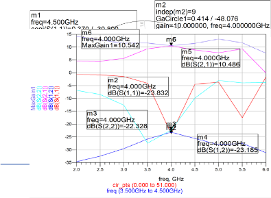
For the micro strip narrowband max transducer power gain amplifier, the bandwidth is not large as the maximum gain at
4 GHz i.e. 0.1dB less. As can be seen from above Figure 15 there is slight variation in the ideal and the practical mi- crostrip cases (Shown by marker m5 and m6) the values are nearly the same but differ slightly. The other parameters like return loss is given by S (1, 1). It can be seen from the plot that the there is more losses in the lower frequency and low losses at the 4 GHz frequency i.e. it shows it is perfectly matched. Further the losses vary accordingly.
4. 2 Broadband Amplifier
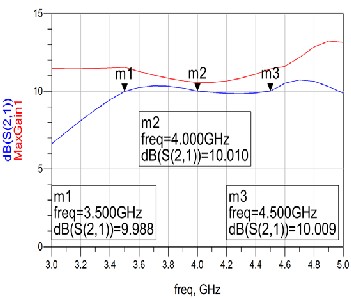
As can be seen from Figure 16, the S (2, 1) is nearly constant around 10 dB than which the maximum gain is only a higher during the frequency band from 3.5 GHz to 4.5 GHz. The bandwidth of this amplifier is much wider than the narrow- band amplifier. Also from the plot can be seen that S (2, 1) is larger around 4.7 GHz, which means the amplifier has a better performance at that further frequency also.
Figure 16: Performance of Broadband Amplifier
5 CONCLUSION
Comparing the ideal amplifier with the microstrip amplifier, conclusion can be drawn that there is a small difference in the performance between them. If we compare the S(2,1) parame- ters of the two circuits we can see that in the ideal case, S(2,1) can reach the maximum gain. However, in the microstrip case, the value are slightly changed due to the components like mi- cro strip and the T-junction used in there.
For the micro strip narrowband max transducer power gain amplifier, the bandwidth is not large as the maximum gain at
4 GHz i.e. 0.1dB less. It is relatively low. As can be seen from Figure 20 there is slight variation in the practical microstrip cases as compared to ideal (Shown by marker m5 and m6)
S-Parameter S (1, 1) gives us the return loss, i.e. - 23.8 dB is the lowest at 4 GHz, which means that the circuit is well matched. For the microstrip broadband constant transducer power gain amplifier, the band width is wider because S (2, 1) is constant- ly 10 dB from 3.5 GHz to 4.5 GHz. It reaches the maximum gain during this specified frequency band. The return loss may not be good at 4 GHz due to the tuning of the circuit. The return losses are around-9.70 dBm, but it is good somewhere after 4.5 GHz that is after working frequency band.
After all, on the condition of stability, we see that the design- ing of amplifiers mainly depends on the maximum gain and S (2, 1) plot of the device. With the specified matching technic of the transmission line, the amplifier can be designed to achieve special requirements of the users.
[online] Available at: http://en.wikipedia.org/wiki/Impedance_matching
[Accessed: 10 Mar 2013].
[2] Microwave101,AZ, P. (2011) Stability factor - Microwave Encyclopedia - Microwaves101.com. [online] Available at: http://www.microwaves101.com/encyclopedia/kfactor.cfm [Ac- cessed: 10 Mar 2013]
[3] Pozar, D. M. (2005). Microwave engineering. Hoboken, NJ, J. Wiley. pp
64-71.
[4] J.S. Kenney, and A. Leke, “Power Amplifier Spectral Regrowth for Digital Cellular and PCS Applications,” Microwave Journal, vol. 38, no.10, pp.74-92, October 1995.
[5] M.S. Muha, C.J. Clark, A.A. Moulthrop, and C.P. Silva, “Validation of Power Amplifier Nonlinear Block Models,” 1999 IEEE MTT-S Inter- national Microwave Symposium, 1999, pp.759-762 vol.2.
[6] Computer.org. 2004. Microwave engineering education over the web.
[online] Available at:
http://www.computer.org/csdl/proceedings/fie/2012/1353/00/06
462207-abs.html .
[7] http://www.ieee802.org/. n.d.. POWER AMPLIFIER MODEL PA- RAMETERS. [online] Available at: http://www.ieee802.org/16/tg1/phy/docs/802161p-00_09r1.pdf.
[8] Toronto.ieee.ca. 2005. IEEE Toronto Section - Events. [online] Availa-
ble at: http://toronto.ieee.ca/events/jun2205.htm.
[9] www.ieee.org. n.d. Phase Noise in RF and Microwave Amplifiers. [online] Available at: http://www.ieee-uffc.org/frequency- control/learning/pdf/Rubiola- Phase_Noise_in_RF_and_uwave_amplifiers.pdf.
IJSER © 2013 http://www.ijser.org