INTRODUCTION
T
HE increasing market of mobile, hand-held devices and battery powered portable electronic systems as well as the increase in data transfer rates demands that these
systems use less power and reduce operational delays.
These devices and systems demand high-speed, high- throughput computations, complex functionalities and often real time processing capabilities. The performance of these devices is limited by the size, weight and lifetime of batteries. Serious reliability problems, increased design costs and battery operated applications prompted the IC design community to look more aggressively for new approaches and methodologies that produce more power efficient designs, which means significant reductions in power consumption for the same level of performance. Since memory currently makes up a large part of systems, nearly fifty percent, reducing the power and delay in memories becomes an important issue.
This paper explores the design and analysis of Static Random Access Memories (SRAMs), focusing on optimizing delay and dynamic power. Memory access incorporates two different operations: the memory read and the memory write. Owing to high bitline voltage swing during write operation, the write power consumption is dominated the dynamic power consumption. To improve the performance of the memory write operation different cell designs are suggested by variations in basic 6T SRAM cell. Since short-circuits are responsible for much of the dynamic power loss, concept of virtual source transistors is used for removing direct connection between VDD and GND. Faster write time can be achieved by using transmission gates instead of simple NMOS pass transistors.
————————————————
By implementing these improvements four different memory cell designs are proposed. Each of these designs has been extensively simulated in 16nm CMOS predictive technology. Simulation results indicate similar type of outputs for same input while working with these designs but power dissipation and delay has significant changes with varying schemes.
Secondly the technology is also scaled down to 16nm so
power and speed is also optimized accordingly for future
scope of designing [1]. Besides these factors, very small device dimensions show a remarkable area reduction, which is also an added advantage [2].
A family of SRAM cells is designed for removal of wasteful sources of dynamic power consumption that result from short circuits that exist when the memory cell is switching. The performance of each cell structure is determined by comparing power and delay performance of these structures.
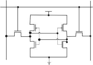
STANDARD 6T SRAM CELL ARCHITECTURE
The mainstream six-transistor (6T) CMOS SRAM cell is shown in Fig. 1. Similar to implementations of an SR latch, it consists of six transistors [3]. Four transistors (Q1 − Q4) comprise cross-coupled CMOS inverters and two NMOS transistors Q5 and Q6 provide read and write access to the cell. Upon the activation of the word line, the access transistors connect the two internal nodes of the cell to the true (BL) and the complementary (BLB) bit lines.
BLB BL
WL
Q3 Q4
Q5 Q6
Q1 Q2
Fig. 1: Six Transistor (6T) CMOS SRAM Cell
PROPOSED CELL DESIGN
Schematics of all proposed cell is designed at 16nm technology so minimum sized transistors are used according to that i.e. L is taken to 16.5nm and W is varied to satisfy the size constraint of SRAM cell [4].
8T SRAM Cell with CMOS TG access Transistor (TG SRAM 8T)
In standard 6T SRAM cell one internal node cannot completely attain a logic ‘1’ value until another node fully discharges its capacitance and turns on transistor to supply full VDD to first node and vice-versa. A solution to this problem is to add two pMOS pass transistors to each memory latch i.e. in place of nMOS access transistors CMOS transmission gates can be used as shown in schematic of Fig.2. Ideally, this will produce faster write times since both a strong ‘1’ and ‘0’ will simultaneously be written to the memory [5].
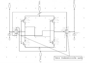
Fig. 2: Schematic Designing of TG SRAM 8T
This should lead to the added benefit of reduced dynamic power dissipation within the memory cell because of the shorter switching time for the cross coupled inverters, which
means less time for a short circuit to exist. However, it is important to remember that the additional pMOS transistors will also lead to greater capacitances on the bitlines, and therefore greater power consumption and slower bitlines switching speeds.
8T with TG access and Virtual GND Transistor (VGc)
By insertion of nMOS transistor (Virtual GND Transistor TVG) as shown in Fig. 4.6, between GND and the source contacts of nMOS transistors N3 and N4 [6]. As the short circuits terminate at the GND source contact in each memory latch, the addition of TVG is an effective way to eliminate it simply by turning TVG off through a control signal VSn.
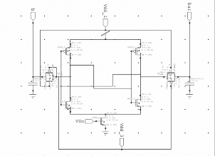
Fig. 3: Schematic Designing of VGc
8T with TG access and Virtual VDD Transistor (VVc)
Same as with GND with insertion of nMOS, a pMOS (Virtual VDD Transistor TVV) transistor is added between VDD and the source contacts of pMOS transistors P1 and P2. It is used to remove short circuits related to VDD responsible for power loss. Here TVV is controlled by signal VSp.
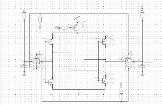
Fig. 4: Schematic Designing of VVc
8T with TG access and Virtual GND/VDD Transistor (VGVc)
Using both TVG and TVV will effectively eliminates any type of short circuit may be present during switching but some other performance criteria will be suffered as we will analyze this latter on. TVG and TVV are controlled by VS signals which are enabled for very short duration. The timing of these signals must be properly maintained.
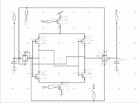
Fig. 5: Schematic Designing of VGVc
RESULTS AND PERFORMANCE ANALYSIS
In this section we have estimated the impact of every proposed SRAM cell on power dissipation and delay for memory overwrite process. All simulation results are carried out for writing ‘1’ when it is assumed that ‘0’is already stored. So node v1 is at GND and v2 at VDD. The circuit is characterized by using 16nm predictive technology which is having a supply voltage of 0.9V.
SIMULATION WAVEFORMS
Waveforms obtained by simulation of proposed SRAM structures on tanner tool clearly depicts timing of each signal and hence the delay performance as shown in Fig 6 of TG SRAM 8T, Fig 7 of VGc, Fig 8 of VVc and Fig 9 of VGVc.
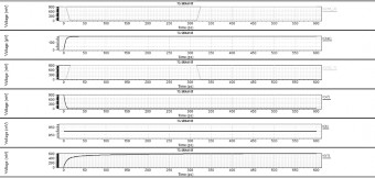
Fig. 6: Waveforms of TG SRAM 8T
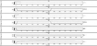
Fig. 7: Waveforms of VGc
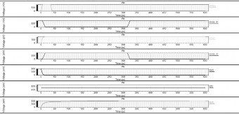
Fig. 8: Waveforms of VVc
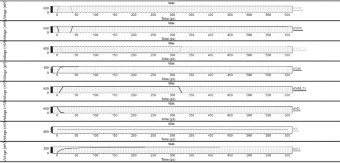
Fig. 9: Waveforms of VGVc
POWER AND DELAY MEASUREMENTS
In each design average dynamic power dissipated through short circuits is measured. Time duration for measuring power is taken by considering the sufficient transition time from on to off state of write enable signal.
while write propagation delay is calculated as the difference in time between when the transitioning W/R signal reaches 50% of VDD and when the latter of the two switching internal nodes (v1 or v2) of the memory cell reaches 50% of VDD.
Power and delay measurements are shown in Table 1
which provides a comparative analysis of all designs.
CONCLUSION
The focus of this paper was to remove the short circuits responsible for significant power losses while writing to memory. For this the addition of virtual source transistor(s) to the standard memory cell was proposed. Delay was intended to be reduced by exchanging the two nMOS access transistors for two CMOS transmission gates. Four different variations of the 6T memory cell were then designed using different combinations of virtual source transistors and transmission gates. Finally, each design was tested through simulation and its performance was evaluated. But most importantly processing with 16nm technology itself is a big advantage which caused shrinking dimensions of the transistor so very small size of memory cell, very low power(<1uw) required for reliable operation of both switching and storage operations, while at the same time also increasing the speed of operation(<10ps) of the device.
TABLE 1: COMPARISON OF POWER AND DELAY IN PROPOSED DESIGNS
S. No | Configuration | Delay ( ps) | Power Dissipa -tion (nw) | Power- Delay Product (nws) |
1. | TG SRAM 8T | 6.82 | 912.02 | 6.22 |
2. | VGc | 6.01 | 766.16 | 4.60 |
3. | VVc | 6.89 | 776.45 | 5.34 |
4. | VGVc | 6.53 | 698.23 | 4.56 |
The most successful design in terms of power consumption and power-delay product is 8T with TG access and Virtual GND/VDD Transistor (VGVc) that is 23.44% and 26.7% less compared to standard 8T SRAM with TG access respectively. However with 11.9% reduction 8T with TG access and Virtual GND Transistor (VGc) is most effective for delay point of view.
As a future scope of this technique and technology it will be
interesting to see if additional transistors used to prevent
dynamic power loss can be used for leakage reduction. Also
we concentrated our power and delay discussion at cell level, so it would be worthwhile to implement any number of the methods for a full system design including cell level, column level and the decoding level.