International Journal of Scientific & Engineering Research Volume 3, Issue 4, April-2012 1
ISSN 2229-5518
Non-Restoring Divider Circuit Using a MCIT Based Adder Cell having Low Energy and High Speed Array
Owk Prasanth Kumar
Abstract--The paper discusses the design of 1-bit full adder circuit using MCIT. This proposed full adder circuit is used as one of the circuit component for implementation of Non- Restoring divider circuits. The proposed adder and divider schematics are designed by using SPICE and their layouts are generated. The divider circuits are designed by using standard NMOS and PMOS 180nm feature size and corresponding power supply 1.8 V. The parameters analyses are carried out by HSPICE analysis. We have compared the simulated results of the Shannon based divider circuit with CMOS adder cell based divider circuits. We have further compared the results with published results and observed that the proposed adder cell based divider circuit dissipates lower power, gives faster response.
Keywords-- CAS, CMOS, Logic gates, MCIT, Multiplexing, Propagation delay, Shannon theorem.
—————————— ——————————
1. INTRODUCTION:
Digital dividers generally can be categorized as employing arithmetic operations to execute a division operation. Arithmetic dividers receive an input that combines the numerator and denominator. Look-up table implementations often require large look-up tables to be accurate for high-speed division, which is generally requiring significant processing time and chip space. Many look-up table implementations also require multiple iterations to improve accuracy, which increases latency associated with the division operation. The processing time required to perform the digital division operation, which corresponds to the amount of time required to perform the division process and referred as latency [1]. In many conventional digital divider designs, the latency determines the overall speed of the division process. As a result, most calculation type dividers typically provide only a few bits of precision for real-time operation.[1]
There are two kinds of array divider such as Non- Restoring Array Divider (NRAD) and Restoring Array Divider (RAD).This paper deals with Non-Restoring and Restoring array divider. The Non-Restoring array divider is guessing the quotient at each stage and when it is wrong it will not correct the remainder in this stage, instead of that it would continue to go to next stage. It has some extra remainder correction circuit after the last stage to correct
the last remainder output by the divider. The Non-
Restoring divider is much more efficient and faster than
regular Restoring array divider. Since the array divider has
many stages, it can be efficiently pipelined. More
importantly, the Non-Restoring divider uses a very regular structure and each cell only needs to connect to the nearest neighbour cells, which makes it very efficient for VLSI design. The Restoring array divider circuit has controlled subtract cell which is used as the cell component of the divider circuit.[1]
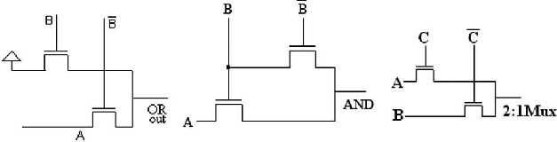
Fig.1:MCIT gates.
IJSER © 2012 http://www.ijser.org
International Journal of Scientific & Engineering Research, Volume 3, Issue 4, March-2012 2
ISSN 2229-5518
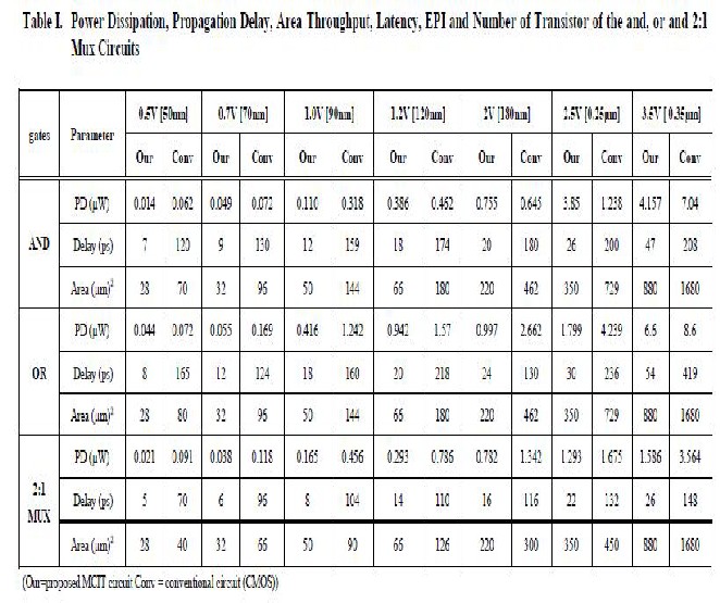
The Fig. (1.1) shows a basic AND, OR and 2:1 Mux circuit, that are designed using by Multiplexing Control Input Technique (MCIT). This logic gate design by MCIT
technique is reduced number of transistor than conventional CMOS circuit. The elaboration of this technique is gives the proposed Shannon full adder cell.
2. ADDER ARCHITECUTE FOR THE ARRAY DIVIDER:
The Shannon Theorem states that any logic expression can be expanded into two terms, the first with a particular variable setting a variable to 1, then multiplying it by the variable and then setting the variable to 0 and multiplying by the inverse. Shannon's Theorem can be stated in a generalized form as:
A function of many variables, f(a 0, a1, a2, ..., ai, ...,
an) can be written as the sum of two terms, one with a
particular variable (say ai) set to 0, and other with it set to 1. f(a0, a1, a2, ..., ai, ..., an) = ai' f(a0, a1, a2, ..., 0, ..., an) + ai f(a0, a1, a2, ..., 1, ..., an) [2]
2.1 ADDER CELL:
The proposed full adder circuit is designed by using Shannon theorem. The full adder sum and carry circuits are designed based on standard adder circuit
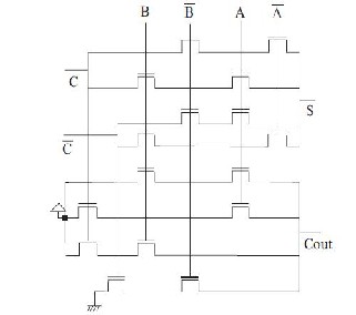
Fig:1.2 CAS cell.
equations . An input B and its complement are used as the control signal of the sum circuit which is shown in Fig. (1.2). The two-input XOR gate is developed using the multiplexer method. The output node of the two-input multiplexer circuit is the differential node. According to standard full adder equation, the sum circuit needs three inputs. In order to avoid increasing the number of
transistors due to the addition of a third input, the following arrangement is made; the CPL XOR gate is multiply with C’s complement input and EXNOR gate is multiplied with input C and this reduces the number of transistors in the sum circuit. Compared with our previous paper, this kind of arrangement cause an increase in the number of transistors but this arrangement avoids the critical path delay. The C and C output node is called the differential node of the circuit . The differential node output is a summing output, as given in Standard full adder equation .[1]
The full adder carry circuit is designed by using fundamental Shannon equation. The source inputs are connected with logic ‘1’, which results always ‘ON’ condition for the transistor. The actual inputs AB, BC and CA are connected in parallel to give the output C=AB+BC+CA. The circuit works according to the standard carry equation. In this circuit, all of the pass inputs are connected at VDD line so that the pass gates are always on. The control input terminals are connected the function inputs.
2.2 SUBTRACTOR CELL:
To find the value (A-B), if assume that the input A is greater than B, we can use only 2’s complement method, which is clearly shown in Fig. (1). In this method, 2’s complement of B is to be added to A and the end around carry is to be ignored. All the bits of B is complemented to get 1’s complement of B and then to the least significant bit B0 is added with ‘1’to get 2’s complement of B. the right most full adder adds A0, B0 and ‘1’. The immediate left full adder circuit adds A1, B1, and C0 and so on. The end carry is ignored. The results A-B is given by DN….D1D0. Signed
2's complement is a modification of the sign-magnitude form in which addition and subtraction of the full adder circuit performed. The high order bit is still the sign bit and logical ‘1’ still indicates a negative number[3]
3. NON-RESTORING DIVISION:
Binary division is basically a procedure to determine how many times the divisor D divides the
IJSER © 2012 http://www.ijser.org
International Journal of Scientific & Engineering Research Volume 3, Issue 4, April-2012 3
ISSN 2229-5518
dividend A thus resulting in the quotient Q . At each step in the process the divisor D either divides A into a group of bits or it does not. The divisor divides a group of bits when the divisor has a value less than or equal to the value of those bits. Therefore, the quotient is either 1 or 0. A basic Non-restoring divider cell consists of a full adder and a XOR gate.[2]
It will read the practical remainder from the previous stage
and depending on the quotient of the last stage it will add the divisor to obtain the remainder for next stage. In this paper the gate level schematic of full adder cells are used to obtain the FET level schematic, which pertains our proposed adder cells. After the design of one cell we can tile them in two dimensions to form a matrix. The Non- restoring array divider cell consists of full adder, and 2 inputs X-OR cells. The divider circuit can be roughly divided into two halves.[3]
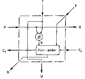
Fig.2: Controlled Adder Subtractor cell (CAS)
Figure 2 shows a single controlled adder-subtractor cell having four inputs T,V,Ci,P and four outputs S,Co,U,Q. The cell function may be summarized as follows: for P = 0, E is the difference and F the borrow generated in forming B- (C+D), while for A = 1, E is the sum and F the carry produced by the addition B+C+D.[2]
4. NON-RESTORING ARRAY DIVIDER:
The design of an array is now described in which subtractions are performed by addition of the divisor in 2's complement form. In the basic cell, shown Fig. 4, a divisor digit presented at the input T is subjected to a controlled complementation, dependent on the state of the control The worst case scenario for the delay was determined to be the one in which all inputs was set to logic high. The speed of the divider circuit can be determined by the
input P, before application to the input R of the full-adder. For P = 0, R = T, while for P = 1, R = T. The full-adder performs the addition V + R + Q to give the sum and carry outputs S and Co. Also, independently of all other inputs, Q = P and U = T. In the Example, a denotes an addition and s a subtraction; sign digits are underlined for identification. The width of the array can be extended to accommodate input data of greater word length, and the number of rows in the array can be increased to give the quotient to as many places as may be required. The operating speed x of the array is given by [2]
T = Ntd + N(N+1)tb + tn
Where td, tb are the signal delays for the sum- difference output E and the carry-borrow output F of a single cell; tn is the delay for a single negating gate. The dividend length, divisor length, quotient length are 2N, N, N+1 respectively.[2]
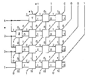
Fig 3 :6X4 divider using CAS cells of fig 2
5. ANALYSIS:
maximum delay along with critical path. A propagation delay of divider circuit for conserving power on a semiconductor chip is provided. The circuit includes a
IJSER © 2012 http://www.ijser.org
International Journal of Scientific & Engineering Research Volume 3, Issue 4, April-2012 4
ISSN 2229-5518
delay chain responsive to a input signal for generating an output signal having a selectively adjustable delay at an output circuit. The delay chain techniques have been developed to reduce the energy dissipation of CMOS design systems. The minimization of power can be carried out by reducing the supply voltage, the capacitance, the number of transitions (e.g. the activity in the circuit) and by optimizing the timing of the signals. A large impact on energy is made by the supply voltage.[1]
By reducing VDD the energy dissipation decreases quadratically but the delay increases and the performance is degraded. A possible solution is that of using different supply voltages the higher voltage. Another technique is to compensate in different parts of the circuit. The parts not in the critical path are supplied by lower voltages, while the critical one by the loss of performance by replicating the hardware (parallelism) to keep the throughput.
5.1 HSPICE CODE:
****CAS****
.subckt cas a2 a21 b b1 c c1 e e1 18 20 15 16
Vd d 0 dc 1.8
*mux
M17 11 e b1 0 nmos l=180nm w=180nm M18 11 e1 b 0 nmos l=180nm w=180nm M19 d 14 12 d pmos l=180nm w=180nm M20 12 14 0 0 nmos l=180nm w=180nm M21 d 11 13 d pmos l=180nm w=180nm M22 13 11 0 0 nmos l=180nm w=180nm M23 d 13 14 d pmos l=180nm w=180nm M24 14 13 0 0 nmos l=180nm w=180nm
*adder
M1 3 a21 c 0 nmos l=180nm w=180nm M2 1 12 3 0 nmos l=180nm w=180nm M3 4 a2 c 0 nmos l=180nm w=180nm M4 1 14 4 0 nmos l=180nm w=180nm M5 5 a21 c1 0 nmos l=180nm w=180nm M6 1 14 5 0 nmos l=180nm w=180nm M7 6 a2 c1 0 nmos l=180nm w=180nm M8 1 12 6 0 nmos l=180nm w=180nm M9 7 a2 d 0 nmos l=180nm w=180nm M10 2 14 7 0 nmos l=180nm w=180nm M11 8 c d 0 nmos l=180nm w=180nm M12 2 14 8 0 nmos l=180nm w=180nm M13 9 c d 0 nmos l=180nm w=180nm M14 2 a2 9 0 nmos l=180nm w=180nm
*output nots
M25 d 1 15 d pmos l=180nm w=180nm M26 15 1 0 0 nmos l=180nm w=180nm M27 d 2 16 d pmos l=180nm w=180nm M28 16 2 0 0 nmos l=180nm w=180nm M29 d 1 17 d pmos l=180nm w=180nm M30 17 1 0 0 nmos l=180nm w=180nm M31 d 17 18 d pmos l=180nm w=180nm M32 18 17 0 0 nmos l=180nm w=180nm
M33 d 2 19 d pmos l=180nm w=180nm M34 19 2 0 0 nmos l=180nm w=180nm M35 d 19 20 d pmos l=180nm w=180nm M36 20 19 0 0 nmos l=180nm w=180nm
.ends cas
Va0 a0 0 0
Va01 a01 0 1.8
Va1 a1 0 0
Va11 a11 0 1.8
Va2 a2 0 0
Va21 a21 0 1.8
Va3 a3 0 0
Va31 a31 1.8
Va4 a4 0 1.8
Va41 a41 0 0
Va5 a5 0 0
Va51 a51 0 1.8
Vb b 0 0
Vb1 b1 0 1.8
Vb11 b11 0 1.8
Vb111 b111 0 0
Vb0 b0 0 0
Vb01 b01 1.8
Ve e 0 1.8
Ve1 e1 0 0
X1 a2 a21 b b1 e e1 e e1 18 20 15 16 cas
X2 a1 a11 b11 b111 20 16 e e1 l k l1 k1 cas
X3 a0 a01 b0 b01 k k1 e e1 m q0 m1 q01 cas X4 a3 a31 b b1 q0 q01 q0 q01 o p o1 p1 cas X5 18 15 b11 b111 p p1 q0 q01 r s r1 s1 cas X6 l l1 b0 b01 s s1 q0 q01 t u t1 u1 cas
X7 m m1 e1 e u u1 q0 q01 v q1 v1 q11 cas X8 a4 a41 b b1 q1 q11 q1 q11 w x w1 x1 cas X9 o o1 b11 b111 x x1 q1 q11 y z y1 z1 cas X10 r r1 b0 b01 z z1 q1 q11 f g f1 g1 cas
X11 t t1 e1 e g g1 q1 q11 h q2 h1 q21 cas
IJSER © 2012 http://www.ijser.org
International Journal of Scientific & Engineering Research Volume 3, Issue 4, April-2012 5
ISSN 2229-5518
X12 a5 a51 b b1 q2 q21 q2 q21 i j i1 j1 cas
X13 w w1 b11 b111 j j1 q2 q21 s13 c13 s131 c131 cas X14 y y1 b0 b01 c13 c131 q2 q21 s14 c14 s141 c141 cas X15 f f1 e1 e c14 c141 q2 q21 s15 q3 s151 q31 cas
.tran 1 200 10
***180nm CMOS model files included from
http://ptm.asu.edu/
.end
5.2 CODE ANALYSIS:
The code is written for the Fig:1 for each CAS cell and calling it for the other CAS cells in the matrix of Fig:3 .The main advantage of this code is the use of PMOS and NMOS and adding CMOS buffers near the output, thereby getting the outputs similar and accurate to the outputs of the general CMOS gates with a lesser number of gates thereby decreasing the propagation delay of the cell and hence the circuit. The Vcc is given a rudimentary voltage of 1.8 volts for simulation purposes.
The numbers from 1 to 36 represent the different nodes,
the code is divided into different parts like the MUX
represented in the fig 1.2 the output nodes being the buffers at the outputs of the divisor and the remainder for the 6X4 matrix shown in fig.3.Further the adder subpart of the code represents the basic CAS cell which is used for the other 23 cells. The transient analysis of the output is observed and verified for all the 6 bit dividend and 4 bit non-zero divisor. The model files should be included in the code at the location shown. This code can be made to work for any CMOS technology by including the required model files. Minimum amount of glitches are observed during the transitions.
IJSER © 2012 http://www.ijser.org
International Journal of Scientific & Engineering Research Volume 3, Issue 4, April-2012 6
ISSN 2229-5518
IJSER © 2012 http://www.ijser.org
lnt<!mational Journal of Scientific & Engineering Research Volwne 3, Issue 4, April-2012 7
JSSN 2229-5518
Table 2. Comparison of Power Dissipation, Propagation Delay and Area for 1-bit Adder Cell Designed 1 th Different Technique
Addtl' Type | Supply \'oltage | .5\' [50nm[ | 0.7\' [70nm] | !.0\' [90nm] | 1.2\' !l!Onm] | 2\' USOnm] | 2.5\' [0.25IIID] | 3.5Y [0.351tm] | 5\'[0.6111D] |
ShaJUJon | Power fl\V | 0.042 | 0.371 | 0.442 | 0.569 | 1.984 | 12.64 | 24.88 | 58.6 |
ShaJUJon | Delay (ps) | 2 | 4 | 6 | 13 | 23 | 29 | 54 | 114 |
ShaJUJon | Areaijtm | 15x7 | 22xl0 | 23xll | 28x14 | 37x26 | 62x32 | 84x52 | 142x80 |
Mi.\ed ShaJUJon [13] | Power\V | 0.309 | 0.437 | o.m | 0.658 | 2.529 | 14.8 | 31.13 | 84.05 |
Mi.\ed ShaJUJon [13] | Delay (ps) | 6 | 12 | 18 | 22 | 25 | 49 | 70 | 105 |
Mi.\ed ShaJUJon [13] | Area(flill | 16x7 | 16x9 | 17x10 | 20x9 | 19x12 | 52x30 | 82x48 | 124x74 |
CPL | Power fl\V | 0817 | 2.247 | 3.249 | 4.907 | 9.936 | 14.782 | 29.69 | 48.75 |
CPL | Delay (ps) | 14 | 23 | 31 | 81 | 87 | 205 | 324 | 640 |
CPL | Area(flill | HxS | 19x10 | 20x12 | 24x14 | 49x28 | 62x35 | 9Sx56 | 148x86 |
CMOS | PowerftW | 1.49 | 3.76 | 7.06 | 10.69 | 14.04 | 25.l4 | 29.10 | 32.25 |
CMOS | Delay (ps) | 654 | 854 | 971 | 995 | 1000 | 1401 | 1602 | 1995 |
CMOS | Areaijtm | 15x7 | 53xl0 | 67x14 | 74xll | 93x26 | 117>:32 | 186x52 | 280x80 |
IJSER ®2012
hno:Hwww jjser.oro
International Journal of Scientific & Engineering Research Volume 3, Issue 4, April-2012 8
ISSN 2229-5518
**The table sources are from Low Energy, Low Latency and High Speed Array Divider Circuit Using a Shannon Theorem Based
Adder Cell by Chinnaiyan Senthilpari, Krishnamoorthy Diwakar and Ajay K. Singh.
6. CONCLUSION:
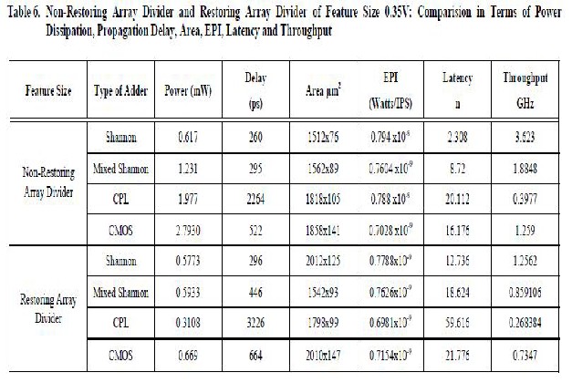
Our proposed MCIT adder cell consists of 16 transistors and mixed Shannon based adder cell consists of 12 transistors compare to CPL-18 transistor and CMOS -28 transistors. The Non Restoring 6x4 bit divider circuits are simulated by using HSPICE TOOL. All the outputs checked from 1111111 ÷ 0001 to 111111 ÷ 1111. Various parameters such as area, propagation delay, dissipated power, throughput, latency and EPI are determined from array dividers layout of feature size 180nm. The divider circuits are analyzed using BSIM 4 parameter analyzer and results are given in Table 6. Our proposed Shannon adder based Non-Restoring array divider circuit gives less power dissipation, lower delay, low EPI, low latency and high throughput compared with mixed Shannon, CPL and CMOS based array divider circuits due to
lower critical path in our proposed adder cell[1]. Similarly,
dominance reflects in the restoring array divider circuit in
terms of power, delay, EPI, latency and throughput. Our MCIT based Non-restoring array divider circuit shows an improvement of 12.16% in propagation delay, 2% in EPI,
81.87% in latency and 65.32% in throughput compared to Shannon based Restoring array divider circuit. [1]The Non- restoring divider circuit implemented by using our proposed MCIT based adder cell dissipates lower power than CPL, CMOS and mixed Shannon based adder cell divider circuits irrespective of power supply . [1]
The design has been presented for the non- restoring division in fig.3. Equations for the operating speeds of this array indicate that the logical design of the cells should be primarily achieve the rapid propagation of signals along the rows.
The following are the advantages:
1. Quotient digits are obtained from cell outputs without the use of extraneous gates.
2. The use of carry signal for control, rather than as a sum signal enhances the operating speed.
3. Use of CMOS buffers at only the outputs and PMOS and
NMOS everywhere else reduces the number of logic gates required.
4. The fan out of the circuit drastically increase compared to the CPL circuits.
IJSER © 2012 http://www.ijser.org
International Journal of Scientific & Engineering Research Volume 3, Issue 4, April-2012 9
ISSN 2229-5518
5. The array can be implemented using small number of transistors.
6. Finally as the number of gates decreases, even the propagation delay decreases hence increasing the speed of computation.
7. REFERENCES:
1. “Low Energy, Low Latency and High Speed
Array Divider Circuit Using a
Shannon Theorem Based Adder Cell” Chinnaiyan Senthilpari, Krishnamoorthy Diwakar and Ajay K. Singh- Recent Patents In Nano Technology, 2009 .
2. H.H.Guild-“Some cellular logic arrays for non-restoring division”.(The Radio and Electronic Engineer,Vol 39,1970.)
3. “An augumented iterative array for high speed binary division”
Marus Cappa and V.Carl Hamacher
IEEE Transactions of computers,Vol- c22,no:2, ,1973
Owk Prasanth Kumar is from Visakhapatnam, Andhra Pradesh and pursuing his 3rd Year of Bachelor degree(2009-13) in Electronics and Communication Engineering from Visvesvaraya National Institute of Technology(VNIT), Nagpur, Maharashtra ,India. owkprasanthkumar@ece.vnit.ac.in
prashanth.bobby183@gmail.com
IJSER © 2012 http://www.ijser.org