International Journal of Scientific & Engineering Research, Volume 5, Issue 3, March-2014 1200
ISSN 2229-5518
Metal based Synthesis of Graphene by Pulsed
Laser Deposition Technique
Umber Kalsoom*, M. Shahid Rafique, Rabia Shaheen, Khizra Fatima.
Abstract— Pulsed laser deposition technique was used to investigate the effect of cobalt and silver on the fabrication of graphene layers on silicon substrate at 500oC temperature. A uniform and layer by layer deposition of the graphene film has been identified by Atomic Force Microscopy. Micro Raman spectroscopy revealed that by increasing graphite content there is decrease in I D /I G ratio and increase in I 2D /I G ratio which is indicative of the formation of low defect, monolayer and few layer graphene.
Index Terms— Graphene, Pulsed Laser Deposition, Raman Spectroscopy, Atomic force Microscopy.
—————————— ——————————
Graphene is a flat, 2D monolayer of sp2 hybridized carbon atoms tightly packed in closed hexagonal crystal structure [1]. In regular hexagon graphene layer C-C bond length is
0.142nm while interplanar spacing is of the order of 0.335 nm [2]. Graphene can be wrapped up into 0D fullerene C60 , rolled into 1D nanotube CNT and also stacked into 3D graphite (C) [1].
In microelectronics, graphene is proved to be a good replacement of silicon due to its strong bonding and unique electronic, thermal and mechanical properties [2]. All these inspiring and attractive graphene’s properties need high availability of controllable and reliable fabrication techniques. In literature, mono and few-layer graphene has been fabricated by many methods such as micromechanical cleavage (drawing) method [3], thermal decomposition and metal induced graphitization [4,5], graphite oxide reduction [6], molecular beam epitaxy (MBE) [7], chemical vapor deposition (CVD) [8] and the most recently by pulsed laser deposition (PLD) technique [9,10].
Carbon deposition on metal has been gaining attention as an alternative graphene fabrication method. Growing interest of graphene formation on metal occur due to its reduced temperature, less rigorous vacuum conditions and easily transferring of graphene to other arbitrary substrates by dissolving the metal layer [11]. This paper describes the fabrication of few-layer graphene by PLD technique at 500oC substrate temperature.
A limited amount of carbon was deposited on cobalt (Co) and silver (Ag) thin films at 500oC substrate temperature by pulsed laser ablation of graphite. High energetic carbon species form a solid solution of C-Co or C-Ag into the Co and Ag metals used respectively.
Author to whom correspondence should be addressed. Electronic mail: umber@uet.edu.pk. Tel.: +92 42 99029204.
a crystalline hexagonal carbon layer appears at the top surface. In this comparative study, effect of Co and Ag metals on the quality of graphene was discussed.
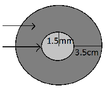
In this experiment few-layer graphene has been deposited by using cobalt-graphite (Co-C) and silver-graphite (Ag-C) targets on n+ silicon (100) substrate. Cobalt and silver were used as catalyst. Co-C and Ag-C has been prepared by embedding cobalt disc into the graphite disc and after Co-C deposition, cobalt was replaced by silver in the same graphite disc. Schematic of targets Co-C and Ag-C is shown in Fig. 1. Targets were mounted on motorized target holder placed in stainless steel chamber which was evacuated to a pressure of
10-5 torr. A KrF excimer laser (248 nm, 20 mJ, 20 Hz) was focused at an angle of 45˚ on targets Co-C and Ag-C. Silicon is placed in parallel configuration with targets at a distance of
2cm. Schematic of the experiment is shown in Fig. 2.
Experiment was done in two steps. In 1st step, chamber
was evacuated with base pressure of the order of 10-5 torr in
three hours. After that 5000 shots from KrF excimer laser (248
nm, 20 mJ, 20 Hz) were given to cobalt (Co), ablated material
was deposited on silicon substrate. Then substrate (Si)
temperature was raised to 500 ºC for 1 hour and metal
particles arrange uniformly to provide matrix for carbon
atoms. In 2nd step, after heating substrate to 500 ˚C, graphite
came in front of KrF excimer laser by using electric stepper
motor. 200 laser shots were given to graphite and the ablated
graphite particles were deposited on heated Co-Si substrate.
Finally, carbon was precipitated out from metal-carbon solid
solution on natural cooling upto room temperature and
adsorbed energetic carbon atoms form crystalline hexagonal
structure which leads to the formation of few-layer graphene.
1st step and 2nd step were repeated by giving 5000 shots to
cobalt and 500 shots to graphite respectively. Same procedure
was adopted by taking silver as a catalyst and graphite as
carbon source.
During natural cooling of deposited films till room temperature, carbon precipitated out from solid solutions and
IJSER © 2014 http://www.ijser.org
International Journal of Scientific & Engineering Research, Volume 5, Issue 3, March-2014 1201
ISSN 2229-5518
Fig. 1. Schematic of Co-C and Ag-C target assembly
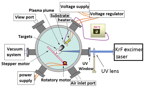
Fig. 2. Schematic of experimental setup
These fabricated films were then analysed by Raman spectroscopy for structural analysis while surface topography of deposited films were explored by Aomic Force Microscopy (AFM).
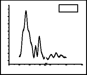
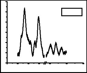
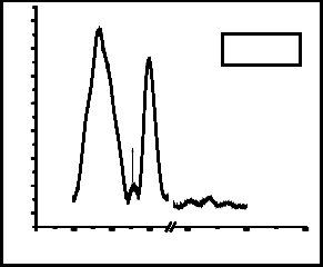
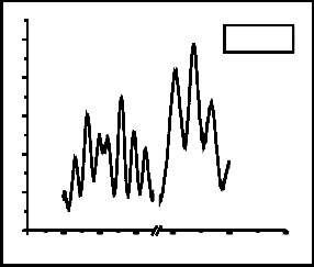
Fig. 3 shows the spectra of Raman analysis of films grown with (a) Co: 5000 shots, C: 200 shots, (b) Co: 5000, C: 500 shots, (c) Ag: 5000 shots, C: 200 shots and (d) Ag: 5000
shots, C: 500 shots. All the Raman spectra show three common prominent graphene peaks. These are D peak, G peak and 2D peak which occurs at ~1330 cm-1, ~1588 cm-1 and ~2670 cm-1. D-band mostly appears due to asymmetric breathing mode of sp2 carbon structure [12]. The D and 2D peaks are due to double resonant scattering processes [13]. The D peak is absent in perfectly crystalline graphene. G peak measures the degree of graphitization, it is non- dispersive and occurs due to in-plane bond stretching of sp2 hybridized carbon atoms [12].
In all Raman spectra, there appears a side peak with G peak at ~1519cm-1. This is SiC peak which occurs due to the direct interaction of carbon particles with silicon substrate. The occurrence of 2D peak confirms the formation of graphene.
IJSER © 2014 http://www.ijser.org
International Journal of Scientific & Engineering Research, Volume 5, Issue 3, March-2014 1202
ISSN 2229-5518
G
Co:5000 shots
C : 200 shots
2D Co:5000 shots
C:500 shots
SiC
SiC D
Co G
2D
1000 1200 1400 1600 2600 2800 3000
Wave number (cm-1)
1000 1200 1400 1600 2600 2800 3000
Wave number (cm-1)
Ag:5000 shots
C:200 shots
G
Ag:5000 shots
C:500 shots
G
SiC
2D
SiC 2D
1000 1200 1400 1600 2600 2800 3000
Wave number (cm-1)
1000 1200 1400 1600 2600 2800 3000
Wave number (cm-1)
Fig. 3: Raman analysis of films grown with (a) Co: 5000 shots, C: 200 shots, (b) Co: 5000, C: 500 shots, (c) Ag: 5000 shots, C: 200 shots and (d) Ag: 5000 shots, C: 500 shots.
However, the shape and intensity of 2D peak describes the number of graphene layers or graphene thickness. For monolayer graphene, 2D band has single symmetric peak while in bi-layer 2D peak splits into 4 peaks. Splitting occurs due to four double resonance scattering processes. For the case of monolayer graphene there is only one double resonance scattering process. As the number of layers increases, the number of doubly resonance processes also increases and the shape moves towards graphite spectra [14]. As such, looking at Raman spectra it can be seen that monolayer and few-layer graphene has been fabricated. Table I shows Raman data analysis of monolayer and few ayer graphene growth on cobalt and silver metals with different graphite shots at 500 ˚C substrate temperature. From Raman data of films grown with C: 200 and C: 500 shots on metals, I D /I G ratio indicates disorder and defects. These defects are produced due to
clustering of carbon atom upon cooling. As carbon concentration on catalyst cobalt increases there is a decrease in I D /I G ratio which shows that less defects are produced. It is observed that I D /I G ratio decreases on increasing carbon concentration which depicts phase transition in structure from non-sp2 to sp2 bonding. Hence, less defects and more crystalline graphene layers are produced by taking graphite
500 shots on metals.
Intensity ratio of 2D and G band (I 2D /I G ) is sensitive to
number of graphene layers. I 2D /I G for film with Co: 5000
shots and C: 200 shots is 0.115 [9] which translates to the
formation of few-layer graphene (< 10 layers) while I 2D /I G
ratio for the film grown at Co: 5000 shots and C: 500 shots is
1.890 [15] which confirms the formation of monolayer
graphene. For monolayer graphene 2D-peak intensity
should be double than that of G-peak intensity i.e. I 2D /I G ≈ 2
[9].
IJSER © 2014 http://www.ijser.org
International Journal of Scientific & Engineering Research, Volume 5, Issue 3, March-2014 1203
ISSN 2229-5518
Table I. Raman analysis data of monolayer and few-layer
graphene.![]()
![]()
No. of laser shots Intensity ratio
Metals Graphite ID / IG I2D /IG
For as-grown films with Ag: 5000 shots and C: 200 shots I 2D-
/I G ratio is 0.343. This value indicates the formation of < 5
layers graphene. Film with Ag: 5000 shots and C: 500 shots
show I 2D /I G ratio is 0.446 which translates to the formation
Cobalt | 5000 | 200 | 1.187 | 0.115 | of few-layer graphene (< 5 layers) [16]. Raman analysis confirms the formation of few-layer |
Co | 5000 | 500 | 1.17 | 1.890 | graphene on both cobalt and silver transition metals at 500 |
Silver | 5000 | 200 | 2.07 | 0.343 | ˚C substrate temperature by PLD. However, cobalt as a |
Ag | 5000 | 500 | 1.183 | 0.446 | catalyst facilitates monolayer graphene synthesis with less |
structural defects as compared to that of silver catalyst. |
![]()
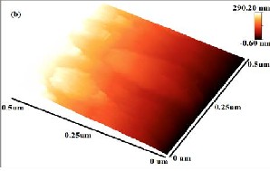
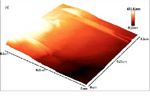
The topography of monolayer and few-layer graphene grown by pulsed laser deposition is characterized by using AFM (Veeco) operated in non-contact mode. 3D AFM
image of films grown at (a) Co: 5000 shots and C: 200 shots, (b) Co: 5000 shots and C: 500 shots, (c) Ag: 5000 shots and C: 200 shots and (d) Ag: 5000 shots and C: 500 shots is
Cobalt: 5000 shots and graphite: 200 shots Cobalt: 5000 shots and graphite: 500 shots
Silver: 5000 shots and graphite: 200 shots Silver: 5000 shots and graphite: 500 shots
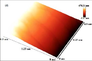
Fig. 4: AFM analysis of film grown at (a) Co: 5000 shots and C: 200 shots, (b) Co: 5000 shots and C: 500 shots, (c) Ag: 5000 shots and C: 200 shots, (d) Ag: 5000 shots and C: 500 shots.
shown in Fig. 4. Fig. 4(a, b, d) shows different layered patterns which can be distinguished from color contrast bar given in AFM images. Black region in the 3D image is the reference silicon surface. Red region corresponds to metal
deposition at 500˚C while light yellow color indicates carbon particles segregation on metal which results in monolayer Fig. 4(b) and few-layer Fig. 4(a, d) graphene formation. Total thickness of deposited films in Fig. 4(a, b,
IJSER © 2014 http://www.ijser.org
International Journal of Scientific & Engineering Research, Volume 5, Issue 3, March-2014 1204
ISSN 2229-5518
d) is 678, 291 and 695nm respectively. In Fig. 4(c) film prepared with silver and low carbon concentration (200 laser shots) shows some aggregates of carbon atoms immersed in catalyst. Surface patterns shows nucleation which results in the formation of discrete metal islands which grow with low carbon species absorption and finally converged to form few-layer graphene film. This shows that the solubility limit decreases at low concentration of carbon particles on metals as insufficient carbon atoms accumulate on metal surface and forms few-layer graphene (Fig. 4(a, c)). However, by increasing carbon concentration at 500˚C on cobalt and silver, the solubility of carbon in metals increases which results in the formation of uniform
monolayer graphene and few-layer graphene. In comparison, carbon films grown on cobalt has more uniform layered patterns with fewer defects as compared to carbon films grown on silver catalyst.
Formation of few-layer graphene on transition metals cobalt and silver was investigated. By increasing graphite content on cobalt and silver, low-defect few-layer and monolayer graphene can be successfully obtained at 500˚C substrate temperature. However, cobalt as a catalyst facilitates monolayer graphene synthesis with less structural defects as compared to that of silver as catalyst.
[1] A. K. Geim, and K. S. Novoselov, “The Rise of
Graphene” Nature Materials 6(3), pp. 183-191, 2007.
[2] D. R. Dreyer, R. S. Ruoff and C. W. Bielawski, “From
Conception to Realization: An Historic Account of
Graphene and Some Perspectives for its Future”,
Angewandte Chemie International 49, pp. 9336-9344, 2010.
[3] K. S. Novoselov, A. K. Geim, S. V. Morozov, D. Jiang, Y.
Zhang, S. V. Dubonos, I. V. Grigorieva and A. A. Firsov,
“Electric Field Effect in Atomically Thin Carbon Films”,
Science 306, pp. 666-669, 2004.![]()
[4] S. Y. Cho, H. M. Kim, M. H. Lee, D. J. Lee, K. B. Kim,
Current Applied Physics 12 (4), pp. 1088–1091 2012.![]()
[5] R. S. Edwards and K. S. Coleman, Acc. Chem.
Res. 46 (1), pp. 23–30 2013.
[6] S. Stankovich, D. A. Dikin, R. D. Piner, K. A. Kohlhaas,
A. Kleinhammes, Y. Jia, et al Carbon 45, pp. 1558–1565 2007.
[7] E. Moreau, F. J. Ferrer, D. Vignaud, S. Godey and X.
Wallart, “Graphene Growth by Molecular Beam Epitaxy
Using a Solid Carbon Source”, Physica Status Solids 207(2),
pp. 300-303 2010.
[8] A. Reina, X. Jia, J. Ho, D. Nezich, H. Son, V. Bulovic, M.
S. Dresselhaus and J. Kong, “Layer Area, Few-Layer
Graphene Films on Arbitrary Substrates by Chemical Vapor
Deposition”, Nano Lett. 9(1), pp. 30-35 2009.
[9] K. Wang, G. Tai, K. H. Hong, S. P. Lau, and W. Guo, “Ni
Induced Few-Layer Graphene Growth at Low Temperature
by Pulsed Laser Deposition”, American Institute of physics
1, pp. 022141-9 2011.
[10] A. T. T. Koh, Y. M. Foong and D. H. C. Chua,
“Comparison of the Mechanism of Low Defect Few-Layer
Graphene Fabrication on Different Metals by Pulsed Laser
Deposition”, Diamond and Related Materials 25, pp. 98-102
2012.
[11] C. He, W. Wang, S. Deng, N. Xu, Z. Li, G. Chen and J.
Peng, J. Phys. Chem. A 113 pp. 7048–7053 2009.
[12] A. C. Ferrari and J. Robertson, “Interpretation of![]()
Raman Spectra of Disordered and Amorphous Carbon”,![]()
Physical Review B (Condensed Matter and Materials
Physics) 61(20), pp. 14095-14107 2000.![]()
[13] A. N. Obraztsov, E. A. Obraztsova, A. A. Zolotukhin
and A. V. Tyurnina, Journal of Experimental and
Theoretical Physics, 106 (3), pp. 569–574 2008.
[14] A. C. Ferrari, J. C. Meyer, V. Scardaci, C. Casiraghi, M.
Lazzeri, F. Mauri, S. et al Phys. Rev. Lett. 97(18), pp. 187401-
4 2006.
[15] D. Graf, F. Molitor, K. Ensslin, C. Stampfer, A. Jungen,
C. Hierold, et al Nano Lett. 7, 238, 2007.
[16] A. T. T. Koh, Y. M. Foong, and D. H. C. Chua, “Cooling
Rate and Energy Dependence of Pulsed Laser Fabricated
Graphene on Nickel at Reduced Temperature”, Appl. Phys.
Lett. 97, pp. 114102-3 2010.
IJSER © 2014 http://www.ijser.org