International Journal of Scientific & Engineering Research Volume 2, Issue 6, June-2011 1
ISSN 2229-5518
Low-Power 1-bit CMOS Full Adder Using
Subthreshold Conduction Region
Vishal Sharma, Sanjay Kumar
Abstract— In balancing the trade-off between power, area and performance, numerous efforts have been done. However, not much study has been done at the two extreme ends of the design spectrum, namely the ultra low-power with acceptable performance at one end (the main concern of this paper), and high performance with power within limit at the other. This paper is based on the exclusive use of subthreshold conduction currents to perform circuit operations, yielding a dramatic improvement in power consumption compared to traditional circuit design approaches. This improvement makes it feasible to design extreme low-power circuits with such an approach. The CMOS digital circuits for this work have been designed using standard TSMC 0.18 Jlm Technology.
Index Terms— Low-Power, Subthreshold Conduction Region, Full Adder.
.
—————————— • ——————————
N most VLSI applications, arithmetic operations play an important role. Commonly used operations are addition, subtraction, multiplication and accumulation, and 1-bit Full Adder is the building block for most implementations of these operations. Obviously, enhancing the building block performance is critical for enhancing overall system performance [1] and in present, the power consumption has become a critical concern in today’s VLSI system design. The need for low-power VLSI systems arises from two main forces. First, with the steady growth of processing capacity per chip, large current has to be delivered and the heat due to large power consumption must be removed by proper cooling techniques. Second, battery life in portable electronic devices is limited. Low-power design directly leads to
prolonged operation time in these portable devices [2].
Subthreshold circuit design provides an efficient solution to significantly reduce the power. So this work is based on subthreshold conduction principle to design a low-power 1-bit Full Adder. In subthreshold circuits, the supply voltage is reduced well below the threshold voltage of a transistor. Due to the quadratic reduction in power with respect to the supply voltage, subthreshold circuits are classified as ultra low-power circuits.
Specifically in application areas where performance
can be sacrificed for low-power, subthreshold circuits are an ideal fit. Some of the applications include devices such
————————————————
• Sanjay Kumar is currently working as Assistant Professor in Electronics
and Communication Engineering Department in Thapar University,
Patiala, Punjab, India. E-mail: sanjay.kumar@thapar.edu
as digital wrist watches, radio frequency identification (RFID), sensor nodes, pacemakers and battery operated devices such as, cellular phones [3].
Up until now, the power consumption has not been of great concern because of the availability of large packages and other cooling techniques having the capability of dissipating the generated heat. However, continuously increasing density as well as the size of the chips and systems might cause to difficulty in providing adequate cooling and hence, might either add significant cost to the system or provide a limit on the amount of the functionality that can be provided [4].
Another factor that fuels the need for low-power chips is the increased market demand for portable consumer electronics powered by batteries. For these high performance portable digital systems, running on batteries such as-laptops, cellular phones and personal digital assistants (PDAs), low-power consumption is a prime concern because it directly affects the performance by having effects on battery longevity.
Hence, low-power 1-bit Full Adder design has assumed great importance as an active and rapidly developing application in VLSI. Due to their extreme low- power consumption, subthrehsold design approaches are appealing for a widening class of applications which demand low-power consumption and can tolerate larger circuit delays.
IJSER © 2011 http://www.ijser.org
International Journal of Scientific & Engineering Research Volume 2, Issue 6, June-2011 2
ISSN 2229-5518
Digital subthreshold circuits are currently used for some low-power applications such as hearing aids, wrist
Equation (2) shows the same basic equation with low
Vds roll-off:
watches, pacemaker and wireless communication systems
Vgs-Vth
-Vds
[5]. In subthreshold circuit design, supply voltage must![]()
Ion-sub = I0 exp
![]()
1- exp (2)
nVT VT
be scaled down below the threshold voltage. Therefore, the load capacitance is charged or discharged by the
where I0 is the drain current when Vgs = Vth given below:
subthreshold leakage current. When the Adder circuits
operate in the subthreshold region, they should have
w
0 eff ox Leff
(n - 1)VT
(3)
different performance characteristics than those of the Adders working in the strong inversion region [6]. In this paper, we will see the characteristics of a 1-bit Full Adder cell operating in subthreshold region of operation
As expected for the diffusion current, (1) shows that
Ion–sub depends exponentially on Vgs . Here, W is the width of the transistor, Leff is the effective length, µeff is the effective mobility, Cox is the oxide capacitance, n is the
comparing it with the 1-bit Full Adder cell operating in![]()
subthreshold slope factor n = 1+ , Vth
is the
strong inversion.
In traditional digital VLSI design, subthreshold region of operation is avoided, since it contributes toward leakage power consumption when the device is in stand- by. But the power can be reduced significantly by exclusively utilizing this subthreshold leakage current to implement circuits. This is achieved by actually setting
the circuit power supply Vdd to a value less than or equal
to Vth . The subthreshold current is exponentially related
to gate voltage giving the exponential reduction in power
consumption, but also an increase in circuit delay [7]. So, we use the circuits operating in subthreshold conduction region where the power is main concern and large delay can be tolerated.
cox
transistor threshold voltage and VT is the thermal voltage,
VT = (kTjq).
In this section, we will discuss a closed form solution
for the optimum Vdd and Vth for a given frequency and
technology operating in the subthreshold region means
(Vdd Vth).
The total energy per operation of a digital CMOS
circuit consists of two components: switching and leakage energy [9]. Here, we discuss in terms of an inverter.
Hence, total energy per operation can be expressed as:
ETotal = ESw + EL
2 -Vdd
![]()
= Vdd Ceff + Weff KCg LDP exp nV
(4)
where, Ceff is the average effective switched capacitance per operation, K is a delay fitting parameter, Cg is the output capacitance of the inverter and LDP is the depth of
the critical path.
By using (1), (2), (3) and (4), the equations for optimum
supply voltage Vdd,opt and optimum threshold voltage
Vth,opt can be derived as shown in (5) and (6) respectively
[3].
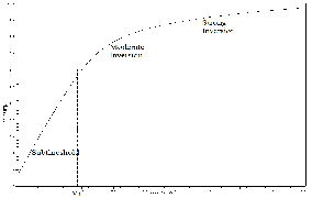
Fig. 1 CMOS Conduction region for an NMOS with Vds = 1.8 V and
Vgs varying from 0 V to 1.8 V.
Vdd,opt = nVT 2– lambert W
![]()
-2ceff
weff cgL
exp(2) (5)
Unlike moderate and strong inversion, in which the drift component of current dominates, subthreshold
conduction is dominated by diffusion current [8].
Also, we can find the optimum value of Vth = Vth,opt
for a given frequency f as:![]()
f cg L Vdd,opt
Vth,opt = Vdd,opt - nVT loge I
(6)
In subthreshold conduction, the channel of the transistors is not inverted and current flows by diffusion. Subthreshold current can be expressed by the following basic equation:
Vgs-Vth
If the argument to the natural log in (6) exceeds 1, then the assumption of subthreshold operation no longer holds
because Vth,opt Vdd,opt . This constraint shows that there is
a maximum achievable frequency for a given circuit in
the subthreshold region [9].![]()
Ion–sub = I0 exp
nVT
(1)
Swanson and Meindl analysed the VTC of an inverter
IJSER © 2011 http://www.ijser.org
International Journal of Scientific & Engineering Research Volume 2, Issue 6, June-2011 3
ISSN 2229-5518
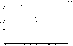
and showed that the inverter operation could be simulated down to 100 mV [10]. The VTC curves for different supply voltages for an inverter are shown in Fig.
2. To find the minimum voltage, Swanson equated the off
current of NMOS and PMOS and calculated the inverter gain in subthreshold. Since an inverter must have
sufficient gain at Vdd /2, the minimum voltage to be used
was estimated to be 8(kT/q) or 0.2 V [10].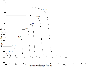
Fig. 2 Inverter VTC showing operation down to 100 mV in a 0.18 µm process.
This section describes the design of 1-bit CMOS Full Adder operating in subthreshold conduction region. Before this design, the basic CMOS Inverter, shown in Fig. 3, is analysed in detail and then, based on this analysis, 1-bit Full Adder can be designed by calculating the values of W/L with the help of these W/L values of Inverter which has been designed for symmetric output and equal charging and discharging current.
Fig. 3 Basic CMOS Inverter
By simulating this CMOS Inverter using TSMC 0.18 µm
technology, the Inverter’s values of W/L for PMOS = (1.2
µm/0.18 µm) and W/L for NMOS = (0.27 µm/0.18 µm) were
obtained for strong inversion operation. While the Inverter’s values of W/L for PMOS = (3.0 µm /0.18 µm) and W/L for NMOS = (0.27 µm/0.18 µm) were obtained for subthreshold operation.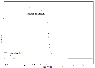
Fig. 4 VTC curves for Inverters operating in strong inversion and subthreshold.
Using these values of W/L of basic Inverter, Full Adder circuit can be designed having the equivalent W/L values equal to that of this basic Inverter [3].
The load capacitance, for the inverter described in previous section, for strong inversion region is 5 fF while the load capacitance for subthreshold conduction is 11 fF.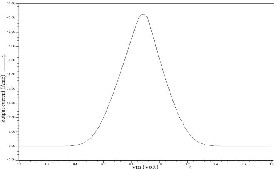
Fig. 5 Output current variation with input voltage in strong inversion
region with Vdd = 1.8 V.
From Fig. 5 and 6, it is clear that the current depends
on input (gate) voltage linearly in strong inversion region and exponentially in subthreshold region.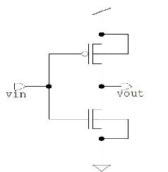
IJSER © 2011 http://www.ijser.org
International Journal of Scientific & Engineering Research Volume 2, Issue 6, June-2011 4
ISSN 2229-5518
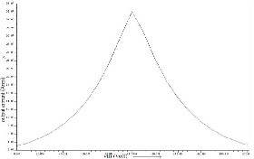
Fig. 6 Output current variation with input voltage in subthreshold
region with Vdd = 0.2 V.
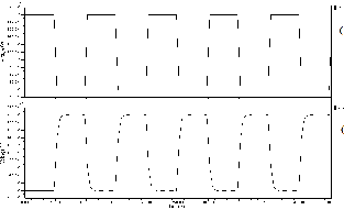
Fig. 7 Simulation result of transient analysis for CMOS Inverter in subthreshold region: (a) Input Signal, (b) Voltage waveform of Output Signal.
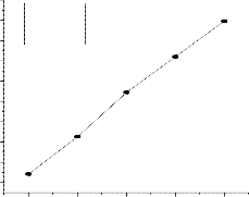
Fig. 8 shows the dynamic power variation with different clock frequencies for a 1-bit Full Adder operating in subthreshold conduction region.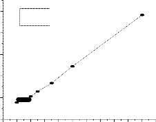
0.010 V = 0.2 V
dd
The basic structure and simulation result for a 1-Bit
CMOS Full Adder are shown in figures given below.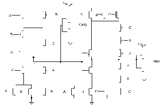
Fig. 9 Basic Structure of a 1-Bit CMOS Full Adder.
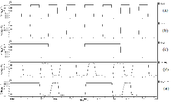
Fig. 10 Simulation result of transient analysis for a 1-Bit CMOS Full Adder in subthreshold conduction region: (a) Input Signal (A), (b) Input Signal (B), (c) Input Signal (C), (d) Voltage waveform of Output (SUM) Signal, (e) Voltage waveform of Output (CARRY) Signal.
TABLE I
POWER DISSIPATION RESULTS
0.008
0.006
C = 11 fF
![]()
L
0.004
0.002
0.000
0 2 4 6 8 10 12 14 16 18 20 22
Frequency (KHz)
Fig. 8 Power dissipation results for a CMOS Inverter operating in subthreshold conduction region.
A Full Adder is basic structure for any arithmetic circuit, so the design of a Full Adder is very necessary.
Fig. 11 shows the dynamic power variation with different clock frequencies for a 1-bit Full Adder operating in subthreshold conduction region.
IJSER © 2011 http://www.ijser.org
International Journal of Scientific & Engineering Research Volume 2, Issue 6, June-2011 5
ISSN 2229-5518
0.030
0.028
V = 0.2 V
dd
C
L,SUM
= 8 fF
0.026
0.024
0.022
0.020
0.018
0.016
0.014
C = 8 fF
L,CARRY
0.012
1 2 3 4 5
Frequency (KHz)
Fig. 13 Post-Layout Simulation – VTC curve for CMOS Inverter operating in subthreshold conduction region.
Fig. 11 Power dissipation results for a 1-bit CMOS Full Adder operating in subthreshold conduction region.
After completing the physical layout design of all the structures, they are matched with schematics using layout versus schematic (LVS) simulation. LVS is done to determine whether a particular layout design corresponds to the original schematic of circuit diagram of the design.
For a CMOS Inverter operating in subthreshold conduction region, layout and post-layout simulation results are shown in Fig. 12, 13 and 14 respectively.
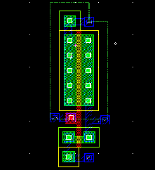
Fig. 12 Layout of CMOS Inverter operating in Subthreshold conduction region.
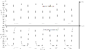
Fig. 14 Post-Layout Simulation – Transient analysis for CMOS Inverter operating in subthreshold conduction region.
For a 1-bit CMOS Full Adder operating in subthreshold conduction region, layout and post-layout simulation results are shown in Fig. 15 and 16 respectively.
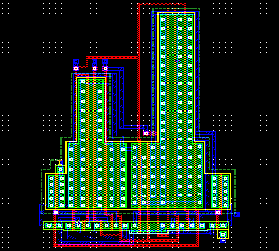
Fig. 15 Layout of 1-bit CMOS Full Adder operating in subthreshold conduction region.
IJSER © 2011 http://www.ijser.org
International Journal of Scientific & Engineering Research Volume 2, Issue 6, June-2011 6
ISSN 2229-5518
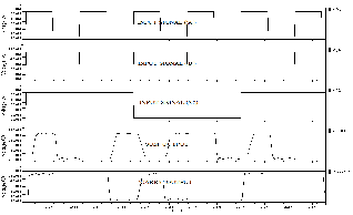
Fig. 16 Post-Layout Simulation – Transient analysis for 1-bit CMOS Full Adder operating in subthreshold conduction region.
Based on the subthreshold conduction region, the designing of a 1-bit CMOS Full Adder has been done. The supply voltage used for the circuits operating in subthreshold conduction region is 0.2 V. The power analysis has also been carried out for the circuits operating in subthreshold conduction region and in strong inversion region. It is found that the circuits operating in subthreshold conduction region provide the significant power reduction than the strong inversion region.
Also, it can be found that subthreshold conduction region is advantageous in applications where power is the main concern and performance can be sacrificed to achieve the low-power because the speed of a circuit operating in subthreshold conduction region becomes significantly slow.
The authors wish to thank Vivek Sharma, Pankaj Kumar, Ritesh Patel and Mohd. Rashid Ansari for their valuable help, criticisms, motivation and precious suggestions during this work.
[1] K. Granhaug and S. Aunet, “Six Subthreshold Full Adder Cells characterized in 90 nm CMOS technology” IEEE Design and Diagnostics of Electronic Circuits and Systems, pp.25-30, 2006.
[2] S. Hanson, B. Zhai, K. Bernstein, D. Blaauw, A. Bryant, L.
Chang, K. K. Das, W. Haensch, E. J. Nowak and D. Sylvester, “Ultralow-voltage, minimum-energy CMOS,” IBM Journal of Research and Development, vol. 50, no. 4-5, pp. 469–490, 2006.
[3] V. Sharma and S. Kumar, “Design of Low-Power CMOS Cell Structures Using Subthresold Conduction Region” International Journal of Scientific and Engineering. Research, vol. 2, Feb 2011.
[4] A. P. Chandrakasan, S. Sheng and R. W. Brodersen, “Low Power CMOS Digital Design,” IEEE Journal of Solid-state Circuits, vol. 27, no. 4, pp. 473-484, April 1999.
[5] H. Soeleman, K. Roy and B. C. Paul, “Robust subthreshold logic for ultra low-power operation,” IEEE Trans.VLSI Syst., vol. 9, pp. 90-99, Feb. 2001.
[6] V. Moalemi and A. Afzali-Kusha, “Subthreshold 1-bit Full Adder Cells in 100 nm Technologies,” IEEE Computer Society Annual Symposium on VLSI, pp. 514-515, May 2007.
[7] K. Ragini and B. K. Madhavi, “Ultra Low Power Digital Logic Circuits in Subthreshold for Biomedical Applications,” Journal of Theoretical and Applied Information Technology, 2005.
[8] K. Roy, S. Mukhopadhyay, and H. Mahmoodi-Meimand, “Leakage current mechanisms and leakage reduction techniques in deep-submicrometer cmos circuits,” in Proceedings of IEEE, vol. 91, no. 2, pp. 305-327, 2003.
[9] A. Wang, B. H. Calhoun and A. P. Chandrakasan, Subthreshold
Design For Ultra Low-Power Systems, Springer, USA, 2006.
[10] R. M. Swanson and J. D. Meindl, "Ion-Implanted Complementary MOS Transistors in Low-Voltage Circuits," IEEE Journal of Solid-State Circuits, vol. 7, no. 2, pp. 146-153, April. 1972.
[11] S. M. Kang and Y Leblebici, CMOS Digital Integrated Circuits:
Analysis and Design, 3rd ed, McGraw Hill, 2004.
IJSER © 2011 http://www.ijser.org