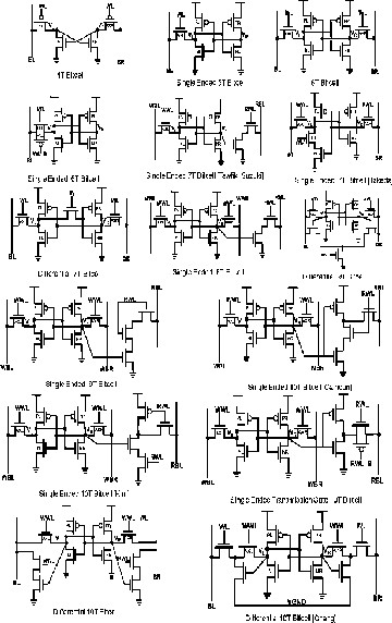
ing of a 6T SRAM, in similar manner the designing variation have been done using 4T to 10T.
1253
Leakage Power Minimisation in memory design using an adaptive technique to optimize the Body Biasing Voltage
Asmita Pattnaik, Kanan Bala Ray
Abstract— Here the discussion and analysis is based on an adaptive technique that has been done using 180nm Technology in Cadence.It is being used with the memory design of 6T SRAM cell for Leakage power minimization in the Standby mode of operation, SNM based calculation to check the stability of the circuit.This Adaptive system used over here to provide an optimal value of the body bias voltage which will increase the threshold voltage and the leakage reduction will occur in whole standby process as well as an effective compensation of the process and temperature variations.
Index Terms— BTBT,CMOS, DIBL,GIDL,Leakage Mechanisms of short channel devices, 6T SRAM,Sub-Threshold Leakage, SNM,Adaptive Reverse Body Bias Techinque.
—————————— ——————————
ccording to Margala(2006), “there is a rapid ment of VLSI and this has decreased the device tries and increased transistor densities of integrated circuits and circuits with high complexities and
high frequencies have been started to emerge but these circuits consume an excessive amount of power and generate an increased amount of heat” [9]. Thus, it is always apparent that circuits with excessive power dissipation are less reliable and more susceptible to runtime errors. Due to these con- cerns, the importance of low power come into picture infront of the designers and improving energy efficiency at all levels of the design.Thus due to low power in memories can im- prove the system power-efficiency, performance, reliability and overall costs.SRAMs are now a days used for designing the low power low voltage memory design especially for all sophisticated electronics devices. Hence further research is going on to achieve more success in this ground, basically on the leakage power minimization. As leakage power minimiza- tion is the most sensitive as well as a dominant feature in the VLSI designing, so it has been taken here as a crucial issue of discussion in this paper. The common problem in all these methods is that they reduce the leakage power only in the standby mode. In this paper a method has been proposed that the reduction must be there in both active as well as standby mode. Here the leakage power reduction has been done using leakage power reduction circuits.
As per previous study which has been done before that SRAM is known for its low standby leakage power, and 95% of area of a system is devoted to its memory. Usually, 6T SRAM also known for its high speed as compared to DRAM. According to the demand of our day to day life we are using the various electron- ics devices which we need to be more portable, less power consuming, less area, high speed and more life span of the
battery. And in those electronic systems some memory devices are also used like RAM, ROM. In case RAM, basically they are of two types SRAM and DRAM. SRAM is faster as compared to DRAM but consumes more Power. These issues are the main aspects of my motivation. The main motive is to design the 6T SRAM circuit which will consume less power and will have high SNM using a low power consuming device. Also the aim is to design a circuit in which power of the 6T SRAM must be re- duced to an acceptable value. Till date whatever paper has been published was based on the standby mode power reduction. So in this paper, the trail is on the reduction of the power in both standby mode as well as active mode by using various tech- niques and power reducing circuits. Here as per the study current generator, current differentiator and an adaptive reverse body bias circuit has been used for the power reduction forming a feedback loop for the target circuit (6T SRAM).
The rest part of paper composed of discussion on related work which is done in previous issue in section 2, includes the dis- cussion on the papers that have been taken as reference and the discussion about all basic concepts of SRAM, its Leakage pow- er and the current components. Section 3, includes the discus- sion on the working of the proposed design for leakage power reduction. Section 4 includes the simulated results of the work.Section 5 is about the Conclusions and finally, the report end with Acknowledgement and References.
There are several designs have been proposed previously
keeping various designing aspects in focus i.e.,density,area, low
IJSER © 2014
ISSN 2229-5518
1254
voltage and timing specification. Fig.1.[6] describes the design-
ing of a 6T SRAM, in similar manner the designing variation have been done using 4T to 10T.
In Fig.1.the architecture of the previously published SRAM bit cell have been shown [4]. In this design of the 4T SRAM have been discussed where circuit is a load less configuration, PMOS devices acts as the access transistors [4].The PMOS OFF- state current is more than the pull-down NMOS transistor leakage current for retaining data '1'. But there is also a draw- back in this design that is with the increasing process varia- tions and exponential dependence of the sub-threshold current on the threshold voltage, satisfying this design requirement across different parameters may be challenging.
In case of the 5T SRAM, it is based on the asymmetric cross-
coupled inverter with a single bit line [4]. The bit line has been pre-charged with separate voltages. Though there been used separate voltages for pre-charge, still then in the intermediate cases of voltages a dc-dc converter in required due which the requirement of additional design margin would be needed for the PVT corners which would violates its applicability.
Then comes the 6T design, in which two cross-coupled invert- ers are connected back to back having two NMOS as the access transistors.Write operation is done by the modulation of the virtual VDD and virtual VSS [4].
In case of the 7T, it has separate read port and the write opera- tion. In case of the single-ended design the write operation have been done either due to asymmetrical inverter character- istics or differential VSS/VCC bias. And during the read opera- tion the extra transistor turned off .When 7T design operates in differential mode the feedback path between the two inverters get cut-off during the write operation [4].
In 8T design, resembles 6T SRAM only there are the extra transistors connected to the later design for the separate read and write operation.
Then for 9T SRAM design the bit-cell is designed with differen- tial read which is considered to be a disturb-free operation [4]. And in 10T design, single-ended resembles the single -ended
8T designs read and write operation.
In this part of the paper a discussion is on the basic compo- nents of the leakage current in CMOS. The Paper which were discussed over here are taken to analyse the leakage power reduction by the use various circuits [1]. As per the previous study which have been done that the analysis is done on the leakage power reduction of various circuit like interrupt con- troller, 12-bit SEC circuit, 16-bit SEC/DED circuit, 12-bit ALU and controller, 9-bit ALU, 32-bit adder/comparator.
IJSER © 2014
ISSN 2229-5518
1255
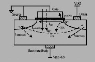
In Fig.2, shown above basically consists of six leakage compo- nents.They are, I gate(GB) and Igate(DG) are the gate-to-bulk and drain-to-gate oxide tunnelling currents;IPT is channel Punch- through current Isub is the sub-threshold current; IGIDL is the gate induced drain leakage; IBTBT(DB) and IBTBT(SB) are the band-to-band tunnelling currents of the drain-to-bulk and source-to-drain junctions respectively due Junction leakage; and IHC is the gate current due to hot carrier effect [1]. The gate leakage,BTBT current and sub-threshold current are the dominating compo- nents in the total leakage. So, when Vds of the cut-off transistors get reduced across the reverse-biased substrate-drain PN junction then other leakage components are considered to be negligible.
The leakage current occurs when the P-N junction in MOSFET is reverse biased and the current which is generated moves from the source or drain towards the substrate.And this is basically happens when the transistors are in OFF state or in otherwords we can say in the STAND BY mode.As the leakge occurs at the junction end it so called as Junction leakge.A P-N junction when get reversed biased the leakage which occurs is due to two major components: a)minority carrier diffusion/drift b)electron-hole pairs.These two components occurs basically in the depletion region. Instantlly, when we provide a low voltage as input to an inverter it gets an high output voltage as , the PMOS is ON state and the NMOS goes to OFF state. Hence, the voltage at the drain-substrate of NMOS is equals to supply voltage.Hence a leakage current gets generated at the drain towards substrate.If both p and n regions are heavily doped, band-to-band tunnelling (BTBT) dominates the p-n junction leakage as the leakage current is also dependent on the doping concentration and area of the diffusion region at the drain end. Junction leakage also depends upon high temperature. Therefore, Junction leakage is negligible as compared to other leakage components.
In MOS transistors the gate induced drain leakage (GIDL) occurs
due to the high field effect in the drain junction. In an NMOS
transistor when the gate is grounded and drain is at VDD, the bend at band gap in the drain generates electron-hole pair by avalanche multiplication and band-to-band tunnelling.As the holes are rapidly moves towards the substrate a deep depletion region is created. So at the same time,as the electrons are present in the drain region and as they are majority factor for current,a current source occurs called GIDL current. Due to the high drain to body voltage and high drain to gate voltage leakage mecha- nism is made worse. The halo implants increases due to the transistor scaling, where the substrate doping at the junction interfaces is increased, while the channel doping is low. Basically, to have control over the punch-through and DIBL when there arises a low impact on the carrier mobility in the channel [3].
The gate direct tunnelling leakage flows from the gate through the “leaky” oxide insulation to the substrate mechanisms for direct tunnelling arises due to hole tunnelling in the valence band and electron tunnelling in the conduction band as well as in the valence band.From all these three electron tunneling at the conduction band is the dominant one. The magnitude of the gate direct tunnelling current increases exponentially with the gate oxide thickness supply voltage VDD and T ox.
“The sub-threshold leakage is the drain-source current of a transistor operating in the weak inversion region which is different from the concept of the strong inversion that drift current dominates, the sub-threshold conduction is due to the diffusion current of the minority carriers in the channel for a MOS device” [12]. Moreover, an inverter produces high output voltage with low input voltage by making the NMOS off. Even though VGS is 0V, t still a current flowing in the channel of the off state NMOS transistor due to the VDD potential of the VDS . The magnitude of the sub-threshold current depends on threshold voltage (VT) and it plays a dominant role as compared to other parameters.
The IOFF is the leakage current when a transistor is in OFF state
(when VGS=0V for an NMOS device).Hence as per the discussion
When VDB = VDD, the IREV and IGIDL increases in there magnitude.
IJSER © 2014
ISSN 2229-5518
1256
Similarly, ISUB increases with VDB because of the DIBL effect due to the short-channel effect [10].Among the three components of IOFF (total leakage current); ISUB is clearly the dominant component. Hence the main target is now to work on ISUB, so that leakage power can get reduced i.e., by decreasing the sub-threshold leakage currents in circuits that are in ACTIVE or STANDBY state [10].
According to Farzan Fallah and Massoud Pedram(2005), “the best way to decreasing the leakage current is by using reverse-body bias (RBB).With the help RBB the threshold voltage can get increased when the transistors is in the STANDBY mode. By reverse biasing a transistor increases its threshold voltage and it can be done during standby, by applying a strong negative bias to the NMOS bulk via a charge pump and connecting the PMOS bulks (N wells) to the VDD rail.But when the reverse body biasing (RBB) is applied to the PMOS transistors by raising the N-well voltages, a triple-well technology, which may not always be available. Because the threshold voltage changes with the square root of the reverse bias voltage, a large voltage may be necessary to get a small increase in the threshold voltage. As a result, this method becomes less effective as the supply voltage is scaled down.On the positive side, with RBB, the IC logic state is retained while in the STANDBY mode, allowing operation to resume where it suspended [10]”.
The SRAM cell incorporates a static latch, comprising two cross-coupled inverters, so that it does not require periodic refreshing to retain the stored information, provided that there is adequate power supply voltage for the cell (VDD, cell).
In which the two cross coupled inverters are connected back- to-back (there are two PULL UP transistors and two PULL DOWN transistors).There are two access transistors. When the horizontally-running word-line (WL) is enabled (i.e., a row is selected in an array), the access transistors are turned on, and connect the storage nodes to the vertically-running bit-lines (BL and BL). In other words, they allow access to the cell for read
and write operations, acting as bidirectional transmission gates.
The 6T SRAM design 1) READ operation-the bit-lines are pre-charged to high voltage VDD and the word line is selected to high value. And then the word-line is selected (pulsed to a high level). On the side of the cell storing a logical ‘0’ (i.e., a low voltage), the bit-line is discharged via the pass-gate transistor and pull-down transistor, so that a differential voltage develops between the bit-lines. This differential voltage should be large enough for a sense amplifier to detect the state of the cell. The differential voltage should not be too large, however; otherwise the cross-coupled inverters could flip their state. (The read operation should be non-destructive.) The cell beta ratio, which is the ratio of the strength (drive current) of the pull-down transis- tor to that of the pass-gate transistor, should be sufficiently large to ensure that such a read disturbance does not occur.
(2) WRITE operation, the bit-lines are driven to complemen- tary voltage levels via a write driver and then the word-line is selected. On the side of the cell for which the bit-line voltage is logical ‘0’ (i.e., a low voltage), the internal storage node is discharged through the pass-gate transistor. The cross-coupled inverters raise the voltage on the opposite storage node and latch the cell. The discharging strength of the pass-gate transistor must overcome the restoring strength of the pull-up transistor. The cell gamma ratio, which is the ratio of the strength of the pass-gate transistor to that of the pull-up transistor should be sufficiently large to ensure that write failure does not occur.
(3)STANDBY, means when the word line is not asserted, and then the two access transistors disconnect the cell from the bit lines. The two cross-coupled inverters formed by four transistors will continue to reinforce each other as long as they are connected to the supply.
As per the study in the year 1987, the most important metric for
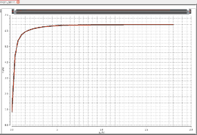
the SRAM is the read stability of the circuit, which is in other word called the Static Noise Margin (SNM). SNM is the maxi- mum tolerable DC noise voltage at a storage node that does not cause a read disturbance, and it is the length of the diagonal of the largest square that can fit into the “eyes” of the butterfly curves, i.e., the read voltage transfer characteristics (VTC), for the SRAM.
IJSER © 2014
ISSN 2229-5518
1257
As per the study of Shelendra Singh Tomar, Madhav Singh and Shyam Akashe (2011)” The "butterfly" curve used to measure the static noise margin. The static noise margin of SRAM cell de- pends upon the cell ratio (CR), supply voltage and also on the PULL- UP ratio. For stability of the SRAM cell, good SNM is required which depends upon the cell ratio, supply voltages and the PULL-UP ratio. CELL ratio is the ratio between the sizes of the driver transistor to the load transistor during the read operation. PULL-UP ratio is the ratio between the sizes of the load transistor to the access transistor during the write opera- tion” [11].
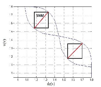
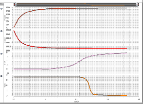
The modulation of the power supply voltage the SRAM cell gets affected on the ground of its stability.The SNM also depends upon the supply voltage (Vdc), from previous analysis the SNM value increases as the we increase the supply voltage, basically during the read operation.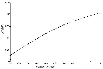
Fig.5 The graph demonstrates that the SNM value increases if the supply voltage get increased.
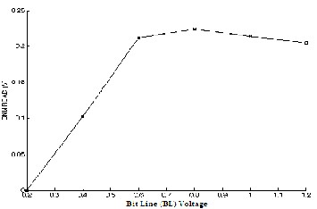
Bit-line voltage modulation is calculated by pre-charging bit- lines at the full power supply voltage. In Fig.6 the graph demon- strates the value of SNM improves by decreasing bit -line voltage as compared to the Vdc variations during the read operation.
IJSER © 2014
ISSN 2229-5518
1258
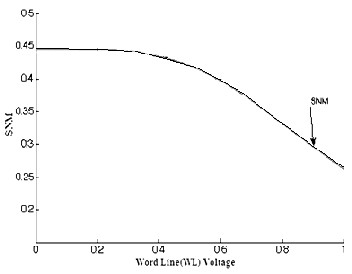
In the Fig.7 as per the analysis shown that, the minimization of maximum voltage so that the swing of the word-line to sustain the cell access transistor during the read operations [8].The word line voltage when get reduced the SNM get in- creased during the read operations with respect to the supply voltages.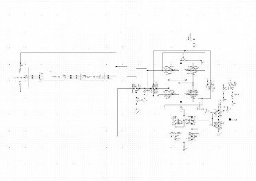
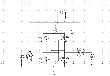
In the Fig.8.where the 6T SRAM is connected to the peripheral circuits, which includes three different circuits: 1) current
differerence generator circuit 2) current comparator 3) body bias
regulator circuit.The output generated from the body bias regulator is again fed back to the current difference generator circuit.The loop goes on till an optimal value is generated as Vbody. This Vbody will provided to the target circuit i.e., 6T SRAM as a input. The Optimal value of the Vbody will increase the VTH of the transistor in SRAM and the leakage power will get reduced as the circuit operates at high threshold.
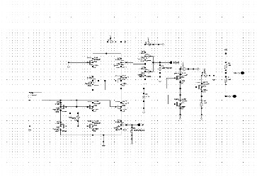
CURRENT DIFFERENCE GENERATOR CIRCUIT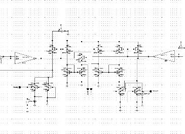
Fig.8 Schematic of the Current difference generator circuit.
The Current difference generator circuit has curremt mirror circuit and current differential amplifier circuit which will produce the two different current that is ∆I1=I1-I2 and ∆I2= I2-I1. Hence , ∆I1= - ∆I2. There are two cluster circuits connected to the drain end of the current mirror so that the current will get replicated.
CURRENT COMPARATOR CIRCUIT
The current comparator circuit as shown in Fig.9 is getting its input from the current difference generator circuit which is preceding to the respective circuit.As the comparator circuit work as a class AB amplifier, so two different output is generated as UP and DOWN signal through four different logic gates.These outputs will be fed as inputs to the successive circuit, which is the charge pump circuit along with its output stage.
IJSER © 2014
ISSN 2229-5518
1259

The charge pump circuit gets input from the comparator as UP and DOWN signal. As the capacitor connected to it gets charged and discharged it produces output in the form of two different voltages at its output stage.
The whole design has to satisfy three conditions:
1)I1 < I2, UP=0 & DOWN =1, V body decreases to reduce the total leakage.
2) I1> I2, UP=1 & DOWN = 0, output of vbody regulator
increases.
3) I1 = I2, ∆I1=0 =∆I2, then an optimal value of the body bias found and that is to be maintained.
Finally, the optimal value of as Vbody will be maintained and supplied as input to 6T SRAM which is the target circuit to minimize the leakge by caluclating it from leakge current which is taken from the OFF state transistors.
PLEAKAGE = ILEAKAGE * VDD.
The Total power consumption also gets reduced by use of this technique of adaptive reverse body bias.
Leakage current also get reduce to about 6.023pA.
The result is discussed in the tabular form showimg the mini-
mum leakage power.
IJSER © 2014
ISSN 2229-5518
1260
CIRCUIT DESIGN | Leakage Power | SNM |
conventional 6T SRAM | 924.5E-6 | 463.23 mV |
6T SRAM with sense amplifier | 693.3E-6 | 416.07 mV |
6T SRAM with ARBB circuit | 11.05E-12 | 491.44 mV |
This paper gives a summary that as the leakage power is an important aspect and it plays a dominant role in the total power of the design. Therefore, more attention have to be paid to the standby leakage power.The leakage can also be reduced if we do constant field scaling i.e., by reducing the supply, thethreshold increases but it remain fixed at acertain value and beyond it we can increase just by providing it a reverse body bias.But again there a problem to increase the threshold to which value,hence to get an optimal condition the Adaptive Body Bias in an rec- ommendable techniques which after following an feedback loop and satisfying certain condition will provide an optimal value as body voltage to the target circuit transistors. So, in this manner the threshold increases and leakage reduces without any violation to the performance of the target circuit.
First of all I would like to thank my guide Assistant Prof. Kanan Bala Ray & Prof. S.K. Mandal, Controller Examination, Electronics & Electrical Engineering Department, School of Electronics Engineering, KIIT University, Bhubaneswar for guiding me throughout the research part of the thesis. I really am privileged to have opportunity to work with him.I will also thank Assistant Prof. J.K. Das in my research work. I am also thankful to all the staffs & employees of School of Elec- tronics Engineering, KIIT University. Also I want give my deep sense of gratitude to the incharge of Cadence Lab and to all my friends and classmates for their support.
[1] Liyi Xiao,Chang Liu, Yu Sun.“ A Novel Adaptive Reverse Body Bias Technique to Minimize Standby Leakage Power and Compensate Process and Temperature Variations”,IEEE Cross Strait Quad-Regional Radio Science and Wireless Technology Confer- ence, 2011.
[2]Kumkum Verma,Sanjay Jaiswal, Dheeraj Jain, “Design & analysis of 1Kb 6T SRAM using different architecture.”,IEEE fourth international conference on computational network and com- munication network,2012.
[3] Anupriya Jain, “Analysis and Comparison of Leakage Reduc- tion Techniques for 6T-SRAM and 5T SRAM in 90nm Technolo-
gy” ,International Journal of Engineering Research & Technology
(IJERT), Vol. 1 Issue 6, August – 2012.
[4] Kulkarni, Jaydeep P., and Kaushik Roy,“Ultralow-Voltage Process-variation-Tolerant Schmitt-Trigger-Based SRAM De- sign",IEEE transactions of VLSI systems, vol. 20, No. 2.,February
2012
[5]Balachandrana. A, “ Low power and area efficient static random access memory design using Schmitt Trigger.”
[6]Changhwan Shin, "Advanced MOSFET Designs and Implica- tions for SRAM Scaling".
[7]HeungJun Jeon, Yong-Bin Kim, and Minsu Choi, “Standby Leakage Power Reduction Technique for Nanoscale CMOS VLSI Systems.”, IEEE Transactions on Instrumentation and Measure- ment,Vol.59,No.5,May 2010,
[8]Kyung Ki Kim and Yong Bin Kim, “A Novel Adaptive Design Methodology for Minimum Leakage Power Considering PVT Variations on Nanoscale VLSI Systems", IEEE Transaction on Very Large Scale Integration(VLSI) Systems,Vol.17,No.4,April 2009,
[9]Martin Margala, "Low Power Memory Circuits", 2006, In
Wai Kai Chen, Ed, ‘The VLSI Handbook’, 2nd ed, p. 57,
[10]Farzan Fallah, San Jose and Massoud Pedram,” Standby and Active Leakage Current Control and Minimization in CMOS VLSI Circuits “, IEICE Transaction on Electronics, Vol.E88-C, No.4, pp-509-519, April 2005.
[11] Shelendra Singh Tomar, Madhav Singh,and Shyam Akashe,
”Static Noise Margin Analysis during Read Operation of 7T
SRAM Cells in 45nm Technology for Increase Cell Stability”,
IJEST, Vol. 3, No. 9, September 2011.
[12]Vijay Kumar Sharma and Surender Soni ," Lowpower
IJSER © 2014
ISSN 2229-5518
1261
CMOS Inverter Design at different technologies", International
Journal of Applied Engineering Research,Vol. 1 No.3, 2010.pp.372-
381.
Asmita Pattnaik is currently pursuing masters degree program in VLSI & Embedded System Design in KIIT Universi- ty,asmita027@gmail.com.
Kanan Bala Ray is currently pursuiung PH.D in VLSI & Embed- ded System Design in KIIT university,bikashkanan@gmail.com.
IJSER © 2014