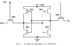
The schematic of SRAM cell is shown in the Fig.1. It
International Journal of Scientific & Engineering Research, Volume 5, Issue 2, February-2014 938
ISSN 2229-5518
T.SANKARARAO STUDENT OF GITAS,
S.SEKHAR DILEEP ASST PROF GITAS,
P.ADITYA ASST PROF GITAS
Abstract: The growing demand for high density VLSI circuits the leakage current on the oxide thickness is becoming a major challenge in deep-sub-micron CMOS technology. In deep submicron technologies, leakage power becomes a key for a low power design due to its ever increasing proportion in chip‟s total power consumption. Motivated by emerging battery-operated application on one hand and shrinking technology of deep sub micron on the other hand, leakage power dissipation is playing a significant role in the total power dissipation as threshold voltage becomes low. Due to the trade-off between power, area and performance, various efforts have been done. This work is also based to reduce the power dissipation of the VLSI circuits with the performance up to the acceptable level. Here we proposed Novel SRAM architecture called IP-SRAM with separate write sub-cell and read sub-cell. In this paper we designed the total 8 bit SRAM architecture with newly proposed techniques and compare this one with conventional SRAM architecture and we observed that the total power consumption is reduced. Here the total architecture was designed with 180nm technology. These results are compared this with deep submicron technologies.
Keywords: SRAM, Deep Submicron Technology, Sub Threshold Leakage Power
—————————— ——————————
SRAMs strongly impact the over- all power, performance, stability and area requirements. In order to manage constrained tradeoffs, they must be specially designed for target applications because The Static Random Access Memory (SRAM) is a critical component in the modern Digital Systems-on-Chip (SoCs) [1]. Rapid growth in semiconductor technology has led to shrinking of feature sizes of transistors using deep submicron (DSM) process. As MOS transistors enter deep submicron sizes, undesirable consequences regarding power consumption arise. Until recently, dynamic or switching power component dominated the total power dissipated by an IC. Voltage scaling is perhaps the most effective method to decrease dynamic power due to the square law dependency of digital circuit active power on the supply voltage.
As a result, this demands a reduction of threshold
voltage to maintain performance. Low threshold voltage results in an exponential increase in the sub- threshold leakage current. On the other hand as technology scales down, shorter channel lengths result in increased sub-threshold leakage current through an off transistor. Therefore, in DSM process static or leakage power becomes a considerable proportion of the total power dissipation. For these reasons, static power consumption, i.e. leakage power dissipation, has become a significant portion of total power consumption for current and future silicon technologies.
Here we present some VLSI techniques to reduce leakage power. Each technique provides an efficient way to reduce leakage power. In this paper we designed SRAM cell [2].with low power techniques with 180nm technology and compare with conventional SRAM cell
II.CONVENTIONAL 6-T SRAM CELL
Static Random Access Memory (SRAM) to be one of the most fundamental and vitally important memory technologies today. Because they are fast,
robust, and easily manufactured in standard logic processes, they are nearly universally found on the same die with microcontrollers and microprocessors. Due to their higher speed SRAM based
Cache memories and System-on-chips are commonly used. Due to device scaling there are
IJSER © 2014 http://www.ijser.org
International Journal of Scientific & Engineering Research, Volume 5, Issue 2, February-2014 939
ISSN 2229-5518
several design challenges for nanometer SRAM design. Low power SRAM design is crucial since it takes a large fraction of total power and die area in high performance processors. A SRAM cell must meet the requirements for the operation in submicron/nano ranges. The scaling of CMOS technology [3] has significant impacts on SRAM cell random fluctuation of electrical characteristics and substantial leakage current.
The schematic of SRAM cell is shown in the Fig.1. It
The dual inverter latch is heart of the SRAM cell [5]. Each end of the latch holds a value that is the
has 2 pull up PMOS and 2 NMOS pull down transistors as two cross coupled inverters and two 2
NMOS access transistors to access the SRAM cell during Read and Write operations [4] . Both the bit lines (BL and BLB) are used to transfer the data during the read and write operations in a differential manner. To have better noise margin, the data signal and its inverse is provided to BL and BLb respectively. The data is stored as two stable states, at storing points VR and VL, and denoted as 0 and 1.
complement of the other side.
In power gated leakage feedback with stack, we are combining two techniques i.e. leakage feedback approach due to less transistor than sleepy-stack in which we replaces each transistor in base case into
three transistors, and ultra low power technique i.e. Stack approach, here we are combining these two techniques.
IJSER © 2014 http://www.ijser.org
International Journal of Scientific & Engineering Research, Volume 5, Issue 2, February-2014 940
ISSN 2229-5518
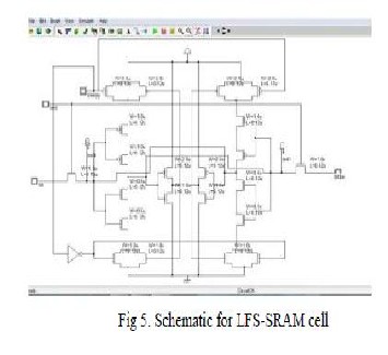
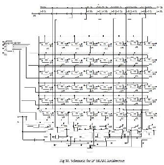
In the novel power gated Improved P3 (IP) SRAM Cell, the combination of two separate sub - cells (write and read) structure is proposed with a pMOS gated ground and drowsy scheme to reduce the active and standby power without losing the cells‟ performance. The data write and memory storage is being done at upper sub -cell
while lower sub-cell is used for data- read operation, only. In the active mode of operation, the cell is supplied with VDD [6]. In data write mode, the data read sub-cell is completely isolated from the data write sub- cell through BL‟s and vice-versa, which further improves the cell‟s stability.
IJSER © 2014 http://www.ijser.org
International Journal of Scientific & Engineering Research, Volume 5, Issue 2, February-2014 941
ISSN 2229-5518
A general SRAM Architecture and its peripherals are shown in below. The SRAM array consists of rows and columns of bit cells. For small caches, it is possible to place a word of data in a row; however, in large memories because of limitation, it is necessary to arrange several words of data in each row [7]. Cells of each column share the same Before the read access, the bit lines are recharged to a known value by the recharge circuits. The row decoders are use to select a row in the array. Depending on the mode of operation, storage Celle the are connected the bit lines and either the stored data in the cell is read by sense amplifiers
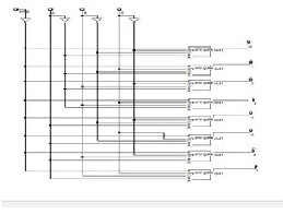
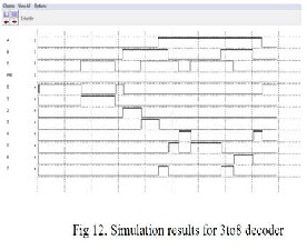
Fig 11. Schematic for 3to8 decoder
or overwritten for the write circuits and large multiple blocks of the same array are used such that an extra address generator called block address decoder is required.
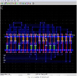
A row decoder is used to decode the input address and select the word line. When performing a write or read operation only one of the row is selected and 8 bits of data is transmitted. The row decoder selects one of those rows, depending on the 3 bit address given to it. In order to design an 8x8 SRAM a 3x8 decoder [8] is used. Number of word line equals to the number of rows in the SRAM cell array [9].
IJSER © 2014 http://www.ijser.org
International Journal of Scientific & Engineering Research, Volume 5, Issue 2, February-2014 942
ISSN 2229-5518
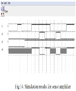
A sense amplifier circuit is used to read the data from the cell. In addition, it helps reduce the power consumption in the overall SRAM chip by sensing a small difference in voltage on the bit lines. For having high performance SRAMs, it is
the design.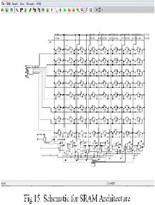
essential to take care of the read speed both in the cell-level design and in the design of a clever sense amplifier. Need for larger memory capacity, higher speed, and lower power dissipation impose trade offs in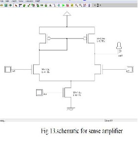
IJSER © 2014 http://www.ijser.org
International Journal of Scientific & Engineering Research, Volume 5, Issue 2, February-2014 943
ISSN 2229-5518
IJSER © 2014 http://www.ijser.org
International Journal of Scientific & Engineering Research, Volume 5, Issue 2, February-2014 944
ISSN 2229-5518
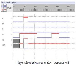
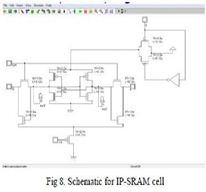
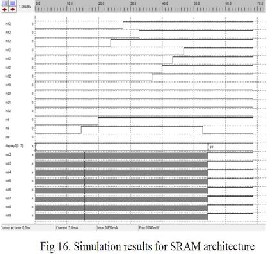
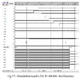
Figure 18 is the Schematic of IP-SRAM Architecture and Figure 17 shows the simulation results of IP-SRAM. From these results it is clear that because of keeping the separate write sub cell and read sub cell the power consumption for
In this paper we designed SRAM architecture with IP-SRAM technique to reduce power consumption. In this IP- SRAM technique we have separate read and write operations and we are placing one PMOS device in between pull down network and ground to reduce power consumption. Here the total SRAM architecture was designed using 180nm
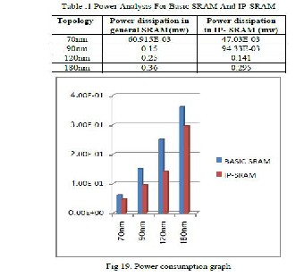
IP-SRAM is substantially reduced. Table
-1 shows clearly that for 70nm, 90nm,
120nm and 180nm technologies the power consumption is reduced very much for IP-SRAM when compared with the basic SRAM.
X.CONCLUSION
technology and we observed the IP- SRAM architecture have less power consumption compared to basic SRAM architecture.
Hence it is concluded that the proposed SRAM Architecture is used for low power designs and these designed techniques are used for high performance and low power applications.
[1]International Technology Roadmap for
Semiconductors,2003. http://www.publicitrs.net.
[2]C.-H. Lo and S.-Y. Huang, “P-P-N Based 10T SRAM Cell for
Low-Leakage and Resilient Sub threshold Operation,” IEEE Journal of Solid-
State Circuits, Vol. 46, No. 3, 2011, pp. 695-704.
[3]N. Kr. Shukla, R. K. Singh and M. Pattanaik, “A Novel
Approach to Reduce the Gate and Sub-threshold Leakage in a
Conventional SRAM
Bit-Cell Structureat Deep-Sub Micron CMOS Technology,”
International Journal of Computer Applications (IJCA), Vol. 23, No. 7, 2011, pp.
23-28.
[4]L.-J. Zhang, C. W u, Y.-Q. Ma, J.-B. Zheng and L.-F. Mao, “Leakage Power Reduction Techniques of 55 nm SRAM Cells,” IETE Technical
Review, Vol. 28, No. 2, 2011, pp. 135-145
[5]K. Zhang (Ed.), “Embedded Memories for Nano-Scale VLSIs,” Integrated Circuits and Systems Series, Springer. [6]Designing an SRAM array at the 90nm CMOS tech node Shrivathsa Bhargav and Jaime Peretzman ELEN 4321 - Digital VLSI circuits Columbia University, Fall 2007.
[7]B.S. Deepaksubramanyan and Adrian Nu˜nez EECS Department,Syracuse University , Analysis of Subthreshold Leakage Reduction inCMOS Digital Circuits, Proceeding of the
13TH NASA VLSISymposium Post Fall, IDAHO, USA, June
2007.
[8]Park, J. C., and Mooney III, V. J. “Sleepy Stack Leakage
Reduction.Very Large Scale Integration (VLSI) Systems,” IEEE Transactions vol.14,no.11, pp.1250-1263, November
2006.
[9]Kao, J. T., and Chandrakasan, A. P. “Dual-Threshold
Voltage Techniques for Low-power Digital Circuits,” IEEE Journal of Solid- State Circuits, vol.35, no.7, pp.1009-1018.
IJSER © 2014 http://www.ijser.org