International Journal of Scientific & Engineering Research, Volume 5, Issue 2, February-2014 121
ISSN 2229-5518
Implementation of Automatic Testing System for
Microprocessor Using Logic Analyzer
Dr. Mohamed Saad Zaglool, Engineer Mohamed Saleh
Abstract— This paper is about design of inexpensive technique, to develop new methodologies to solve the difficult challenges facing us today in various processor and SOC design environments. In the past few years, some work has been done on exploiting techniques from test to solve problems in verification and vice versa. Adding to that this research is to provide success in providing an ideal environment for cross-examination of test and verification experiences and innovative solutions for testing Microprocessor using logic analyzer. This thesis is about design of inexpensive method for testing environment that simplifies functional testing of Microprocessor and complete circuit tester. This environment consists of the tester hardware and its corresponding software which enables engineers to experience the challenges of testing and debugging without the expense of costly commercial hardware testers. Simple digital circuits can be constructed using breadboards, wires, and DUTs, then tested using switches and LED's. However, advanced Microprocessor are often too complex to be tested, and debugged in this way, due to the large amount of state they may require and the larger number of input and output signals compared with simple projects. So this system in our study can be used to test complex Microprocessor. The system is described as the design and implementation of a compact, small, cheap, low-power and complete circuit tester. Logic analyzer is used in wide scale of testing digital circuits where it can observe the state of the digital circuits. The Logic analyzer consists of two analyzers. The first part is timing analyzer and the second part is state analyzer. Each has specific functions. Logic analyzer is used to detect the fault in 6802
Motorola microprocessor program In this paper, a high level quick checking method, known as Linear Checking Method can be used to qualify the functionality of a Microprocessor. This can also be used to check hard faults in Memory chips.
.Index Terms— Automatic testing; Circuit faults; Circuit testing; DH-HEMTs; Integrated circuit modelling; Logic testing; Microprocessors; Registers; Software testing; System testing.
—————————— ——————————
HE The purpose of this paper is to discuss the possible test techniques available to help the reader determine which techniques will be most effective for his/her skill level and avail- able technology. [1] Logic analyzer is used in wide scale of test- ing digital circuits where it can observe the state of the digital circuits. The Logic analyzer consists of two analyzers. The first part is timing analyzer and the second part is state analyzer. Each has specific functions. Logic analyzer is used to detect the
fault in 6802 Motorola microprocessor program.
Rapid advances in areas of nanometer electronic technology and design automation tools enabled engineers to design larger and more complex digital circuits. Recently, most electronic systems consisted of one or multiple printed circuit boards, containing multiple ICs each. Advances in IC design methods and technolo- gies allow integrating these complex systems into one single IC. These developments are driving engineers toward new SoC de- sign methodologies. SoC is seen as a major new technology and the future direction trend for the semiconductor industry. With- in the next several years, SoC designers will reduce product de- velopment cycle time and place the power in the hands of SoC designers. On the other hand, the more complex are getting electronic systems, the more important become problems of test and design for testability. This is because costs of verifica- tion and testing are getting the major component of design. Today, design and testing are no longer separate issues.
——————————————
Dr. M.S.Zaghloul, Arab Academy for Science, Technology, and Maritime Transport (E-mail: dr_mszaghloul@yahoo.com) Electronic and Communication Department, P.O.1029
The emphasis on the quality of shipped products, coupled with the growing complexity of system design, requires testing issues to be considered early in the design process. At present, most VLSI and system designers know little about testing, so that companies frequently hire test experts to advise their designers on test problems, and they even pay a higher salary to the test experts than to their VLSI designers, this reflects the today’s university education where everyone learns about design, but only truly dedicated engineers learn about testing. Entering into the SoC era means that test must now become an integral part of the VLSI and the system design. The next generation of engi- neers involved with VLSI technology should be made aware of the importance of test. They must be specially trained in test technology to enable them to produce high quality defect-free products [2].
The complete process of circuit design, simulation, implementa- tion, test, and debug are hard tasks. Even though design descrip- tion tools and circuit compilers have kept up with the increasing levels of integration found in current implementation media such as FPGAs and microcontrollers, it has become increasingly difficult to test and debug the complex hardware projects ena- bled by these modern tools and devices. Digital logic implemen- tation technologies emphasize very high levels of integrtion in various forms such that custom VLSI chips, microprocessor, mi- crocontrollers, and field programmable logic such as FPLDs and FPGAs. For faulty ship the user can not repair the chip. Hence
IJSER © 2014 http://www.ijser.org
International Journal of Scientific & Engineering Research, Volume 5, Issue 2, February-2014 122
ISSN 2229-5518
the users have only two choices: either to continue using the chip with a particular failing function, knowing that the failing function will not be used in the given application or to replace the whole chip. Highly integrated circuits have many advantages, such as lower power, reduced circuit board area, greater func- tionality, and lower production cost. However, these circuits require more time and money to be invested into complex de- velopment tools .The process of circuit design involves several distinct steps:
1. First, the designer specifies the circuit at the appropriate level of abstraction. A circuit can be specified in many dif- ferent ways, including high-level hardware description lan- guages, schematics, and behavioral models. Hierarchy in the description is helpful for specifying a design in a top-down fashion. Encapsulating a part of the circuit makes it easy to repeat, much like a subroutine in software makes part of the program easy to invoke iteratively or recursively.
2. Second, modern design tools compile the descriptions into a form suitable either for simulation or hardware implemen- tation. Because less expensive than actual circuit construc- tion, simulation is used to validate and debug a design, and reduces the amount of time needed to debug a hardware implementation.
3. The third step is to implement a circuit prototype that can be tested and debugged.
4. The final step is building real hardware to ensure the fun- damental concepts which meets the required specification.
In recent years, modern circuit design tools have been intro-
bles to experience the challenges of testing and debugging with- out the expense of costly commercial hardware testers.
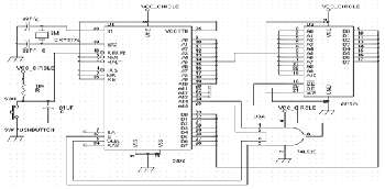
For our work implementation the MC6802 microprocessor is connected with EEPROM memory by connecting the address and data bus as shown in figure 1
Fig. 1 Schematic of microprocessor circuit 6802 Motorola
Most of wiring connecting the 8 data pins and 11 address pins of the memory to the corresponding pins of the processor.
Two NAND gate inputs at each device (A14 and A15) could select
22 or 4 different devices. If A0 through A10 are used for address
selection and A14 through A15 are used for chip selection, the three lines A11-A13 are not used for anything, and they can as-
3
duced to engineers in digital design. The availability of these
sume any of 2
or 8 different states without affecting the chip or
tools has greatly increased the complexity of projects that engi- neers are able to undertake. Unfortunately, the tools available for testing and debugging have lagged behind the tools for speci- fication, compilation, simulation, and implementation.
Simple digital circuits can be constructed using breadboards,
wires, and simple ICs, and then perform the test using switches and LEDs. However, advanced digital circuits using FPLDs and FPGAs are often too complex to be tested and debugged in this way due to the large amount of state they may require and the larger number of input and output signals compared with simple digital circuits [3]. The increasing complexity of VLSI circuits and transition to SoC or even NoC model have made test generation one of the most complicated and time consuming problems in the domain of digital design. Commercial CAD systems for VLSI design and test are both costly and do not provide a good varie- ty of competing or complementary approaches to a given par- ticular problem. It is good for a designer but not for a researcher whose main goal is the search for new efficient solutions. During the last decade, many different low-cost tools running on PCs have been developed to fill this gap. They usually include the major basic tools needed for IC design such that schematics cap- ture, layout editors, simulators, and place and route tool [4]. An inexpensive digital circuit tester simplifying the test and debug experience is introduced in our study. This environment, consist- ing of the tester hardware and its corresponding software, ena-
address selection of the EEPROM.
The MC6802 has 128 bytes of internal RAM (read/write memory) which is fully decoded for addresses (0000 to 007F); this RAM is enabled if pin 36 is high and disabled if it is low.
The low 32 bytes of RAM are separately powered from pin 35 (5
V at 8mA) to permit a battery supply to save critical data during power down [6]. The image for the circuit is shown in figure -2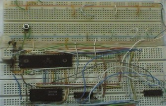
Fig. 2 Image of microprocessor circuit 6802 Motorola
IJSER © 2014 http://www.ijser.org
International Journal of Scientific & Engineering Research, Volume 5, Issue 2, February-2014 123
ISSN 2229-5518
The EEPROM programmer circuit is used to download the assembly program on the EEPROM 2816A (2 k EEPROM) as shown in figure 5.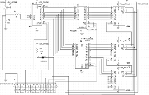
Fig. 3 Schematic diagram of EEPROM programmer
The image of EEPROM programmer is shown in figure 6.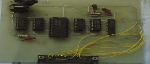
Fig. 4 Image of EEPROM programmer
The 74LS20 NAND gate is used simply as a driver for the LED
as shown in figure 7.
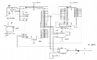
Fig. 5 schematic of programmable lamp flasher
The program of the programmable lamp flasher is given below at table -1.
TABLE 1
The code of program
Address | OP code | operand | label | mnemonic | operand | cycles |
0000 | CE | 40 00 | ON | LDX | #$4000 | |
0003 | 09 | LOOP1 | DEX | 4 | ||
0004 | 27 | 03 | BEQ | OFF | 4 | |
0006 | 7E | 00 00 | JMP | LOOP1 | 3 | |
0009 | CE | 80 00 | OFF | LDS | #$8000 | |
000C | 09 | LOOP2 | DEX | |||
000D | 27 | 03 | BEQ | GO ON | ||
000F | 7E | 00 0C | JMP | LOOP2 | ||
0012 | 7E | 00 00 | GO ON | JMP | ON |
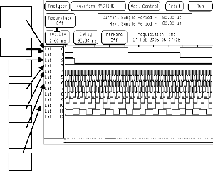
It consists of two delay loops, one which keeps address line A4 high, and second which keeps A4 low. The loops count down the X register to produce longer delays than are possible by counting 8-bit RAM location. The length of the ON and OFF times can be changed independently simply by changing the immediate values that are loaded to X before the first and the second loop respectively. The maximum delay is about 1.4 seconds in each loop [6].The bit pattern of the program is shown in table -2
TABLE 2
Bit pattern of the program
IJSER © 2014 http://www.ijser.org
International Journal of Scientific & Engineering Research, Volume 5, Issue 2, February-2014 124
ISSN 2229-5518
Clk
Reset
A1
A2
A3
A4
A5 Fig. 6 Tming of the program
MACHINE 1 - State Listing
Label > CLK1 RST2 ADDRES DATA Base > Hex Hex Hex Hex
0 1 1 FFFE 00
1 1 1 FFFE 00
2 1 1 FFFE 00
3 1 1 FFFE 00
4 1 1 FFFF 00
5 1 1 FFFF 00
6 1 1 FFFF 00
7 1 1 FFFF 00
8 1 1 0000 CE
9 1 1 0000 CE
10 1 1 0000 CE
11 1 1 0000 CE
12 1 1 0001 40
13 1 1 0001 40
14 1 1 0001 40
15 1 1 0001 40
16 1 1 0002 00
17 1 1 0002 00
18 1 1 0002 00
19 1 1 0002 00
20 1 1 0003 09
21 1 1 0003 09
22 1 1 0003 09
23 1 1 0003 09
24 1 1 0004 27
25 1 1 0004 27
26 1 1 0004 27
27 1 1 0004 27
28 1 1 0005 03
29 1 1 0005 03
30 1 1 0005 03
31 1 1 0005 03
32 1 1 0006 7E
33 1 1 0006 7E
34 1 1 0006 7E
35 1 1 0006 7E
36 1 1 0007 FF
37 1 1 0007 FF
38 1 1 0007 FF
39 1 1 0007 FF
40 1 1 0008 DA
41 1 1 0008 DA
42 1 1 0008 DA
43 1 1 0008 DA
44 1 1 0009 CE
45 1 1 0009 CE
46 1 1 0009 CE
47 1 1 0009 CE
48 1 1 000A 80
49 1 1 000A 80
50 1 1 000A 80
51 1 1 000A 80
52 1 1 000B 00
53 1 1 000B 00
54 1 1 000B 00
55 1 1 000B 00
56 1 1 000C 09
57 1 1 000C 09
58 1 1 000C 09
59 1 1 000C 09
60 1 1 000D 27
61 1 1 000D 27
62 1 1 000D 27
63 1 1 000D 27
64 1 1 000E 03
65 1 1 000E 03
66 1 1 000E 03
67 1 1 000E 03
68 1 1 000F 7E
69 1 1 000F 7E
70 1 1 000F 7E
71 1 1 000F 7E
72 1 1 0010 FF
73 1 1 0010 FF
74 1 1 0010 FF
75 1 1 0010 FF
76 1 1 0011 E3
77 1 1 0011 E3
78 1 1 0011 E3
79 1 1 0011 E3
80 1 1 0012 7E
81 1 1 0012 7E
82 1 1 0012 7E
83 1 1 0012 7E
84 1 1 0013 FF
85 1 1 0013 FF
86 1 1 0013 FF
87 1 1 0013 FF
IJSER © 2014 http://www.ijser.org
International Journal of Scientific & Engineering Research, Volume 5, Issue 2, February-2014 125
ISSN 2229-5518
88 1 1 0014 D7
89 1 1 0014 D7
90 1 1 0014 D7
91 1 1 0014 D7
MACHINE 1 - State Listing
Label > CLK1 RST2 ADDRES DATA Base > Hex Hex Hex Hex
This fault causes the program to start light the led and then go to OFF all the time.
Other example of microcontroller and its board in figure 3 is embedded design for a single board computer SBC8600B which has an expansion board to carry the Mini8600B. The flexible de- sign allows the fast and easy way of realizing and upgrading the controller’s capabilities. In additional to those features offered by Mini8600B, the SBC8600B features 5 serial ports (including (2) RS232 and (3) TTL), 2 USB Host and 1 USB OTG, 2 Ethernet ports, CAN, RS485, LCD, Touch screen, Audio, ADC and more other peripherals. The SBC8600B is a ready-to-run platform to support for Linux 3.2.0, Android 2.3 and WinCE 7 operating sys- tems , - 720-MHz TI AM3359 ARM Cortex-A8 microprocessor- On Board 2*256MByte DDR3 SDRAM + 512MByte NAND Flash .all the data shown for Mini8600B Processor are belong Embest reference. [7]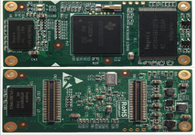
Fig. 7 Mini8600B Processor Card [7]
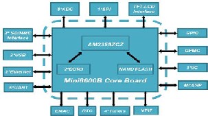
Fig. 8 Mini8600B Function Block Diagram [7]
CONCLUSION
The system is inexpensive yet versatile for testing microcontrol- ler and microprocessors, and subsystems. The component cost is very low comparable to the function which it executes. It is used as a hardware test bench using logic analyzer development envi- ronment. It can be used to test variety of projects using highly integrated logic such as microcontrollers and custom chips. [8]
IJSER © 2014 http://www.ijser.org
International Journal of Scientific & Engineering Research, Volume 5, Issue 2, February-2014 126
ISSN 2229-5518
The implementation of the tester increases the circuit density and reduces the cost. Besides making it possible to add features and fix design bugs long after printed-circuit board were fabri- cated. the system consumes little power and sink only a few milliamperes per pin. The number of wires the engineers must install on the tester's socket is limited to the power and ground connections as the tester maps the remainder of the pins through the microprocessor. This feature improves the setup and reduces the time; as a result, engineers are encouraged to test more often and more completely. Designing straightforward programming interface to the tester is used to simplify the task of integrating it into different user environment. Parallel cable interface to the host makes the system cheaper. The system achieves the high speed of testing and can be used to test more complex designs according the requirements. It can be used in wide scale in commercial as testing system of any digital circuits. Moreover this paper presents a new and systematic method to generate tests for microprocessors. A functional level model for the microprocessor is used and it is represented by a reduced graph. A new and comprehensive model of the instruction exe- cution process is developed. Various types of faults are analyzed and it is shown that with the use of appropriate code words all faults, this gives rise to a systematic procedure to generate tests which is independent of the microprocessor implementation details. Tests are given to detect faults in any microprocessor. [9]
REFERENCES
[1] Testing Requirements for Microprocessor Relay by Chris Werstiuk, Manta Test Systems 19 https://www.eiseverywhere.com/.../8fd4ffba80825b3a6fdb06a834f
5c67.
[2] A. Jutman, R. Ubar, V. Hahanov, O. Skvortsova, “Practical Works for On-Line Teaching Design and Test of Digital Circuits,” in Proc. of 9th IEEE International Conference on Electronics, Cir- cuits and Systems (ICECS’2002), Dubrovnik, Croatia, Sept. 15-
18, 2002, Vol. 3, pp. 1223-1226
[3] MCKENZIE, N. R.., EBELING, C., Mc MuRcNm, L., ANO BORRIELLO, G. “Experiences with the master in computer sci- ence and engineering education”. IEEE, Transactions on Edu- cation. (February 1997), 12-21.
[4] Aarna, M., Ivask, E., Jutman, A., Orasson, E., Raik, J., Ubar, R., Vislogubov, V., H. D. Wuttke.” Turbo Tester - Diagnostic Package for Research and Training”. Radio electronics & Informatics, KNURE. Vol. 3(24), 2003, pp. 69-73.
[5]D. Harris, “A Freshman Advising Seminar on Digital Electron- ics and Chip Design” in Proc. ASEE Annual Conf., 2002.
[6] Charles K Adams , Master handbook of microprocessor chips, Blue Ridge Summit, Pa, 1981.
[7] webmaster Tower B 4/F, Shanshui Building, Nanshan Yun- gu Innovation Industry Park, Liuxian Ave. No. 1183, Taoyuan St.,
Nanshan District, Shenzhen, China(518055)Tel: +86-0755-
25635656-865/866/867/868/863 Fax: +86-0755-25635626-
666 www.embest-
tech.com www.timll.com www.embedinfo.com
[8] M. S. Zaghloul, M Saleh, Field Programmable Gate Array (FPGA) implementation of the portable automatic testing system for IC’S library and digital circuits, IEEE Applied Imagery Pat- tern.
[9] Brahme, D.; Abraham, J.A., "Functional Testing of Micropro- cessors," Computers, IEEE Transactions on, vol.C-33, no.6, pp.475,
485, June 1984doi: 10.1109/TC.1984.1676471
IJSER © 2014 http://www.ijser.org