International Journal of Scientific & Engineering Research, Volume 6, Issue 3, March-2015 324
ISSN 2229-5518
Implementation of Faster and Low Power
Multipliers
Mirishkar Sai Ganesh, G Chethana, Sanjay Panwar
Abstract - A multiplier is the important hardware in most digital and high performance systems such as FIR filters, digital signal processors and microprocessors. The design of multipliers offers high speed, low power consumption, regularity of layout and it also occupies less area, even combination of them in multiplier. Generally multiplication goes in two steps. Partial product and then addition. In this paper we have tried to design different adders and compare their speed and complexity of the circuit that the area occupied. And designed W allace tree multiplier then followed by Booth’s W allace multiplier and compared the speed and power consumption. W hen the design of adder is completed we turned to multiplier. The delay amount was reduced when carry save adder were used in W allace Tree Applications. And turned to Booth’s multiplier and analyzed the performance of all multipliers. The results of this paper helps us to make a proper choice of different adders in different digital applications according to requirements.
Keywords – Booth’s Wallace multiplier, FIR filter, Digital Signal processing
—————————— ——————————
I. INTRODUCTION
As the scale of the integration keeps growing, more and more sophisticated signals processing systems are being implemented on a VLSI chip. Multiplications and additions are most widely and more often used arithmetic computations performed in all digital signal processing applications. Addition is a fundamental operation for any digital multiplication. A fast area efficient and accurate operation of a digital system is greatly influenced by the performance of the resident adders. Multiplications and additions are most widely used arithmetic computations performed in Digital signal processing applications. Addition is a fundamental operation for any digital multiplication. A fast and accurate operation of a digital system is hugely influenced by the performance of the resident adders. A system’s performance can be judged based on the multiplier performance as multiplier takes the slowest element in the system and more area due to which these are the major issues. These
————————————————
• Mirishkar Sai Ganesh is currently pursuing Bachelor degree program in Electronics Communication Engineering in Jawarharlal Nehru Technological University Hyderabad, India, PH-+91-9491877899. E-mail: meet.msganesh@hotmail.com
• G Chethana is currently pursuing Bachelor degree program in Electronics
Communication Engineering in Jawarharlal Nehru Technological
University Hyderabad, India, E-mail: chethana.cheth@gmail.com
• Sanjay Panwar has completed Bachelor degree program in Electronics
Communication Engineering in Jawarharlal Nehru Technological
University Hyderabad, India, E-mail: sanjumrcol@gmail.com
II. LOW-POWER MULTIPLIER DESIGN
Multiplication consists of three steps : generation of partial products, reduction of partial products, and finally carry – propagate addition. In general there are sequential and combinational multiplier implementations.
A.CARRY LOOK-AHEAD ADDER
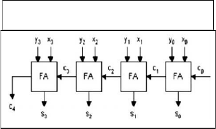
Carry look-ahead adder can produce carries faster due to parallel generation of the carry bits by using additional circuitry. This technique uses calculation of carry signals in advance, based on input signals. The result is reduced carry propagation time. For example, ripple adders are slower but use the least energy.
Carry Look-Ahead Adder
multipliers have moderate performance in speed and area.
Let Gi is the carry generate function and Pi be the carry propagate function. Then we can rewrite the carry function as follows:
Gi = Ai·Bi | ...(1) |
Pi = (Ai xor Bi) | ...(2) |
Si = Pi xor Ci | ...(3) |
Ci + l = Gi + Pi·Ci | ...(4) |
IJSER © 2015 http://www.ijser.org
International Journal of Scientific & Engineering Research, Volume 6, Issue 3, March-2015 325
ISSN 2229-5518
Thus, for 4-bit adder, we can compute the carry for all the stages as shown below:
C1 = GO + PO·CO ...(5)
C2 = G1 + P1·C1 = G1 + P1·GO +P1·PO·CO ...(6) C3 = G2 + P2·C2 = G2 + P2·G1 +P2·P1·GO + P2·P1·PO·CO ...(7) C4 = G3 + P3·C3 = G3 + P3·G2 + P3·P2· G1 + P3·P2·P1·GO + P3·P2·P1·PO·CO ...(8) In general, we can write:
The sum function:
SUMi – Ai xor Bi xor Ci – Pi xor Ci ...(9) The carry function:
Ci + l = Gi + Pi .Ci ...(10) In general, we can write the algorithm as:
If Carry in = 1, then the sum and carry out are given by,
Sum(i) = a(i) xor b(i) xor ‘1’ ...(11)
Carry(i + 1) = (a(i) and b(i)) or (b(i) or a(i)) ...(12)
If Carry in = 0, then the sum and carry out are given by,
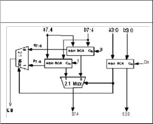
hierarchical techniques. In CSLA both sum and carry bits are calculated for two alternatives Cin = O and 1. Once Cin is delivered, the correct computation is chosen using a mux to produce the desired output. Instead of waiting for Cin to calculate the sum, the sum is correctly output as soon as Cin gets there. The time taken to compute the sum is then avoided which results in good improvement in speed.
Carry Select Adder
Sum(i) = a(i) xor b(i) ..(13)
Carry(i + 1) = (a(i) and b(i)) The sum function:
Si = CiSi0 – CiSi1
The carry function:
Ci-1 = CiCi+10 + CiCi-11
D. MULTIPLICATI
...(14)
...(15)
...(16)
ITHM
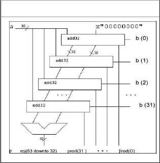
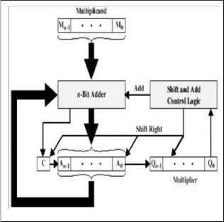
B. MULTIPLTER FOR UNSIGNED DATA Multiplication involves the generation of partial products, one for each digit in the multiplier, These partial products are then summed to produce the final product. The multiplication of two n-bit binary integers results in a product of up to 2 n bits in length.
A Partial Schematic of the Multiplier
ON ALGOR
Let the product register size be 64 bits. Let the multiplicand registers size be 32 bits. Store the multiplier in the least significant half of the product register. Clear the most significant half of the product register.
Repeat the following steps for 32 times:
• If the least significant bit of the product register is “1” then add the multiplicand to the most significant half of the product register.
• Shift the content of the product register one bit to the right (ignore the shifted-out bit).

• Shift-in the carry bit into the most significant bit of the product register. Figure 6 shows a block diagram for such a multiplier.
Multiplier of Two n-bit Values
C. CARRY SELECTADDER
The concept of CSLA is to compute alternative results in parallel and subsequently selecting the correct result with single or multiple stage
IJSER © 2015 http://www.ijser.org
International Journal of Scientific & Engineering Research, Volume 6, Issue 3, March-2015 326
ISSN 2229-5518
WALLACE TREE MULTIPLICATION METHOD
E. WALLACE TREE ADDER
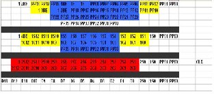
Wallace tree has been used in this project in order to accelerate multiplication by compressing the number of partial products. This design is done using half adders; Carry save adders and the Carry Look Ahead adders to speed up the multiplication. As shown in the figure below, since there are four sign extension values generated namely sign 1E,
2E, 3E and 4E for the partial product PP1, PP2, PP3 and PP4 respectively. The arrangement of total four partial product s is shown in the figure below. The second partial product had to be shifted left by two bits before adding to the first partial product. Hence the third will be shifted left by four whereas for fourth it will be shifted left by six. Hence after proper arrangement all the four partial products will be added along with the sign extension.
PARTIAL PRODUCT INITIAL ARRANGEMENT
First of all, the partial product initial arrangement is rearranged into first stage as shown in figure above. It can be seen like a tree shape here. The stage from PP36 till 1 from the 4th partial product is
moved to the first row and 3BE together with 1 is
moved up to the row partial product 2. After rearrangement, the first three rows will be added using half adder and carry save adders. The fourth partial product will not be added first but will be sent directly to the second stage. Hence, there total up to nine carry save adders and four half adders. For second stage, the summation of the first half adders in right hand side of the first stage is examined. After the summation is done to add up PP02 and PP10, The SUM (1S0) will be generated in the same column as the second stage shows where as the CARRY (1C0) will be shift left into next level of summation. In this stage, the bit PP30-PP35 is finally being added using carry save adder. At this stage, bit 4BE is also being added by using half adders. Hence, there are total six carry save adders and seven half adders needed in this stage.In third stage, it is a final stage adder and since there are only remaining two inputs to be added instead of three, thus carry look ahead is used to perform the final summation based on the Sum and Cout signal in which had been propagated by the second stage. 13-bit carry look ahead had been designed to be used in this Wallace tree final stage. The bit PP00 and PP01 are directly sent to the output without going through any gate level. Hence, Wallace tree adder will have a
17 bit length output including the carry from the final bit.
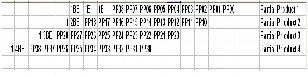
F.BOOTH MULTIPLIER BY AN EXAMPLE
Let us see an example demonstrating the whole procedure of Booth multiplier (Radix -4) using Wallace Tree and Sign Extension Correctors.Let us take Example of calculation of (34×-42).
Multiplicand A = 34 = 00100010
Multiplier B = -42 = 11010110 (2’s Complement form)
A×B = 34 × -42 = -1428
First of all, the multiplier had to be converted into radix number as in Figure below. The first partial product determined by three digits LSB of multiplier that are B1, B0 and one appended zero. This 3 digit
IJSER © 2015 http://www.ijser.org
International Journal of Scientific & Engineering Research, Volume 6, Issue 3, March-2015 327
ISSN 2229-5518
number is 100 which mean the multiplicand A has to multiply by -2.To multiply by -2, the process takes two’s complement of the multiplicand value and then shift left one bit of that product. Hence, the first partial product is 110111100. All of the partial products will have nine bits length. Next, the second partial product is determined by bits B3, B2, B1 which indicated have to multiply by 2. Multiply by 2 means the multiplicand value has to shift left one bit. So, the second partial product is
001000100. The third partial product is determined by bits B5, B4, B3 in which indicated have to multiply by 1. So, the third partial product is the multiplicand value namely 000100010. The forth partial product is determined by bits B7, B6, B5 which indicated have to multiply by -1. Multiply by -1 means the multiplicand has to convert to two’s complement value. So, the forth partial product is
111011110. Figure below shows the arrangement
for all four partial products to be added using Wallace tree adder method. 1E, 1BE 2E, 3E and 4E is obtained based on the Table 4.2. The way on how this sign E is arranged has been shown in Wallace Tree Multiplication Method above. The Wallace tree for the Example is given below.
Method showing How Partial Products Should Be
Added
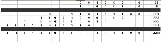
To prove the output result is correct:
11111101001101100 =
20(0) + 21(0) + 22(1) + 23(1) + 24(0) +
25(1) + 26(1) + 27(0)
+ 29(1) + 210(0) + 211(-1) = 4 + 8
+ 32 + 64 + 512 – 2048 = -1428
III. LOW POWER OPTIMIZATONS
Power optimization is the use of electronic design automation tools to reduce the power consumption of a digital design, such as that of an integrated circuit, while preserving the functionality.
A. Optimization of Multiplier recoding schemes for Low power
The multiplier operand Y is often recoded into a radix higher than 2 in order to reduce the number of partial products. The most common recoding with digit set {-2, -1, 0, 1, 2}. For a series of consecutive
1’s, the recoding algorithm converts them 0’s surrounded by a 1 and a (-1), which has potential of reducing switching activity. At the binary level, there are many design possibilities. The traditional design objectives are small delay and small area. The power issues of different designs have not been addressed well.Radix-4 multipliers could consume
less power than their radix- 2 counterparts as recoding reduce the number of PPs to half. However, the extra recoding logic and the more complex PP generation logic may present significant overheads. In addition, recoding introduces extra unbalanced signal propagation paths because of the additional delay on the paths from operand Y to the product output. We have showed that Wallace tree multipliers consumed less power than Booth-recoded radix-4 multipliers although the radix-2 scheme had twice as many PPs as the radix-4 scheme. This leads us to believe that the design of recorders and PP generators plays an important role in the overall power consumption in multipliers.
B. High level Comparison
When we go for high level comparisons we have two parameters for us when we consider different types of recoding schemes. It is the recoder and the partial product generator. The delay of REC and PPG isestimated roughly as equivalent XOR2 gate delay (TXOR2) without considering fan-out and signal transition directions. Simple gates such as AND2 have the delay of 0.5TXOR2. Two-level AND/OR gates and MUX21 have the same delay as XOR2.Among above recoding schemes, THREE_SIGNAL_1 has both the simplest recoder and the simplest PP generator. But doesn’t have a unique zero handling. After analyzing it was found out that in an m × n bit radix-4 multiplier, the total area of recoders is n/2AREC1b while the total area of PP generators is n /2 * (m+1)APPG1b , where AREC1b is area of 1-bit recoder cell area and APPG1b is area of 1-bit partial product generator cell area.
Hence since partial product generators (PPG) occupy larger areas than the recoders, we need to simplify PP generators for power saving.
In addition,unique zero handling is desired in order to reduce the number of unnecessary switching activities.
IV. OUTPUT WAVEFORMS
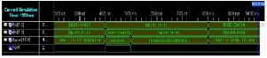
BOOTH MULTIPLIER OUTPUT
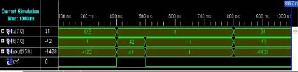
Binary Form output
Signed Form Output
WALLACE TREE MULTIPLIER OUTPUT
IJSER © 2015 http://www.ijser.org
International Journal of Scientific & Engineering Research, Volume 6, Issue 3, March-2015 328
ISSN 2229-5518
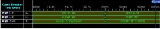
Binary Form Output
Signed Form Output
V. CONCLUSION AND FUTURE WORK
After all this then we tried to improve power efficiency of circuits. Hence we went for studying different recoding schemes along with their Partial Product generators and study time and power required by them in a multiplication process. After studying them we went to modify one of the recoding schemes to find a proper combination of recoder and PP generator such that we will have simplest PP generator as these take maximum area in a cell area and then take care of zero handling as it handles most of the switching activities. Hence we ended up creating a better recoding scheme.As an attempt to develop arithmetic algorithm and architecture level optimization techniques for low-power multiplier design, the research presented in this dissertation has achieved good results and demonstrated the efficiency of high level optimization techniques. However, there are limitations in our work and several future research directions are possible. One possible direction is radix higher-than-4 recoding. We have only considered radix-4 recoding as it is a simple and popular choice. Higher-radix recoding further reduces the number of PPs and thus has the potential of power saving. Another possible direction can be representation of Arguments such as in sign- magnitude or 2’s compliment form which in any case would prove better according to situation and require less power and consume less time.
REFERENCES
1. Armstrong J R and Gray F G (2000), VHDL Design Representation and Synthesis, 2nd Edition, Prentice Hall, USA, ISBN: 0-13-021670-4.
2. Asadi P and Navi K (2007), “A Novel Highs- Speed 54-54 Bit Multiplier”, Am. J.
3. Brown S and Vranesic Z (2005),
Fundamentals of Digital Logic with VHDL Design,
2nd Edition, McGraw-Hill Higher Education, USA, ISBN: 0072499389.
4. Hasan Krad and Aws Yousi (2010), “Design and Implementation of a Fast Unsigned 32-bit
Multiplier Using VHDL”.
5. Meier P C H, Rutenbar R A and Carley L R (1996), “Exploring Multiplier Architecture and Layout for Low Power”, CIC’96.
6. Navabi Z (2007), VHDL Modular Design and Synthesis of Cores and Systems, 3rd Edition, McGraw-Hill Professional,USA,ISBN:
9780071508926.
7. Sertbas A and Ozbey R S (2004), “A Performance Analysis of Classified Binary Adder Architectures and the VHDL Simulations”, J. Elect. Electron. Eng., Vol. 4, pp. 1025-1030, Istanbul, Turkey.
8. Software Simulation Package: Direct VHDL, Version 1.2 (2007), Green Mounting Computing Systems Inc.,Essex, VT, UK.
9. Stallings W (2006), “Computer Organization and Architecture Designing for Peljormance”, 71h ed., Prentice Hall, Pearson Education International, USA, ISBN: 0-13-185644-8.
10. Wakerly F (2006), Digital DesignPrinciples and Practices, 4th Edition, Pearson Prentice Hall,USA, ISBN:0131733494.
IJSER © 2015 http://www.ijser.org