International Journal of Scientific & Engineering Research, Volume 5, Issue 9, September-2014 1258
ISSN 2229-5518
Growth and memory switching effect in the quaternary thallium chalcogenide Tl2GaInTe4 semiconductor compound
Jazi Abdullah Mohammed Abdulwahed
physics Department, Umm Al-Qura University College in Qunfudah- Female-KSA
Jazi1430@windowslive.com
Abstract
High quality single crystal of the quaternary thallium chalcogenide Tl2 GaInTe4 compound were grown by a modified Bridgman technique. The goal of this paper is to present experimental results of the switching effect and analyze qualitatively the influence of various factors such as temperature, light illumination and sample thickness on switching behavior of the high quality chalcogenide semiconductor Tl2 GaInTe4. Current-controlled negative resistance of Tl2 GaInTe4 has been observed for the first time. It has been found that Tl2GaInTe4 single crystal exhibit bistable or memory switching. The switching process takes place with both polarities on the crystal and has symmetric shapes. Current-voltage characteristics of Ag-Tl2GaInTe4 -Ag structures exhibit two distinct region, high resistance OFF state and low resistance ON state having negative differential resistance. Tl2 GaInTe4 is a quaternary semiconductor exhibiting S-type I-V characteristic. The specimen under test showed threshold switching with critical field of switching 116 V/Cm at 213K.
Keywords: quaternary chalcogenide, Tl2 GaInTe4 , switching, memory, NDR region, S-shape.
1- Introduction
In the past three decades, significant interest in chalcogenide semiconductors has been shown by various workers owing to their interesting physical properties as well as their wide technological applications.(1) The ternary semiconducting chactcogenides with the
IJSER © 2014 http://www.ijser.org
International Journal of Scientific & Engineering Research, Volume 5, Issue 9, September-2014 1259
ISSN 2229-5518
formula TlBX2 where B=Ga or In and X= S, Se or Te belong to the III-III-Vl2 family and have a low – dimensional layered or chain structure.(2,3)TlGaTe2 and TlInTe2 have received a great deal of attention due to their optical and electrical properties in view of the possible optoelectronic device application.(4,5)
Quaternary thallium chalcogenide Tl2 GaInTe4 is formed from TlGaTe2 - TlInTe2 system having the ratio 1-1. The quaternary Tl2 GaInTe4 crystal belongs to the new group of chain structure, has a band gap of 0.88 eV.
Electrical threshold switching and memory in semiconductor have a roused great interest in recent years. Among the materials in which these effects takes place there are chalcogenides. Some of the ternary and quaternary compounds are known to have nonlinear current- voltage (I-V) characteristics and switch from the high resistance ((OFF)) state for lower applied voltages, to the low resistance ((ON)) state for higher voltages.(6,7) Therefore some of these compounds can be used as micro switches in electronic circuits to switch current passing through the circuit ((ON)) or ((OFF)) at the points of the circuit where they are incorporated. It is well known that the negative differential resistance (NDR) device can be used in many applications(8), to create extremely fast and compact circuits. Hence researchers are trying to discover new materials and compounds which can be used for operation as bistable devices. The quaternary thallium chalcogenide Tl2 GaInTe4 belong to the new group semiconductor exhibiting S-type I-V characteristics. The present authors have investigated the electrical conductivity and Hall coefficient.(9) Also the thermoelectric properties of this compound was studied and reported. (10) previously by the same authors. In view of the absence of publication of these phenomena in this compound and also in view of recent interest in this group of compound, the author undertook such work and reports here his investigation of switching effect and some factors affecting it . The electrical switching phenomena have, from the beginning, attracted
considerable interest, and have been investigated by many authors.
IJSER © 2014 http://www.ijser.org
International Journal of Scientific & Engineering Research, Volume 5, Issue 9, September-2014 1260
ISSN 2229-5518
A lot of work has been done to establish the mechanism of switching process,(11,12) but at present there still exists some uncertainty about the actual physical content of these theories. Since then the characterization and utilization of this negative-resistance behavior has received considerable attention. The aim of this work is to study the switching phenomenon in Tl2GaInTe4 single crystal in wide range of temperatures as well as light intensity and sample thickness. The absence of data on the characteristics switching about this compound makes it difficult to estimate potential application of this material in electronic technology.
2- Experimental procedures
2-1- Sample preparation
The modified Bridgman technique was used to grow Tl2 GaInTe4 single crystal from astoichiometric melt of the initial materials sealed in evacuated (~10-6 Torr ) quartz ampoules each with a tip at the bottom. All the initial materials used were extra pure elements (99.9999%). The appropriate amounts were first sealed in evacuated quartz ampoule. Tl2GaInTe4 single crystals were grown from TlGaTe2 and TlInTe2 polycrystalline by slight freezing of the charge in sealed evacuated quartz ampoule. The tipped silica tube was internally coated with aspecular layer of pyrocarbon before introducting the chemicals. In the first procedure the tube was placed in a three-stage tube furnace in which controlled temperature gradient was maintained. The ampoule is allowed to move with a constant rate of
1.5 mm/h through the stationary furnace. The details of the experimental apparatus and method of growth technique was described and reported elsewhere.(13)
The movement of the ampoule was very gently and slowly with the aid of the hydraulic mechanical system. At least two weeks growth are need to obtain Tl2GaInTe4 single crystal.(9) The resulting ingots (grey-black in color) showed a good optical quality and had no cracks or voids on the surfaces. The single crystallinity of this material was verified by means of x-ray diffraction (XRD) technique. The samples for measurement were taken from the middle of ingots with a razor
IJSER © 2014 http://www.ijser.org
International Journal of Scientific & Engineering Research, Volume 5, Issue 9, September-2014 1261
ISSN 2229-5518
blade. All samples of Tl2GaInTe4 used in the present study were freshly cleaved from a crystal grown in the same ampoule.
2-2-Switching –effect measurements
Specimens of Tl2GaInTe4 with plane-parallel mirror surfaces were prepared from a large ingot. Their typical dimensions are
4.2x3.2x1 mm3. The samples are symmetric sandwich type structure
in which single crystals are placed between two metal electrodes. The sample holder was described early.(14) The system was attached to a vacuum pump giving the possibility of measurements under vacuum. The environment temperature of the specimens under test was measured by means of a calibrated spot-welded chromel-alumel thermocouple. The investigation was carried in wide range of temperature to demonstrate the influence of the ambient temperature on the switching behavior of the crystal. The current- voltage characteristic was measured using programmable power supply thermo EC-type. The current was measured by means of digital keithley 617 electrometer. The current passing through the sample can be easily reversed or cut-off by applying three-pole doule stage reversing switch. In order to investigate the effect of light intensity on the switching phenomena at 193 k, samples with appropriate thickness were mounted in a cryostat equipped with suitable windows and clamped in its holder provided with aperture to allow the passage of the radiation. Details of the apparatus and
cryostat as well as the utilized circuit are described in reference.(15)
The sample was illuminated at normal incidence. Luxameter (Fisher Scientific mark) was used for measuring light intensity. The current and the potential drop across the sample as a function of intensity of illumination were registered directly. The effect of sample thickness on CVC was also studied. A specimen with an initial thickness equal to
1mm was first tested for its current-voltage characteristics, and its thickness was then successfully reduced. Samples with thickness varying from 1mm to 0.2 mm were used to investigate the influence of the sample thickness on the switching characteristics.
3- Results and discussion
IJSER © 2014 http://www.ijser.org
International Journal of Scientific & Engineering Research, Volume 5, Issue 9, September-2014 1262
ISSN 2229-5518
In the present investigation, I studied the switching phenomenon of the quaternary thallium chalcogenide, in a sandwich type Ag- Tl2 GaInTe4 structure. This phenomenon was observed when the current-voltage characteristics were measured as a function of the increasing applied electric field. The effects of the temperature, the light intensity, and the sample thickness on the switching behavior were observed.
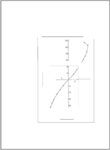
3-1- CCNR (current-controlled negative resistance) with memory. Fig.1 shows the I-V characteristic of Tl 2GaInTe4 single crystal under DC condition at T =213°k. At low applied voltages the characteristic in ohmic and the sample has a high resistivity [ 102 Ω cm ]. It becomes linear with a slope of about 2 at higher values of the voltage until the current rises steeply .Afterwards the sample goes into a state of lower resistance . This state is maintained even without any energy being applied to the sample. A current pulse of about 2.1 mA amplitude can bring the sample to its original state of high resistance . The threshold voltages for the passage from the high to the low resistance state in this sample whose thickness is about 1mm, are of about 11.6V .The I-V characteristic reported in fig1 where it can be seen that the process takes place with both polarities on the crystal and has symmetrical shape with respect to the reversal of the applied voltage and current In the highly resistive state, the material is ohmic at field below 116 V/Cm.
When the applied voltage exceeds some critical values of potential Vth the unit switches along the load line to the conduction state. As the crystal goes into the conduction state it remains there, even if it is taken away from the circuit. A highly conducting state is retained in the absence of a voltage for an indefinite time, which is important in data storage. The process can be repeated several times. The memory switching phenomenon is an effect which follows a negative-resistance process. The form of the I-V characteristic suggests that the
memory effect is composed of two processes.
IJSER © 2014 http://www.ijser.org
International Journal of Scientific & Engineering Research, Volume 5, Issue 9, September-2014
ISSN 2229-5518
1263
e
I
..'..,._ IO
a
Fig( I) Current-voltage characteristic for TI2GainTe4 single crystal during switching process with both polarity.
IJSER ©2014 h!lp'/lwww.ijser.org
International Journal of Scientific & Engineering Research, Volume 5, Issue 9, September-2014 1264
ISSN 2229-5518
(1) One is an electronic process which brings the sample into an S-type negative resistance zone. This process seems to be due to a double injection phenomenon.(16)
(2) The other one could be a thermal effect which is caused by the current previously canalized in the filament. There well be a Joul heating effect in the filment due to the high current in the device and the temperature rise so produced is sufficient to form the mono-state ON-state. In order to explain the ON-state switching can be included by (a) a sharp increase in carriers concentration (b) a sharp increase in mobility, or (c) sharp increase in both.
It was found that the reversing of the voltage applied on the sample resulted to the same behavior, indicating that the silver paste formed an ohmic contact with the investigated sample. The parameters of the high- resistivity, low-resistivity state depend to some extent on the quality of the sample (its thickness) and on the surrounding condition (temperature, illumination).
3-2-Temperature dependence of switching phenomena.
The I-V characteristics are strongly influenced by ambient temperature as shown in fig 2. In the temperature range of investigation (133-223)k, the characteristics shape is the same as in fig 1 with an increase in temperature the current-voltage characteristic as a whole is shifted toward the lower potentials. The temperature dependence of the I-V characteristic is an important for information storage applications. Usually, in memory switching materials different samples of the same thickness are used to study the effect of temperature on the switching behavior. As seen from these curves for the I-V behaviors there are two distinct regions, one is the OFF state region and the other negative differential resistance (NDR region). As is evident from the experimental curves as well as
predicted by the electrothermal model.(17,18) The ambient
temperature greatly influences both the form of the CVC
curves and the threshold voltage V th, and holding voltage V h.
IJSER © 2014 http://www.ijser.org
l.{)

;:!!
E
--- --- --
0".'.
' ·.. \ '• "
•, "·\ •,
1'1 tbl\
cr.:-
".;:,'l
ot•
•1!1'\' \ \ ..,, ••••• '•,,.
. .'\lJ'-\:\ \ ',.··., '•..,,., '•,,'•,,
A i ll 14
"tUf(
' lliAr'
11ltK
. 'ilii"
n 193 K
..0
"E'
J \', \ •, '•, •,
' \ \ ·., '.
X ' .. '• •, •,
'Wilt
Jl'ili
.. llllll
...I
;:l
0
>
-.5...
".,'
...
•I \ \ '• '•, '•,
\ '•,, ..., '•,,
I.
o ai
N V>
ffi
"' "..'
bO - "'"=
/ :::-·-:-!-:-:---.
-:---:_..- ;,
c
;:::
"'
- ........_._- =--==--- - ··--
;> -•..
6'o
Ji
Fig (2) C urrent-voltage characterist ics for TI2GalnTe4 single crystal at various temperatures.
u
<;:::
'-
0
(ij
c
....
;:l
0 0...0...
-l.{) "c'l.{.)
0 0'>
· C'J
-Ol C'J
zE :z:
.fU'l
International Journal of Scientific & Engineering Research, Volume 5, Issue 9, September-2014 1266
ISSN 2229-5518
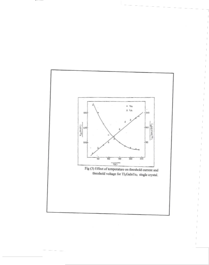
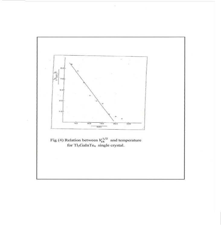
The NDR region of the curves is more pronounced at lower ambient temperature. The transition from the low to the high conductivity state of the curves is almost abrupt at lower temperature. The threshold voltage Vth after which the NDR region set in, become higher with decreasing temperature. There exist some fluctuations in the value of Vth when the first three or four switching cycles were measured. After three or four sets of measurements, the device become more stable and Vth sets to a constant value. Also we observe from the curves in fig 2 the conduction state can be kept at a certain holding current In and holding voltage Vh. The holding voltage Vh increase with temperature, while the holding current Ih is independent on temperature and has the same value at the whole temperature range of investigation. Also it is found that the threshold and memory switching stability increase with temperature increase. As the temperature increases one can observe three zones in the characteristics, ohmic zone, at low voltage, non-ohmic at higher voltages and thirdly the threshold voltage Vth. From the curves in fig.2 we notice the range of measurements begins from 133 to 223 k, since at temperature in excess of 223 k the OFF device with increasing field applied eventually exhibits filamentary breakdown and double injection, the enhanced conducting state being lost if a certain minimum voltage is not maintained. The effect of the ambient temperature on the switching parameters Vth and Ith is illustrated in fig.3. It is clear from the figure that cooling increases the threshold voltage where as the threshold current decreases, i.e as the temperature increases the threshold voltage decreases and the threshold current increases. This indicates that an electrothermal mechanism is involved in the switching process. The dependence of Vth on T was analyzed on the basic of the thermal- field Frenkel effect. Allowance for this effect in reference(19) yields the following expression
relating Vth and T.
𝜋𝜖0 𝜖∞𝑑 2
![]()
𝑉𝑡ℎ = �
� (𝑄 − 𝑐𝑇)
𝑒
IJSER © 2014 http://www.ijser.org
International Journal of Scientific & Engineering Research, Volume 5, Issue 9, September-2014 1267
ISSN 2229-5518
International Journal of Scientific & Engineering Research, Volume 5, Issue 9, September-2014 1268
ISSN 2229-5518
Where 𝜖0 is the permittivity of vacuum, 𝜖∞ is the
electron component of the permittivity, d is the
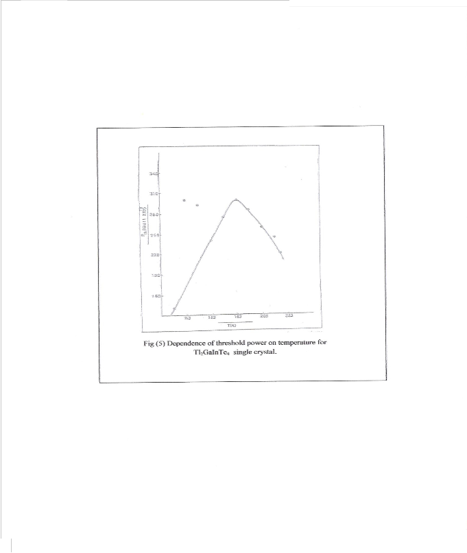
distance between the electrodes, c is a constant, e is the electron charge, Q is the depth of the potential well and T is the absolute temperature. Variation of Vth with temperature is plotted in fig.4. On the basis of the equation, using the coordinates (Vth )1/2 and T. Clearly, within the limits of the experimental error the results fit a single line. It is seen that in the whole temperature range of investigation, the threshold voltage decreases with temperature increases as expected from the above equation. This shows that the switching in Ag-Tl2GaInTe4-Ag structures from a high to a low resistivity state occurs under the simultaneous action of an electric field and temperature.(20) This is supported by the dependence of the threshold field on thickness of the active region. The power necessary to
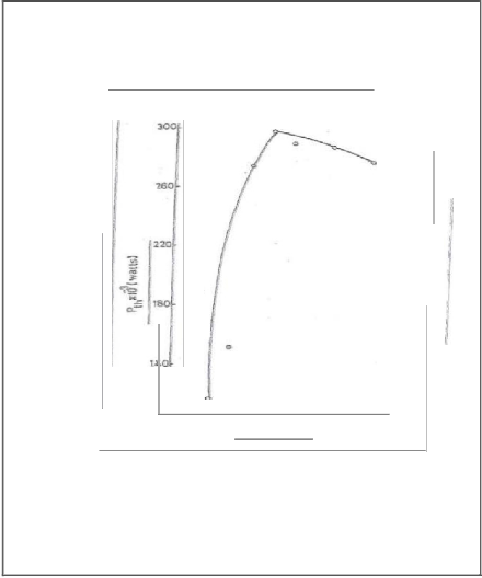
change the material from the high- resistance state to the low- resistance state called threshold power (Pth). The threshold power dependents also on the ambient temperature. The dependence of the threshold power on temperature was plotted in fig.5. It is found that the relation between the threshold power and temperature increases exponentially with temperature up to 183 k, after which the threshold power decreases exponentially with temperature. This led us to the assumption that as the temperature increases the rate of thermal generation of free charge carriers greater than the rate of recombination and the effect of trapping centers can be neglected, this led to increase
of the threshold power as the temperature increase up
IJSER © 2014 http://www.ijser.org
International Journal of Scientific & Engineering Research, Volume 5, Issue 9, September-2014 1269
ISSN 2229-5518
IJSER © 2014 http://www.ijser.org
International Journal of Scientific & Engineering Research, Volume 5, Issue 9, September-2014 1270
ISSN 2229-5518
IJSER © 2014 http://www.ijser.org
International Journal of Scientific & Engineering Research, Volume 5, Issue 9, September-2014 1271
ISSN 2229-5518
to 183 k. After which the effect of recombination
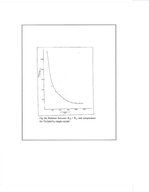
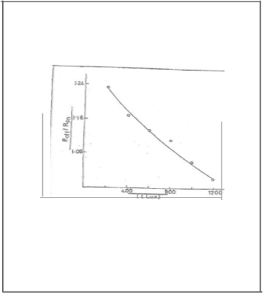
become more than the generation also the effect of trapping centers increases, all these factors led to the decrease of the threshold power as the temperature increase, in the high temperature region (183-223k) this result is quite logical, since the power necessary to initiate switching decreases when temperature increases. The effect of surrounding temperature on the sample resistance ratio (ROFF /RON) as seen in fig.6 depends on temperature which decreases exponentially with temperature. The resistance ratio ROFF/RON varies from 11.4 to 1.036 in the range of temperature investigated.
3-3- Influence of light intensity on switching effect.
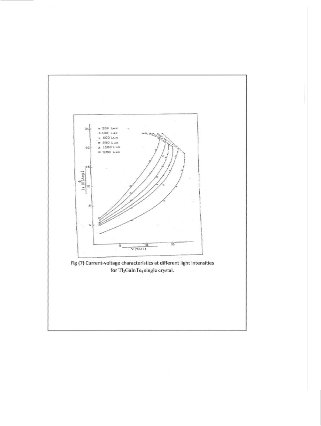
The VAC of Tl2 GaInTe4 , when the sample illuminated with different does of white light extended from 200 up to 1200
Lux, is illustrated in fig.7. The measurements were taken at low temperature and under vacuum, to prevent condensation around the cryostat which delays the incident light on the sample. The measurements were taken at T=193 k. As shown from the figure the curves of the CVC under illumination has the general form of switching with S-shape. It is evident from this figure that I-V characteristics as a whole are shifted toward lower potentials with an increase in the intensity of the incident light, also we can see that the form of CVC and the magnitude of the photocurrent depend strongly on the intensity of the incident light. This means that in case of weak illumination the threshold voltage is larger and the threshold current value smaller than the value obtained in case of intense light. The characteristic behavior can be described as follows (a) values of high resistance state decrease by increasing light intensity (b). The field necessary for switching
to be performed is reached early on increasing the light
IJSER © 2014 http://www.ijser.org
International Journal of Scientific & Engineering Research, Volume 5, Issue 9, September-2014 1272
ISSN 2229-5518
IJSER © 2014 http://www.ijser.org
International Journal of Scientific & Engineering Research, Volume 5, Issue 9, September-2014 1273
ISSN 2229-5518
IJSER © 2014 http://www.ijser.org
International Journal of Scientific & Engineering Research, Volume 5, Issue 9, September-2014 1274
ISSN 2229-5518
intensity dose (c). Near switching delicate control of the applied voltage is required since an increment of 0.1 volt is sufficient to move the sample from a stationary condition to a switching condition, d-The holding voltage Vh decreases as the intensity of illumination increases, while the holding current Ih does not vary with the intensity of illumination.
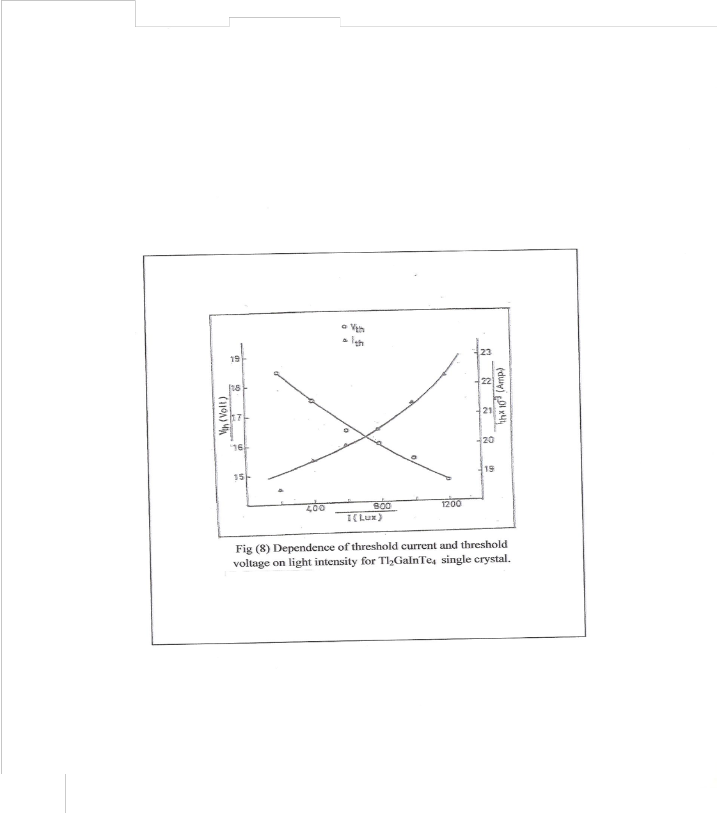
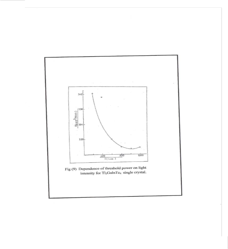
The variation of the threshold voltage and current with light intensity is represented in fig.8. As can be seen, threshold voltage decreases with light intensity, whereas the threshold current increase with light illumination, both of them vary with exponential relation. The main contribution comes from photo carriers generation through excitation states and is larger than recombination process. The relation between threshold power and light intensity is represented graphically in fig.9. As it is noticed Pth decreases exponentially with increasing incident light intensity.
This may be photogeneration process for excited free charge carriers, which take place under illumination of the sample, leading to a small power required for switching as the illumination dose increase. The dependence of the ratio ROFF/R ON on the illumination intensity is shown in fig.10,where it is obvious that this ratio decreases continuously with illumation intensity increases. The ratio ROFF/R ON varies from
1.37 to 1.01 in the range of light intensity.
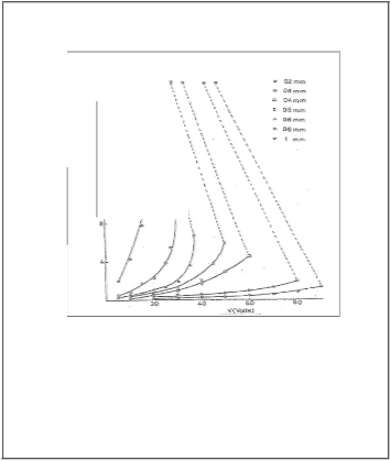
3-4- Effect of sample thickness
The overall feature of I-V characteristic of Tl2 GaInTe4 are altered by change in sample thickness. For switching process one has to choose a specimen whose resistance is changed from high value (OFF state) to a very low value (ON state) by the lowest switching power. This can be achieved through the study of the effect of the specimen thickness on switching. The measurements were taken in the dark, under vacuum at temperature T=183 k. Fig.11 represents the dependence of the
switching behavior on the thickness of Tl2 GaInTe4 specimen.
IJSER © 2014 http://www.ijser.org
International Journal of Scientific & Engineering Research, Volume 5, Issue 9, September-2014 1275
ISSN 2229-5518
IJSER © 2014 http://www.ijser.org
International Journal of Scientific & Engineering Research, Volume 5, Issue 9, September-2014 1276
ISSN 2229-5518
IJSER © 2014 http://www.ijser.org
Internatio nal jo urnal of Scientif ic & Engineering Research, Volume 5, Issue 9, Se ptember-2014
155N 2229-5518 1277
I
Fig (1 O) Relation between R..tr I R..n and light intensity for
TI2GainTc4 single crystal.
IJSER © 2014
http:llwww.ijser org
International Journal of Scientific & Engineering Research, Volume 5, Issue 9, Septernber-2014
ISSN 2229-5518 1278
I
l- l l
....0.
\ \
'.'
\ \
\
' ' '
\ ·.
I <
\.
'
'
Fig (11) Current-voltage characteristics at different values of sample thickness for ThGalnTe4 single crystal.
IJSER © 2014 httpJfwwwJiser.ora
International Journal of Scientific & Engineering Research, Volume 5, Issue 9, September-2014 1279
ISSN 2229-5518
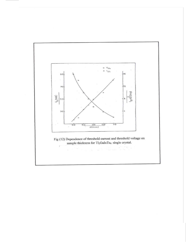
The investigated range of the sample thickness varies from 1 mm to 0.2 mm. The figure indicates that the threshold potential and current change with the inter electrode gap and the width of the dashed lines which represents the variation from OFF to ON state decreases with thickness. This result indicates that the switching can be easily controlled with the sample thickness. The holding voltage also affected with the active thickness of the specimen (increases with the decrease of sample thickness) and its value lies between (12-32) volt, whereas holding current Ih is independent on the sample thickness and has the value 22.8 mA. The variation of the threshold voltage and current with thickness is represented in fig.12. It shows that Vth decreases exponentially as the crystal thickness increases, whereas Ith decreases linearly as the active region between the electrodes decreases. This indicates that the switching behavior can be easily controlled with specimen thickness. The dependence of Vth on thickness shows that switching is a bulk effect. The previous assumption that switching occurs under the simultaneous action of the electric field and temperature is supported by the dependence of the threshold field on the thickness of the active region. Fig.13 shows the dependence of the threshold field on the thickness of the Tl2 GaInTe4 samples. The experimental results indicate that the dependence exponentially decreases as the sample thickness increases as shown in fig.13. This is due to the appearance of Pool-Frenkel conductivity in the thinner samples, which occurs for fields greater than about
200 V/Cm(20). It is clear that Eth decrease as the sample
thickness increase. This indicates that the electric field has a profound influence on the ability of the samples to undergo a transition from the OFF state to an effective region of NDR. This supports the suggestion that the mechanism of the switching in Tl2 GaInTe4 sample may involve both electric and
thermal processes.(21) Investigation of the effect of the sample
thickness on switching phenomena is useful for a chosen
IJSER © 2014 http://www.ijser.org
International Journal of Scientific & Engineering Research, Volume 5, Issue 9, September-2014 1280
ISSN 2229-5518
IJSER © 2014 http://www.ijser.org
Interna tional Journal of Scientific & Engineering Research, Volume 5, Issue 9, Septernber-2014
ISSN 2229-5518
t]·
t&
sao
40
Fig (13) Relation between threshold field and
sample thickness for ThGainTe4 single crystal.
1281
International Journal of Scientific & Engineering Research, Volume 5, Issue 9, September-2014 1282
ISSN 2229-5518
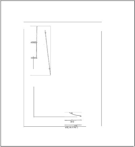
specimen whose resistance is changed from high value (OFF state) to a very low value (ON state) by lowest switching power. The variation of the threshold power Pth with sample thickness was plotted in fig.14. It is clear that the threshold power increases sharply with sample thickness increase and reaches its maximum value at d=0.5 mm, then it decreases with the increase of sample thickness. The relation between ROFF/R ON and sample thickness of Tl2GaInTe4 single crystal is shown in fig.15. It is clear from the figure that the ratio is strongly dependent on sample thickness. Increasing ((d)) leads to larger value of ROFF /RON . The resistance ratio ROFF /RON varies from 1.62 to 17.54 in the range of sample thickness under investigation
4- Conclusion
The major features of the switching in Tl2GaInTe4 single crystal can be summarized as follows:
∗ From the I-V characteristic we can see that the process take
place with both polarities on the crystal and has symmetrical shape.
∗ When the applied voltage exceeds threshold the unit
switches along the load line to the conducted state. The critical field for switching in Tl2 GaInTe4 is 116 V/Cm at
213k.
∗ The specimen under test exhibit bistable or memory
switching of the negative resistance process.
∗ The VAC has S-shape type from the common form of the
switching phenomena with CCNR effect.
∗ The switching phenomenon in our sample is very sensitive
to the temperature, intensity of light and sample thickness.
∗ The switching parameters (Vth, I th, Pth, Eth, Vh, Ih, ROFF /RON )
are checked under the influence of different factors of the ambient conditions.
∗ The parameters of the high-resistivity, low-resistivity state
depends to some extent on the quality of the sample and
on the surrounding conditions.
IJSER © 2014 http://www.ijser.org
Internatio nal jo ur nal of Scientific & Enginee rin g Research, Volu me 5, Issue 9, Se pte m be r- 2014
ISSN 2229-5518 1283
o..tt. o.o o.a
d:(tnm)
Fig (14) Dependence of threshold power on sample
thickness for TlzGalnTt!4 single crystal.
Inte rnatio nal journal of Scie ntific & En ginee rin g Research, Vol u me 5, Iss ue 9, Se pte mbe r- 2014
ISSN 2229-5518 1284
18
IG
!4
0
tt
c: 10
8
6
4
0
2
9·2 0.4 0.6 08
d(mm)
Fig (15) Relation between Rorr/ Ron and sample thickness for TI 2GalnTe4 single crystal.
USER @2014
http·llwww.l!ser.org
International Journal of Scientific & Engineering Research, Volume 5, Issue 9, September-2014
ISSN 2229-5518
1285
IJSER © 2014 http /lwww .llser.org
International Journal of Scientific & Engineering Research, Volume 5, Issue 9, September-2014 1286
ISSN 2229-5518
References
1. AL-Gamdi A.A.,Nagat,A.T.,Bahabri F.S.,AL-Orainy R.H.,AL- Garni S.E., Study of the switching phenomena of TlGaS2 single crystals, Applied surface science 257 (2011)3205-32010
2. Guler I.,Gasanly,N.M.,Trapping center parameters in TlInSSe layered single crystals by thermally stimulated currents measurements,J.alloys,and compounds 485(2009)41-45.
3. Gasanly N.M effect of temperature and isomorphic atom
substitution on optical absorption edge of TlInS2xSe2(1-x) mixed
crystals (0.25 ≤ 𝑥 ≤ 1) cryst Res. Technol.45(2011)525-528.
4. Kurbanov,M.M.(Thermalexpansion and isothermal compressibility
of TlGaTe2, Inorganic Materials 41(2005)1277-1279.
5. Gojaev, E.M.Allakhyarov, E.A.Nazarov, A.M.,Gyul Mamedov, Khalilova.D.and Mamedov, E.M.(Acoustophotovoltic effect in TlInSe2,TlInTe2 and TlGaTe2 single crystals,Inorganic Materials
43(2007)1059-1064.
6. Damordara Das,V.,Raju K.S AND Bhaskaran A(electrical conduction in ternary semiconductors Ga5Ge20 Te75 thin films J.Appl.phys.75(1995)3262-3268.
7. Orainy R.H.and Nagat, A.T.preparation and switching behavior characterization of some quaternary thallium chalcogenide compounds,Acta physica polonica A.123(2013)1111-1115.
8. Gan,K-J.,Tsai C.S.,Liang D.S.,Tu C-D, Chen Y.H. (Multiple-input NOR logic using negative differential resistance circuits implemented by standard SiGe process). Solid-state electronics
52(2008)175-178.
9. Jazi A.M.A.((Growth and transport properties of the quaternary chalcogenides Tl2GaInTe4 compouns)),Life Science J.11(2014)109-113.
10. Jazi.A.M.A.((On the preparation and thermal transport properties
of a quaternary thallium dichalcogenide Tl2GaInTe4 compounds))
J.American science 10 (2014) 98-102.
11. MansurE,MoustafaY.M.,EL-Damrowi,G.M.,EL-Maksoud,S., Doweidar H.((Memory switching of Fe2 O3-BaO-V2 O5 glasses)) physicsa B 305 (2001) 342 – 349.
IJSER © 2014 http://www.ijser.org
International Journal of Scientific & Engineering Research, Volume 5, Issue 9, September-2014 1287
ISSN 2229-5518
12. Abdel-Aziz M.M.((Memory switching of germanium tellurium amorphous semiconductor Applied surface Science 253(2006)
2059-2065.
13. Hussein S.A.,and Nagat, A.T.(( On the preparationand electrical properties of thallium selenide monocrystals)) Cryst.Res.Tech.24 (989) 283-289.
14. Nagat,A.T,Hussein SS.A.,Gameel Y.H.and Gamal G.A. ((Switchingeffect with memory in thallium sulphide single crystals)) phys.Stat.Sol.(a) 121 (1990) 201.
15. AL-Ghamdi,Hussein S.A.,and Nassary M.M.((Memory switching
in GaSe single crystals)) Mat.Sci.Res.India 2 (2004) 107.
16. Balevicus S,Cesnys A.and DeksnysA.,((Nanosecond switching in a morphous In2 Te3 films phys.stat. sol.(a) 35 (1970) 41-43.
17. ABay B., Gurbulak B.,Yildirim M.,Efeoglu H.,and Yogurteu
Y.K.((electrothermal investigation of switching phenomena in P- type TlInSe2 single crystals)) phys.stat. sol (a) 153 (1996) 145-151.
18. Boer K.Wand Ovshinsky S.R.((electrothermal initiation of an
electronic swiching mechanism in semiconductor glasses)),J. Applied phys. 41(1970) 2675-2681.
19. Aliev,S.I.,Niftiev G.,Pliev F.I and Tagiev B.G ((Switching effect
with memory in Ga2 Te3 single crystal)).Soviet phys. semicond.
13(1979)340-342.
20. Kolomiets,V.G.Lebedev,E.A.and Taksami I.A.((Thickness effect on threshold field of Te-As-GeSi glass)).Sov.phys.Semi 3(1969)
267.
21. Prakash S.,Asokan S.and Ghare D.B ((easily reversible memory switching in Ge-As-Te glasses)) J.phys.D.Appl.phys.29(1996)
2002-2008.
IJSER © 2014 http://www.ijser.org