International Journal of Scientific & Engineering Research, Volume 6, Issue 1, January-2015 163
ISSN 2229-5518
Formulation and Design of Useful Logic Gates
Using Quaternary Algebra
Sarah Nahar Chowdhury, Asif Faiyaz, Khandakar Mohammad Ishtiak
Abstract— Multivalued logic is preferable over conventional binary logic operations for speed optimization and information handling capacity. In this paper, a set of contemporary special operators using quaternary logic have been derived from basic gates. These novel special logic gates along with their corresponding equations and truth table can be implemented to function individually and in logic blocks resulting in a reduction of circuit complexity and better speed processing in integrated circuit technology.
Index Terms— BITSWAP, INWARD, multivalued logic, OUTWARD, quaternary algebra, qudit, Sum of products.
—————————— ——————————
1 INTRODUCTION
Binary logic can be professed as the pivot of controlling the embedded fundamental and digital system of modern times. Due to its easy accessibility and widespread use of logic circuits, it is extremely quintessential in terms of its ap- plications from simple circuits to complex one. Operating with binary logic seems controlling the real world with computers and that an alternative improved approach with a better usage of transmission path, storage and processing of large amount of information in digital signal processing seems impossible. Yet, the inclusion of a ‘don’t care’ operator describes the im- portance of an intermediate or neutral stage even in binary logic. In addition to the existing binary values {0,1} we need a three valued {0,1,X} operands for constructing the Karnaugh map or applying the tabular method [1],[2]. Multivalued logic system introduces new operators in addition to binary values
{0,1} as a solution to solving these intermediate stages. It is a proposed extension of the idea that n valued logic can be used instead of two logical values (i.e. true or false, logic high or low) where n>2.
Perhaps one of the most tangible immediate benefits of higher-radix approaches like quaternary logic lie in their po- tential for reduction of the wiring congestion both on-chip and between chips. Using a single conductor to transmit three or more discrete voltages or current values allows for greater information content per wire and thus results in a circuit with reduced conductors and logic gates than the binary-valued counterpart. By providing an increase in the information con- tent per wire we can subsequently decrease the interconnec- tion cost, complexity and area also. Furthermore, multivalued number systems, such as ternary and quaternary systems with a radix more than ‘2’ (p>2) are obviously expected to have larger information handling and storage capacities.
————————————————
• Sarah Nahar Chowdhury, Ahsanullah University of Science and Technology
(AUST), Bangladesh. E-mail: sarahnahar55@gmail.com
• Asif Faiyaz, Ahsanullah University of Science and Technology (AUST),
Bangladesh. E-mail: asif.faiyaz@gmail.com
• Khandakar Mohammad Ishtiak, Ahsanullah University of Science and
Technology (AUST), Bangladesh. E-mail: ishtiak.eee@aust.edu
Many complex logic systems and associated algebras are possible due to the exponentially increasing number of opera- tors with respect to the cardinality of the quaternary logic val- ues. Arithmetic logic circuits mainly based upon addition cir- cuitry can be constructed where operations on each operand can be performed simultaneously using multiple values and thus overcoming the effect of overall circuit delay which is subsequently a function of the length of inherent carry digit propagation characteristic chain.
Quaternary algebra can be used in response to the necessity of representation of intermediate values in Hardware Descrip- tion Languages (HDL) and Symbolic Trajectory Evaluation (STE) algorithm which is used for verification of errors before the circuit is designed in EDA-CAD [1]. Quaternary algebra can even be applied to optical computing for novel photonics structures through optical quaternary logic.
Although quaternary algebra is not as widespread as bina- ry and does not have all the logic gates, earlier works suggest some proposed logic gates for quaternary. In this paper, we demonstrate some new logic gates contrary to the earlier pro- posed logic operators.
2 QUATERNARY ALGEBRA
Quaternary algebra is a subsidiary of multi valued logic. While multi valued logic deals with infinite number of values as discrete variables quaternary algebra is based upon four discrete variables including the binary values. Quaternary states {0,1,2,3} with a set of operators and axioms are used to define quaternary algebra. Each of the quaternary states
{0,1,2,3} has its two bits binary equivalents 00 (absolute low),
01 (intermediate low), 10 (intermediate high) and 11 (absolute
high). Each of the quaternary bits is called ‘qudit’[1],[3], when
expressed in numbers and can also be indicated by two binary
digits ‘a1’ and ‘a0’, respectively.
They are inscribed and packed together using the following notion A={a1,a0} and the term ‘2a1 + a0’ denotes the magni- tude of the variable ‘A’ in decimal system [4]. Quaternary states are sub categorized into symmetrical and asymmetrical
IJSER © 2015 http://www.ijser.org
International Journal of Scientific & Engineering Research, Volume 6, Issue 1, January-2015 164
ISSN 2229-5518
based upon their position of bits. If the bits of the binary equivalent of quaternary states interchange their position and still the quaternary state remain unchanged then they are known as symmetrical. Absolute states (0,3) are symmetrical as the change of bits in binary equivalent does not change the corresponding quaternary value. If the alternation of position of bits changes the corresponding binary value then they are known as asymmetrical. Intermediate states (1,2) are asym- metrical as interchanging the binary equivalents changes the quaternary state 1 to 2 and vice versa [5].
In addition to the mainstream basic operators, a number of special logic gates like INWARD INVERTER, INWARD NAND, INWARD NOR, INWARD XNOR, OUTWARD IN- VERTER, OUTWARD NAND, OUTWARD NOR, OUTWARD XNOR, BINARY BITSWAP, BITSWAP AND, BITSWAP OR and BITSWAP XOR have been introduced in [3],[4] solving much more complex functions.
The mathematical definitions of special operators [5],[6] are given below:

a a
Quaternary algebra does not replace binary logic rather it
INWARD INVERTER,

a' =
.2 ; < 2
(1)
broadens the applications of binary through high storage ca-
pacity and multitasking. That is why the logic gates derived in
binary algebra are also applicable in quaternary algebra [4].
They are OR, AND, BUFFER, BASIC INVERTER, XOR, BASIC
OUTWARD INVERTER,
a + 1;

^ a + 3;

a =
a > 1
a < 2
(2)
NAND, BASIC NOR and BASIC XNOR.
a.0 ;
a > 1

~ a ;
a asymmetric
(a) (b) (c)
BINARY BITSWAP,
a =
a ; a
symmetric
(3)
(d) (e) (f)
(g) (h)
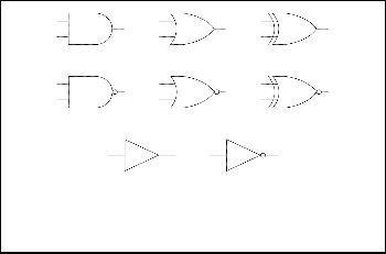
Fig. 1. Circuit symbols for the basic quaternary operators. (a) AND, (b) OR, (c) XOR, (d) BASIC NAND, (e) BASIC NOR, (f) BASIC XNOR, (g) BASIC BUFFER and (h) BASIC NOT.
TABLE 1
Basic Quaternary Multi-Input Operators Truth Table
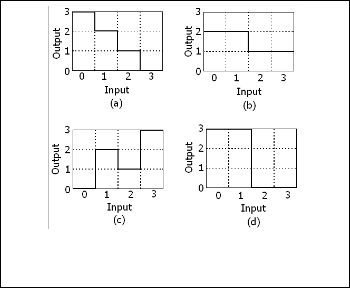
Fig. 2. Transfer functions of the quaternary inverters and inverter-like operators: (a) Basic Inverter; (b) Inward or Half Inverter; (c) Binary Bitswap; (d) Outward or Full Inverter.
Like binary logic, any function even for special logic opera- tors can be implemented in quaternary algebra using the basic SOP II form that has been proposed in [4]. Although we have multiple min terms in quaternary algebra all these min terms are primarily converted into binary equivalents and then im- plemented in the following equations.
F1 ≡a, f1 (4) F0 ≡b, f 0 (5)
where, a and b are arbitrary binary values being converted into their quaternary equivalents and then both the functions are combined to form the required SOP format to represent all the functions for logic gates [4].
F = ~ F1.2 + F0.1 (6)
IJSER © 2015 http://www.ijser.org
International Journal of Scientific & Engineering Research, Volume 6, Issue 1, January-2015 165
ISSN 2229-5518
The transformation of binary to quaternary equivalents can be done using the following transformation pairs in the truth
table.
TABLE 2
BASIC TRUTH TABLE OF SOP II FORM
~
(a)
~ (e)
~
~
(b)
~
~
(f)
~
(c)
~ (g)
~
~
(d)
~
~
(h)
~
(i)
~
~
(j)
~
(k)
~
~
(l)
Quaternary algebra can be used as models for the initial de- sign of logic circuits whether they are implemented with MVL signal levels or binary after being encoded. The most extolling part of quaternary algebra is that the interfacing of binary to quaternary and in reverse can be easily conducted using an encoder and this conversion of multi valued variables in qua-
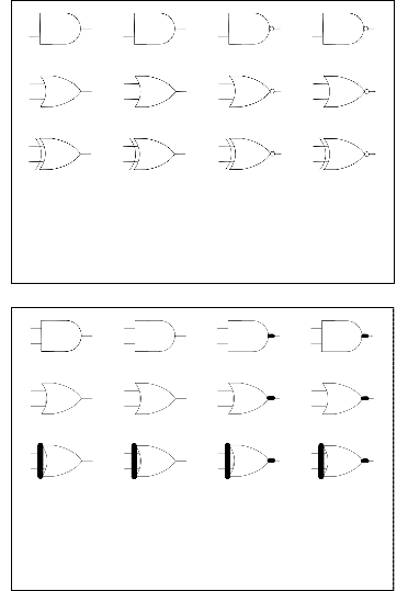
Fig. 3. Circuit symbols for the special quaternary operators and their derivatives: (a) BITSWAP AND, (b) AND BITSWAP, (c) BITSWAP NAND, (d) NAND BITSWAP, (e) BITSWAP OR, (f) OR BITSWAP, (g) BITSWAP NOR, (h) NOR BITSWAP, (i) BITSWAP XOR, (j) XOR BITSWAP, (k) BITSWAP XNOR, (f) XNOR BITSWAP.
ternary algebra to binary is called encoding. Furthermore, the conversion can also be done directly when binary system has
2m inputs and 2n outputs. The 2m inputs are grouped as m quaternary inputs and then the 2n binary outputs are convert- ed to n quaternary outputs using the transformation pair for- mat used in SOP form. Moreover, all the logic blocks of qua- ternary are compatible with binary logic design making it a paragon for dual purpose.
3 PROPOSED IDEA
◊
(a)
◊
(e)
◊
(i)
◊
◊
(b)
◊
◊
(f)
◊
◊
(j)
◊
(c)
◊
(g)
◊
(k)
◊
◊
(d)
◊
◊
(h)
◊
◊
(l)

We know in case of ordinary binary input, NAND gate can be generated combining AND operator and NOT operator. NAND gate can be implemented in two ways. One is to fabri- cate AND gate first and NOT gate subsequently. Another way is to devise it by placing NOT gate first and then AND gate. Previously only one of the orders were followed in [3]- [6] for operators like INWARD INVERTER, INWARD NAND, IN-
Fig. 4. Circuit symbols for the special quaternary operators and their
derivatives: (a) INWARD AND, (b) AND INWARD, (c) INWARD
NAND, (d) NAND INWARD, (e) INWARD OR, (f) OR INWARD, (g) INWARD NOR, (h) NOR INWARD, (i) INWARD XOR, (j) XOR IN- WARD, (k) INWARD XNOR, (f) XNOR INWARD.
WARD NOR, INWARD XNOR, OUTWARD INVERTER, OUTWARD NAND, OUTWARD NOR, OUTWARD XNOR, BINARY BITSWAP, BITSWAP AND, BITSWAP OR and BITSWAP XOR in quaternary logic like Boolean algebra. But our proposed research and data showed that when we do INWARD and then NAND, the logic table obtained is not the same as the logic table obtained when we do NAND and then INWARD. The equations derived for each corresponding or- der also shows variance in comparison to each other. Only for BITSWAP operator, the complementary equations and logic
^ (a)
^ (e)
^ (i)
^
^
(b)
^
^
(f)
^
^
(j)
^ (c)
^ (g)
^ (k)
^
^
(d)
^
^
(h)
^
^
(l)
tables of any order shows identical output. Earlier the same symbol and equation was used to demonstrate both the pro- cesses. But in our paper, we conclude our findings of different truth tables and equations for both the operations. The sym- bols used for each case has been mentioned below.
Fig. 5. Circuit symbols for the special quaternary operators and their derivatives: (a) OUTWARD AND, (b) AND OUTWARD, (c) OUT- WARD NAND, (d) NAND OUTWARD, (e) OUTWARD OR, (f) OR OUTWARD, (g) OUTWARD NOR, (h) NOR OUTWARD, (i) OUT- WARD XOR, (j) XOR OUTWARD, (k) OUTWARD XNOR, (l) XNOR OUTWARD.
IJSER © 2015 http://www.ijser.org
International Journal of Scientific & Engineering Research, Volume 6, Issue 1, January-2015 166
ISSN 2229-5518
Each logic gate can be represented by two symbols. The rea- son behind two discrete symbols used is to designate each operator having exclusive equations and logic table with a
From the K-map we get the following expression:
ba1 = a0 .b0
(9)
particular symbol. The respective equations derived are based on the SOP-II format that has been used in [4] and cannot by
Then we replace all binary variables from (9) and get (10):
any means be interchanged with each other. Let’s consider
BITSWAP AND gate and the process of deriving the specific
BA1 = (~ A. ~ B).2
(10)
equation. The quaternary truth table of BITSWAP AND gate is given below:
TABLE 3
TABLE FOR BITSWAP AND GATE.
Now, we can combine (8) and (10) to get the complete func-
tion:
BITSWAP AND (A,B) = (~ A. ~ B).1 + (~ A. ~ B).2
= (~ A. ~ B).(1 + 2)
= (~ A. ~ B).3

= (~ A. ~ B) OR
~ ( A.B)
Now, using the SOP-II format, we consider the cells which contains 1 or 3 as true for ba0 (BITSWAP AND). Similarly, we consider the cells which contain 2 or 3 as true for ba1. The re- maining cells will contain 0. The K-map for ba0 is given in the
This is the final equation of BITSWAP AND gate. Similarly, we can use the above procedure to derive the following equa- tions:
3.1 BITSWAP Operators
• BITSWAP AND, AND BITSWAP :
following table:
(~ A. ~ B) OR
~ (A.B)
TABLE 4
• BITSWAP NAND, NAND BITSWAP :
K – MAP FOR BITSWAPAND0 FUNCTION.


(~ A+ ~ B)


OR ~ (A + B)

• BITSWAP OR, OR BITSWAP :
(~ A+ ~ B)
OR ~ (A + B)
From the K-map given above, we can write the following ex- pressions:
• BITSWAP NOR, NOR BITSWAP :


(~ A. ~ B) OR ~ (A.B)
• BITSWAP XOR, XOR BITSWAP :


(~ A. ~ B+ ~ A. ~ B)
• BITSWAP XNOR, XNOR BITSWAP :
ba0 (a1 ,a0 ,b1 ,b0 ) = a1.b1
Now, we replace all binary variables from (7) and get (8):
BA0 (A,B) = (~ A. ~ B).1
Now, the K-map for ba1 is given below:
TABLE 5

K – MAP FOR BITSWAPAND1 FUNCTION.
(7)
(8)


(~ A. ~ B+ ~ A. ~ B)
The truth table shows the comparison of output of special logic gates when two basic operators are fabricated in a par- ticular order to form the special quaternary operators. From the relation we can conclude that the special operators do not follow the law of associatively and commutatively.
<a1 ,a0 > <b1 ,b0 > | 0,0 | 0,1 | 1,1 | 1,0 |
0,0 | 0 | 0 | 0 | 0 |
0,1 | 0 | 1 | 1 | 0 |
1,1 | 0 | 1 | 1 | 0 |
1,0 | 0 | 0 | 0 | 0 |
IJSER © 2015 http://www.ijser.org
International Journal of Scientific & Engineering Research, Volume 6, Issue 1, January-2015 167
ISSN 2229-5518
TABLE 6
TRUTH TABLE FOR SOME PROPOSED GATES CONTAINING

BITSWAP INVERTER.
Input Output


(~ A+ ~ B).1 + ( A + B).2


• NAND INWARD :
A B Or
Bitswap
Bitswap
Or
Nor
Bitswap
Bitswap
Nor
And
Bitswap
Bitswap
And
• INWARD OR :


(~ A+ ~ B).1 + (A + B).2
0 0 0 0 3 3 0 0
0 1 2 2 1 1 0 0
0 2 1 1 2 2 0 0
0 3 3 3 0 0 0 0
1 0 2 2 1 1 0 0
1 1 2 2 1 1 2 2
1 2 3 3 0 0 0 0
1 3 3 3 0 0 2 2
2 0 1 1 2 2 0 0
2 1 3 3 0 0 0 0
2 2 1 1 2 2 1 1
2 3 3 3 0 0 1 1
3 0 3 3 0 0 0 0
3 1 3 3 0 0 2 2
3 2 3 3 0 0 1 1
3 3 3 3 0 0 3 3
TABLE 7
TRUTH TABLE FOR SOME PROPOSED GATES CONTAINING
BITSWAP INVERTER.
3.2 INWARD Operators
• OR INWARD :

(~ A+ ~ B).1 + (A.B).2
• INWARD NOR :


(~ A. ~ B).1 + (A.B).2
• NOR INWARD :


(~ A. ~ B).1 + (A + B).2
• INWARD XOR :


(~ A. ~ B+ ~ A. ~ B).1 + ( A.B + A.B).2
• XOR INWARD :


(~ A. ~ B+ ~ A. ~ B).1 + ( A.B + A.B).2
• INWARD XNOR :


(~ A. ~ B+ ~ .A. ~ B).1 + ( A.B + A.B).2
• XNOR INWARD :


(~ A. ~ B+ ~ .A. ~ B).1 + ( A.B + A.B).2
TABLE 8
TRUTH TABLE FOR SOME PROPOSED GATES CONTAINING

INWARD INVERTER.
Input Output
• INWARD AND :

(~ A. ~ B).1 + (A.B).2
• AND INWARD :


(~ A. ~ B).1 + (A + B).2
• INWARD NAND :
IJSER © 2015 http://www.ijser.org
International Journal of Scientific & Engineering Research, Volume 6, Issue 1, January-2015 168
ISSN 2229-5518
TABLE 9
TRUTH TABLE FOR SOME PROPOSED GATES CONTAINING

INWARD INVERTER.
Input Output
A B
0 0
0 1
0 2
0 3
1 0
1 1
1 2
1 3
2 0
2 1
2 2
2 3
3 0
3 1
3 2
3 3
• OUTWARD XNOR :


(~ A. ~ B+ ~ A. ~ B).1 + (A.B + A.B).2
• XNOR OUTWARD :


(~ A. ~ B+ ~ A. ~ B).1 + (A.B + A.B).2
TABLE 10
TRUTH TABLE FOR SOME PROPOSED GATES CONTAINING

OUTWARD INVERTER.
Input Output
3.3 OUTWARD Operators
• OUTWARD AND :


(~ A. ~ B).1 + (A.B).2
• AND OUTWARD :


(~ A+ ~ B).1 + (A + B).2
• OUTWARD NAND :
(~ A+ ~ B).1 + (A + B).2
• NAND OUTWARD :
(~ A. ~ B).1 + (A.B).2
TABLE 11
TRUTH TABLE FOR SOME PROPOSED GATES CONTAINING

OUTWARD INVERTER.
Input Output
• OUTWARD OR :
A B Nand
Outward
Outward
Nand
Xor
Outward
Outward
Xor
Xnor
Outward
Outward
Xnor


(~ A+ ~ B).1 + (A + B).2
• OR OUTWARD :


(~ A. ~ B).1 + (A.B).2
• OUTWARD NOR :
(~ A. ~ B).1 + (A.B).2
• NOR OUTWARD :
(~ A+ ~ B).1 + (A + B).2
• OUTWARD XOR :


(~ A. ~ B+ ~ A. ~ B).1 + (A.B + A.B).2
• XOR OUTWARD :


(~ A. ~ B+ ~ A. ~ B).1 + (A.B + A.B).2
0 0 0 0 3 0 0 3
0 1 0 0 3 0 0 3
0 2 0 3 0 3 3 0
0 3 0 3 0 3 3 0
1 0 0 0 3 0 0 3
1 1 0 0 3 0 0 3
1 2 0 3 0 3 3 0
1 3 0 3 0 3 3 0
2 0 0 3 0 3 3 0
2 1 0 3 0 3 3 0
2 2 3 3 3 0 0 3
2 3 3 3 3 0 0 3
3 0 0 3 0 3 3 0
3 1 0 3 0 3 3 0
3 2 3 3 3 0 0 3
3 3 3 3 3 0 0 3
IJSER © 2015 http://www.ijser.org
International Journal of Scientific & Engineering Research, Volume 6, Issue 1, January-2015 169
ISSN 2229-5518
4 RESULT
In this paper we concluded that some quaternary logic gates which are formed of combination of two basic gates can be represented in multiple ways having individual salient fea- tures through equations and function tables. The result of the proposed paper shows that for some special gates like IN- WARD OR, INWARD NAND etc., the corresponding equa- tions and function tables shows dissimilarity. On the other hand for proposed gates like BITSWAP, the output is same for any particular order. Our findings contain all the logic gates that has been derived so far with their proper notation, subse- quent symbol, logic function and output table for their incom- parability along with some similitude in case of few logic gates.
5 FUTURE WORKS
The logic gates improvised in this paper can be implemented for better designing purposes. We seek to implement these improved logic gates in adder, subtractor, max, min, compara- tor and elementary sequential circuits. The special logic gates derived in this paper can be further employed to express equa- tions and functions in a complex form though effective mini- mization using SOP form. Furthermore, it is proposed that using these logic gates, quaternary algebra can be used in large scale logic devices with even coupled binary inputs for execution of addition purposes in the high performance mi- croprocessor. With the advancement of VLSI technology and the development and invention of novel electron devices like Carbon Nanotube Transistor, FinFET, G4-FET, Silicon Nan- owire FET, etc. it is therefore possible to integrate circuits with quaternary logic rather than binary for fast processing in the forthcoming future.
6 CONCLUSION
Although binary logic is utilized and prevalent in nearly all the logic circuits and multi valued logic circuits are rather complex in nature, yet quaternary algebra imposes some fea- tures which can provide immense benefit to the VLSI and quantum technology. Furthermore, quantum computing is an emerging topic and the application of quaternary logic will be able to simplify the quantum circuit design and analysis through designing an efficient quantum signal processing log- arithm reduction in the number of individual quantum sys- tems required to span the quantum memory. With the ad- vancement of VLSI technology and the development and in- vention of novel electron devices like Carbon Nanotube Tran- sistor, FinFET, G4-FET, Silicon Nanowire FET, etc. it is possi- ble to integrate circuits with quaternary logic rather than bina- ry for fast processing. We should not just limit our idea with Aristotle hypothesis of defining every event or happening with ‘True’ or ‘False’ or binary equivalent of {0, 1} but out- reach to far more efficient concepts like quaternary algebra which will be able to conduit a greater advancement in mod- ern technology.
REFERENCES
[1] Miller, D. Michael; Thornton, Mitchell A. (2008). Multiple valued logic: concepts and representations. Synthesis lectures on digital circuits and systems 12. Morgan & Claypool Publishers.ISBN 978-1-59829-190-2.
[2] Hurst, S. L; "Multiple-Valued Logic - Its Status and Its Future", Computers, IEEE Transactions onVol. C-33, Issue: 12, pp.1160-1179, Dec. 1984.
[3] Gaidhani, Y. A; Monica N. K.; “Design of Some Useful Logic Blocks
Using Quaternary Algebra”, CEE 2011, May 2011, India.
[4] I. Jahangir; A. Das; M. Hasan; “Formulation and Development of a Novel Quaternary Algebra”, Journal of Multiple-Valued Logic and Soft Computing.
[5] Jahangir, I.; Hasan, D. M. N.; Reza, M. S.; "Design of some quater- nary combinational logic blocks using a new logic system", TEN- CON 2009 - 2009 IEEE Region 10 Conference, pp. 1 - 6, Singapore, 23-
26 Jan. 2009.
[6] Jahangir, I.; Hasan, D. M. N.; Reza, M. S.; “On the Design and Analy- sis of Quaternary Serial and Parallel Adders”, IEEE TENCON
2010, November 2010, Japan.
IJSER © 2015 http://www.ijser.org