International Journal of Scientific & Engineering Research, Volume 4, Issue 8, August-2013
ISSN 2229-5518
Empirical Model for Drain Induced Barrier Lowering in Nano Scale MOSFET
Subhradip Das and Sudakshina Kundu
Abstract - The effect of variation of oxide design parameters on the Drain Induced Barrier Lowering in a conventional nano scale MOSFET has been studied, by theoretically proposing a new numerical method and verifying the empirical model by simulating with Sentaurus TCAD Toolkit. Since SiO2 has its limitations at very low oxide thicknesses, improvement in the performance of the MOS by using high K dielectric material for Gate-channel isolation has also been studied. Empirical fitting parameters for accurately mapping the simulated data have been extracted.
1253
The feature size of MOSFETs are being scaled down in order to keep pace with the miniaturisation standards [1], that has started with 10 µm half pitch of a standard memory cell in 1971, to have reached as low as 22nm in 2011 and is now all set to go down to 11nm in 2015 according to International Technology Roadmap
for Semiconductors (ITRS) [2]. This has given rise
In case of short channel MOSFET, the threshold voltage (Vth) required to turn on the device is not constant. It changes with the variation of the drain to source voltage (VDS). The variation in Vth is attributed to the lowering of the barrier between the source and the drain with the increase in VDS. This change in threshold voltage is calculated as an index of DIBL. DIBL for bulk Si device is given by [6]
td t ox V ds
to serious short channel effects [3], of which Drain Induced Barrier Lowering (DIBL) is a major limitation to the performance of the Nano
DIBL= 180
![]()
2 eff
.. .. . .. .. . .. ( 2)
scale MOSFETs [4 6]. Drain Induced Barrier Lowering is dependent on the values of the design parameters like substrate doping, oxide
thickness, junction depth. etc. As the channel
where S is the sub threshold swing, Leff is the
effective channel length and td is the depletion width given by
2εSi ψ s
length scales down so does the oxide thickness. Beyond a minimum oxide thickness, the leakage
current increases. If a highK dielectric materials
t d≡(
qN Si
![]()
). . .. .. . .. .. .. . .. . (3 )
can replace SiO2, this limitation is substantially reduced [7].
In this work, effect of scaling the dielectric
Subthreshold swing i.e.; change in subthreshold
current due to small change in drainsource voltage is given by [6]
material thickness on DIBL, has been studied. The effect of replacing SiO2 by highK material for gate isolation has also been investigated. A
S= ( 60mV) (
t ox εSi
![]()
1+
d ox
. . .. .. . .. .( 4 )
45nm conventional enhancement nMOSFET is studied analytically by computational theory [6,
8, 9] and its validity checked with results
simulated by the powerful TCAD tool Sentaurus.
A short channel MOSFET with channel length less than the minimum value given by [10]![]()
where rj is the junction depth, tox is the oxide thickness and Wd and Ws are the depletion widths in the drain to substrate and source to substrate junctions respectively.
It is evident from the above expressions that the DIBL parameter is dependent on the insulator thickness and the permittivity of the insulator.
For decades since the birth of MOSFET, SiO2 has been the insulator of choice. However, with scaling, the SiO2 layer faces the following challenges:
1. Direct tunnelling leakage current increases with the decrease in gate oxide thickness.
2. There is undesirable Boron diffusion from polysilicon gate through the oxide.
3. Reliability is poor.
4. Defect density increases.
Subhradip Das is currently pursuing research assistant(TEyIBengal Univerest P Phase II funded) at West Bengal University of Technology, India, Phone07278210724, Email: subhradipdas85e@gmail.com
Sudakshina Kundu, professor & Head, Department of Computer Science & Engineering, West Bengal University of
Technology, India, Email: sudakshin.kundu@wbut.ac.in
IJSER © 2013 http://www.ijser.org
International Journal of Scientific & Engineering Research, Volume 4, Issue 8, August-2013
ISSN 2229-5518
1254
5. Uniformity of gate oxide is adversely affected.
A wider highK dielectric insulating material may have the advantage of scaling minus the disadvantages inherent to scaled down SiO2 layer.
The relationship between the oxide thickness and the DIBL parameter for submicron devices is first computed. It is then repeated for DIBL parameter variation for high K dielectric materials as alternative to SiO2. Effect of highK material on the effective thickness of the insulating layer that achieves the required isolation is measured by Equivalent Oxide Thickness (EOT) which is given by [7] as
K SiO 2
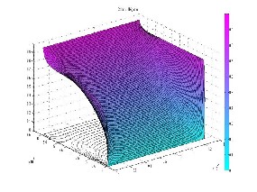
Exact solution of Poisson’s equation is analytically computed employing Finite Element Method (FEM) with the help of 'pde' toolbox from Matlab (Figure 1). The Surface potential is calculated from this solution. Thus the depletion width td computed using the surface potential so obtained gives more exact result as compared to the assumed values of surface potential.![]()
EOT=t HK
HK
).. .. . .. . (5 )
Dielectric constants and bandgaps of highk materials needed for computation are given in TableI. [10]
GATE MATERIAL
DIELECTRIC CONSTANT K
ENERGY BAND GAP (Eg)
Figure–1: Potential Contour in Channel of NMOSFET,Distance along Xaxis represents channel width, Distance along Yaxis represents
SiO2 3.9 9
TiO2 80 3.5
HfO2 25 6
Ta2O5 25 4.4
Al2 O3 8 8.8
ZrO2 25 5.8
ZrSixOy 812 6.5
channel length, Distance along Zaxis represents channel potential
The analytical expression of DIBL is expected to provide better agreement with simulated results and as it is expected to yield more accurate value of the dielectric thickness td .
Y2O3 | 13 | 6 | |
Ya2O3 | 27 | 4.3 | III. Results and discussions: |
Choice of gate oxide depends on permittivity K and energy band gap Eg. Table 1 indicates a few good quality dielectric materials. Here HfO2 is the material of choice because of its highK value and high band gap energy.
In this computation of DIBL parameter, the depletion width td in expression 2 is derived by solving twodimensional (2D) Poisson's equation.
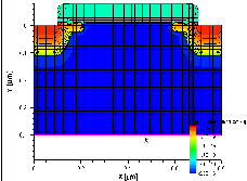
The simulation is done on the 45nm
MOSFET shown in figure 2:
δ2 Ψ
δ2 y
− ρ
δx 2 + δy 2 =
. .. .. . .. .. . .. ( 6)
ε
with total space charge density given by
ρ(x,y)={p(x,y)+Nd+ n(x,y) Na}............(7)
where n(x,y) and p(x,y) are electron and hole densities, Na and Nd+ are the ionised acceptors and donors respectively.
From equation 5 and 6 we have,![]() .......(8)
.......(8)
Figure – 2 : 45nm MOSFET after meshing, colour bar indicates the corresponding electron doping concentration
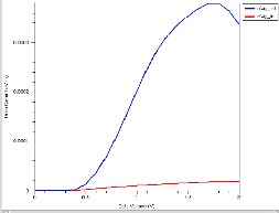
The effect of DIBl on drain current is shown in figure 3 where the drain field has ten folds increased the current current.
Subhradip Das is currently pursuing research assistant(TEyIBengal Univerest P Phase II funded) at West Bengal University of Technology, India, Phone07278210724, Email: subhradipdas85e@gmail.com
Sudakshina Kundu, professor & Head, Department of Computer Science & Engineering, West Bengal University of
Technology, India, Email: sudakshin.kundu@wbut.ac.in
IJSER © 2013 http://www.ijser.org
International Journal of Scientific & Engineering Research, Volume 4, Issue 8, August-2013
ISSN 2229-5518
1255
Figure –3: IdVg Curve (saturation and linear):Gate
Voltage along Xaxis and Drain current along Yaxis
The effect of variation of design parameters on DIBL as obtained from simulated results are shown. TCAD SENTAURUS is used to simulate the nMOSFET. Data is plotted in Matlab Software.
The results in figures 4 – 8 demonstrate the varitaion of DIBL parameter with the design partameters; substrate doping (Fig. 4), oxide thickness (Fig. 5), temperature (fig. 6), junction depth (Fig. 7) and drainsource voltage (Fig. 8).
Analytical results calculated from the expression given in reference [6] based on onedimensional Poisson's equation, do not agree with well the simulated results. It is found that the deviation of calculated values diverge from the simulated ones. As the field in the channel increases the need for including the fringe effects and solving the twodimensional potentials increase. By merely incorporating surface potential computed from solving the 2D Poissons equation into the expression 2 [6] will not agree with the simulation unless the expression 2 is modified using the small channel effects. Hence we have opted for empirical modelling in order to obtain an accurate empirical model that will efficiently describe the DIBL effect to design engineers.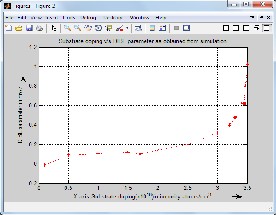
Figure – 4: DIBL vs Substrate doping:
DIBL along Yaxis, Substrate doping along Xaxis
Figure – 5: DIBL vs Ox ide Thickness (in nm): DIBL along Yaxis, tOX (in nm) along Xaxis
Figure–6: DIBL vs Temperature (in Kelvin): DIBL along Yaxis, T (in Kelvin) along Xaxis

Figure – 7: DIBL vs Juntion dept(in nm):
DIBL along Yaxis, Juntion dept along Xaxis
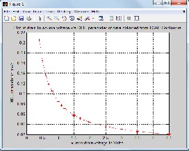
Figure 8 : DIBL vs drainsource voltage (in mV): DIBL along Yaxis, VDS along Xaxis
Subhradip Das is currently pursuing research assistant(TEyIBengal Univerest P Phase II funded) at West Bengal University of Technology, India, Phone07278210724, Email: subhradipdas85e@gmail.com
Sudakshina Kundu, professor & Head, Department of Computer Science & Engineering, West Bengal University of
Technology, India, Email: sudakshin.kundu@wbut.ac.in
IJSER © 2013 http://www.ijser.org
International Journal of Scientific & Engineering Research, Volume 4, Issue 8, August-2013
ISSN 2229-5518
1256
There is a clear mismatch between the theoretical values of DIBL parameters and their simulated results. An empirical model is proposed for to correctly account for the effects of the design parameters. Empirical relations for the DIBL parameter for each individual design parameter, keeping others constant, are obtained by Polynomial Curve Fitting using Matlab® tool. It is assumed that individual effects of the design parameters are linearly separable.
Drain to Source Voltage: Curve fitting of DIBL with Vds can be with a 6th order polynomial. The curve is shown below (Fig 9). The empirical formula explaining the variation is
P1 = [ 0.0017x0 - 0.0269x1 + 0.1731x2 - 0.5689x3 +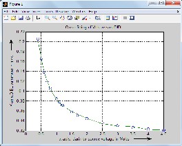
1.0179x4 - 0.9763x5 + 0.4625x6 ]
Figure -9: Curve fitting of DIBL with Vds:
DIBL along Yaxis, VDS (in mV) along Xaxis
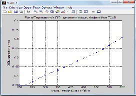
of temperature with DIBL is a 1st order one. The relationship is P3 = [0.0007x0-0.0927x1]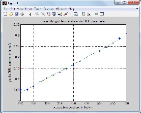
Figure11: Curve fitting of DIBL with Temperature,
DIBL along Yaxis, T(in Kelvin) along Xaxis
Oxide thickness: The polynomial for curve fitting the variation of oxide thickness with DIBL is a 2nd order one. The curve fitting parameters are given in the row matrix P4 = [0.136x0 + .128x1]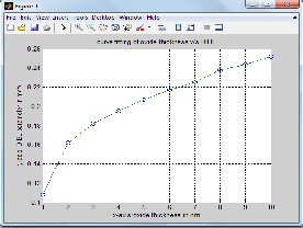
depth (Fig 10) gives a 13th order polynomial with the following fitting curve
DIBL along Yaxis, tOX
(in nm) along Xaxis
P2=[0.0x0 + 0.0x1 + 0.0x2 + 0.0x3 + 0.0x4 - 0.0012x5 +
0.0223x6 - 0.3127x7 + 3.2005x8 - 23.5756x9 +
121.4860x10 - 414.5655x11 + 839.2957x12 –
760.8183x13]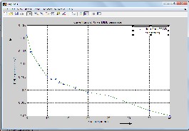
Figure10: Curve fitting of DIBL with junction depth:
DIBL along Yaxis, tOX in nm) along Xaxis
substrate doping is a 13th order polynomial:
P5 = [0.0001x0 – 0.0016x1+ 0.0126x2 0.0658x3 +
0.239x4 0.6201x5+ 1.1554x6 1.5329x7 + 1.4120x8
0.8607x9 + 0.3179x10 0.0595x11 + 0.0035x12] .108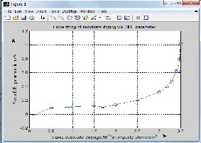
: DIBL along Yaxis, Substrate doping along Xaxis
Subhradip Das is currently pursuing research assistant(TEyIBengal Univerest P Phase II funded) at West Bengal University of Technology, India, Phone07278210724, Email: subhradipdas85e@gmail.com
Sudakshina Kundu, professor & Head, Department of Computer Science & Engineering, West Bengal University of
Technology, India, Email: sudakshin.kundu@wbut.ac.in
IJSER © 2013 http://www.ijser.org
International Journal of Scientific & Engineering Research, Volume 4, Issue 8, August-2013
ISSN 2229-5518
1257
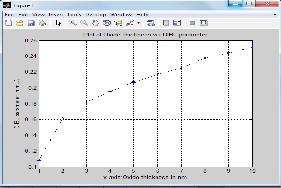
In 45nm conventional nMOSFET with oxide barrier, the effect of DIBL becomes significant. The effect of DIBL can be reduced if the silicon dioxide is replaced by a highK material with greater thickness. This thickness is refereed to as Effective Oxide Thickness (EOT). Fig. 14 plots the EOT (computed by equation 5) against permittivity for different highK dielectrics. With the increase of permittivity for highK dielectric, equivalent oxide thickness decreases. A wider highK material can be used for channel isolation with the same effect as that of a much narrower oxide and hence the gate control over the channel remains unchanged but tunnel current is reduced. The effect of DIBL will decrease if a highK material with lower EOT is used. Thus the choice of highK dielectric improves the device behaviour at nano dimensions.
Plot of Equivalent Oxide Thickness vs. permittivity
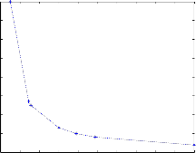
80
70
60
50
40
30
20
10
0
0 0.1 0.2 0.3 0.4 0.5 0.6 0.7 0.8 0.9 1
It is therefore concluded that as the device is scaled down, DIBL becomes more and more pronounced. Hence gate geometry related solutions are sought for. But if the insulator thickness can be scaled down, the DIBL will be reduced which is definitely a positive effect of scaling.
Subhradip Das would sincerely thank Prof. Sudakshina Kundu for her through supervision and inspiration. This is incomplete unless heartist thanks goes to Dr. Sanatan Chatterjee. This work is funded by TEQIP Phase II Project and laboratory facilties are provided by WBUT. Special thanks to Sumalya Ghosh and Rajesh Dutta of the Department of Computer Science & Engineering, WBUT, KOLKATA, INDIA, for their useful discussions.
[1] G.E.Moore, “Progress in digital integrated electronics,”
in Proc. IEDM Tech. Dig., 1975, pp. 1113
[2] Wolfgang Arden, Michel Brillouët, Patrick Cogez, Mart Graef, Bert Huizing, Reinhard Mahnkop, “MorethanMooreWhitePaper”, http://www.itrs.net/Links/2010ITRS/IRCITRSMtMv2
[3] Taur and Tak H. Ning, Fundamentals of Modern VLSI Devices. New York: Cambridge Univ. Press 1998, ch.3, pp.
176179.
[4] Ayhan A. Mutlu, and Mahmud Rahman,
Equivalent Oxide Thickness(nm)
x 1 -9
“TwoDimensional Analytical Model for Drain Induced
Barrier Lowering (DIBL) in Short Channel MOSFETs”, Proc. IEEE Southeastcon, 2000, Pp. 340344
Fig. 14: Variation of EOT with permittivity
Effect of change of dielectric material is accounted for by the varying EOT. Effect of different insulating materials with different dielectric constants can be easily incorporated by computing the Effective Oxide Thicknesses. Alternatively, the EOT will help in calculating the thicknesses of the highK materials needed for a particular DIBL parameter.
If a highK dielectric layer is grown on substrate itself the interface becomes unstable due to mismatch in the lattice constant of the insulator and substrate. This causes increase in scattering and hence mobility degradation. Hence a solution is [7] to grow a lowK dielectric layer above the substrate and then grow the highK layer. This will increase the EOT thus affecting the DIBL parameter.
[5] Savvas G. Chamberlain Sannasi Ramanan,” DrainInduced BarrierLowering analysis in VLSI MOSFET devices using twodimensional numerical simulation” IEEE TRANSACTIONS ON ELECTRON DEVICES, VOLED33, NO. 11, NOVEMBERR 1986
[6] S.S. Mahato. P. Chakraborty, T.K. Maiti, M.K.Bera, C. Mahata, M. Sengupta, A. Chakraborty, S.K.Sarkar & C.K.Maiti,” DIBL in shortchannel strainedSi nMOSFET”, IEEE CONFERENCE PUBLICATION, 2008, pages 1 4.
[7] M.H. Chowdhury, M.A.Mannan and S.A.Mahmood,” High–K dielectric for submicron MOSFET”, IJETSE International Journal of Emerging Technologies in Science and Engineering, Vol.2, No.2, July 2010
[8] Narain Arora, ‘Threshold voltage’ MOSFET Modeling for VLSI Simulation Theory and Practice, International Series on Advances in Solid State Electronics and Technology, ASSET, 2007,ch8, Sec5.3.3, pp210218.
[9] Marlia Morsin et al, “Design, Simulation and Characterization of 50nm pwell MOSFET Using Sentaurus TCAD Software”, Malaysian Technical Universities Conference on Engineering and Technology, June 2022, 2009.
[10] S.M.Sze, Physics of semiconductor device, ‘Mosfet’, A Wileyinterscience publication, John Wiley and Sons, Ed. 2, Ch.8, pp. 469485.
Subhradip Das is currently pursuing research assistant(TEyIBengal Univerest P Phase II funded) at West Bengal University of Technology, India, Phone07278210724, Email: subhradipdas85e@gmail.com
Sudakshina Kundu, professor & Head, Department of Computer Science & Engineering, West Bengal University of
Technology, India, Email: sudakshin.kundu@wbut.ac.in
IJSER © 2013 http://www.ijser.org