International Journal of Scientific & Engineering Research Volume 2, Issue 9, September-2011 1
ISSN 2229-5518
Embedding Soft processor based
USB device driver on FPGA
Prof. Shashank Pujari
Abstract— Embedding a System on a Programmable Chip with in the constraint of available resources brings out ingenuity of a SoPC designer. The paper covers an efficient Soft processor based USB communication device driver implementation on FPGA using a 10% foot print so as to set aside the rest 90% of the logic resources of the programmable chip for other compute and control intensive tasks. Using a Soft processor on FPGA to interface a peripheral is a convenient choice so that the task of the device driver development can be off loaded to a software developer. Software developer takes a black box approach and uses the programmer model of the Soft processor and this is where things can go wrong. SoPC designer looks critically at the device driver requirement and brings in hardware/software co-design approach to think out of the box to meet the challenges of the constraint aware embedded design in terms of cost, size, memory, performance and time to market.
Index Terms— Device Driver, Embedded, FPGA, Soft Processor, SOPC,
—————————— ——————————
SB is an integral part of an embedded system requiring communication between host PC and target system. There are two types of USB controllers available in the market, one hav- ing built in Microcontroller and other without it. The micro- controller based USB controller has built in device driver, which handles all data communication tasks, is an easy choice but not very cost effective for small-embedded design targeted for $10 cost. For example Cypress CY7C68013A- 16A family USB controller has 8051 core and the unit cost is $5 which is not economical for use in a $10 cost FPGA based embedded product. To design a low cost FPGA based embedded system, the cost of the USB2.0 device and the selection of FPGA should be proper. In this paper a NXP USB 2.0 controller ISP1582 cost- ing $3 and $10 Spartan-3 FPGA device from Xilinx are used.
For FPGA based design requiring USB data communication, it is desirable to build the USB driver along with target design in the FPGA. The USB interface logic should use minimal re- sources of FPGA to accommodate other main logics. Present paper discusses issues and solutions for embedding USB driv- er in FPGA in a cost effective manner by a memory efficient design. The hardware-software co-design approach is based on the embedded soft processor and internal memory in side FPGA. An 8-bit RISC Soft Micro Controller (SMC) core namely PicoBlaze offered by Xilinx is used. The small footprint PicoB- laze supports 1K Byte of instruction memory, which is not sufficient to hold the complete USB device driver. A technique for increasing the size of the instruction memory
————————————————
Prof. Shashank Pujari is currently with Sambalpur University Institute of Information Technology (www.suiit.ac.in) , Jyotivihar, Burla, Sambalpur, Orissa-768019
pujarishashank@gmail.com
by using a switchable tri-pair memory bank, there by scaling the addressability of the soft processor, is the key motivation behind this paper.
The paper is organized as follows; Soft processor is intro- duced in section II, section III covers USB device driver flow, section IV covers Design Implementation; section V covers Hardware/software co-design approach with Tri-pair switch- ed memory bank. Concluding remark is given in section VI followed by acknowledgement and reference.
The PicoBlaze SMC core is embedded within the target FPGA and requires no external resources. The SMC is opti- mized for efficiency and low deployment cost. It occupies just
96 FPGA slices, or only 20% of an XC3S200 FPGA. The SMC performs a respectable 44 to 100 million instructions per second (MIPS) depending on the target FPGA family and speed grade. The SMC works at 50 MIPS, high enough to han- dle High-speed data rate (480Mbits) of USB2.0 controller. Pi- coBlaze SMC is delivered as synthesizable VHDL source code and hence the core is future-proof and flexible enough to be adapted to future FPGA architectures, effectively eliminating fears of product obsolescence. Being integrated within the FPGA, the PicoBlaze SMC reduces board space, design cost, and inventory.
A suite of development tools supports the PicoBlaze SMC software development, including an assembler, a graphical Integrated Development Environment (IDE), a graphical in- struction set simulator.
For porting the Picoblaze SMC to FPGA devices of other vendors such as Altera and Actel, the VHDL code has been made vendor independent by using commonly available logic primitives of the FPGA [1].
IJSER © 2011
International Journal of Scientific & Engineering Research Volume 2, Issue 9, September-2011 2
ISSN 2229-5518
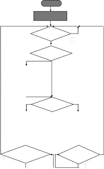
The USB device driver software flow chart is shown in Fig – 1. After power on reset, the registers of the USB controller ISP
1582 are initialized for high speed (480Mbits) data communi- cation, nos. of endpoint and DMA. Then the enumeration process begins, which establishes communication between the slave target USB device and the PC host. A set of descriptor is sent from the target USB device to the host that describes the device‘s USB capabilities and how they will be used. Next the application communication begins. The host sends read or write command to slave and in return the slave sends data packets requested by host or receives data packets from host respectively. All packet transactions are handled through in- terrupts under DMA control. All types of communication i.e., Bulk, Interrupt, Isochronous and Control are handled through proper initialization of USB device registers. The Processor program is stored in three ROMs as shown in flow chart in three respective shades i.e., Dark shade – ROM1 – All initiali- zations, Light shade – ROM2 – Enumeration, transmit and receive packet, No shade - ROM3 – USB decision control flow and descriptors.
The design was implemented on a Spartan3 XC3S200 device using Xilinx Kit, connected to a NXP ISP1582 device, over the general-purpose connectors A1 and A2 available on the kit. The clock speed of the FPGA device decides the speed of the USB communication. The System clock of USB interface is 80
MHz and sufficient for High-speed 480 Mbits/sec USB 2.0 performance. The VHDL code is compiled on Xilinx ISE 7.2
Software tools. The assembly language program of Soft Pro-
Y
RECEIVE
RESET
INIT USB REGISTERS & DMA
INTERRUPT PRESENT
N Y
USB ENUM INTERRUPT
N
ENDPOINT RECV /XMIT
TRANSMIT
cessor is compiled using KCPSM3 assembler. The internal and external components of SPARTAN XC3S200 are shown in Fig -
2 i.e., Soft Microcontroller, Read/write FIFO Interface, USB interface and an external NXP ISP1582 USB controller. Fig-3 shows the detailed internal blocks of the FPGA.
ENDPOINT
Y TRANSMIT-
N
ENDPOINT
RECEIVER
Y
N
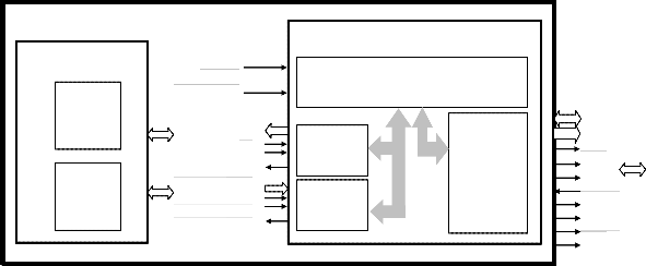
Fig- 1 Flow chart of USB device driver
SPARTAN XC3S200-4FT256 FPGA
OTHER LOGIC
RESET
SOFT
USB INTERFACE LOGIC
WRITE FIFO
READ FIFO
CLK_80MH
WRITE_ PORT FIFO FULL FIFO EMPTY WR_CLK READ PORT FIFO FULL FIFO EMPTY RD_CLK
MICROCONTROLLER
WRITE FIFO LOGIC
READ FIFO LOGIC
USB INTER- FACE LOGIC
USB_ADDR USB_DATA
CS WR RD DREQ
DACK DIOR DIOW
EOT
USB DEVICE
ISP 1582
Fig –2 FPGA System Block diagram
IJSER © 2011
International Journal of Scientific & Engineering Research Volume 2, Issue 9, September-2011 3
ISSN 2229-5518
The SMC is implemented using Xilinx Picoblaze core availa- ble with Xilinx Core Generator library. It has one 8 bit input port, one 8 bit output port and one 8 bit port ID for selection of 256 input or output ports. It has 10 bit ROM address and accepts 18 bit instruction code from ROM. This ROM is internal to the FPGA implemented using Block RAM. The processor fetches instruction in one clock period and executes in next clock period. There is one interrupt input and one interrupt acknowledge out- put. Multiple interrupts can be gated by an OR gate.
The SMC over all controls the sub blocks. It initializes the USB device and completes the Enumeration process and then waits for command from PC host. It generates Read FIFO con- trol signal, when it receives a USB read command from PC host. The Read FIFO control signal are used to read data stored in FIFO and then send it to USB. Similarly SMC gene- rates Write FIFO control signal when it receives a USB write command from PC host. The Write FIFO control signal are used to write data received from USB into FIFO.
PICOBLAZE PROCESSOR
USB_DATA
80MHz
RESET
PORT 0
ADD DATA PORT 5
PORT 1
PORT 2
PORT 0
INTR PORT 1
PORT 2
PORT 4
USB INTERFACE
USB_CS/ WE/
RE/
ADD [7:0]
USB_ADDR
CS_N RD_N
WR_N DREQ
DACK DIOW DIOR EOT
INT
FIFO_DATA
10 MHz
TIMER
START STOP
FIFO_EMPTY FULL_INTR CS/
WE/
RE/
A0
A1
A2
FIFO INTERFACE![]()
RD_FIFO_FULL RD_FIFO_EMPTY
RD_FIFO_EN RD_FIFO_CLK
![]()
WR_FIFO_FULL WR_FIFO_EMPTY
WR_FIFO_EN WR_FIFO_CLK
Fig – 3 FPGA functional block diagram
IJSER © 2011
International Journal of Scientific & Engineering Research Volume 2, Issue 9, September-2011 4
ISSN 2229-5518
The ROM is implemented inside the FPGA using Block RAM. The ROM code is created by a standard text editor and assembled using the KPCSM3 assembler provided by Xilinx. The instruction set is provided in the user guide of the Pico- blaze Processor. The ROM and the Soft Processor run by the same 80 MHz clock. The addressability of Pico Blaze Processor
NXP ISP1582 has 16bit wide data bus and 256 addressable registers and supports USB 2.0 standard. The USB controller uses a 16-bit data bus access. For single-byte registers, the up- per byte (MSB Byte) is ignored.
has been extended from 1K ROM to 3K ROM by address and instruction data multiplexor logic.
The FIFO collects data from other logic of the FPGA. The SMC monitors the FIFO empty and full signal during initial start up. The FIFO works on dual clock and operates on separate write and read clock. The depth and width of the FIFO are 512 Byte and 16 bit respectively for the present design but can be resized depending on applications. The SMC generates the FIFO enable and read/write clock to read/write data.
The USB interface connects to an external USB device NXP ISP1582. Additional DMA controller logic is implemented in the FPGA to transfer data in DMA mode as shown in Fig – 4 and explained in next paragraph. Interrupt generated by the USB de- vice controls the SMC program execution flow shown in flow chart Fig –1.
DATA [15:0]
ADDR [7:0]
RST CLK
RD WR
ACK CS_USB
CS_DMA
USB_INT
USB COMMUNICA- TION INTERFACE
DMA CONTROL- LER
BLOCK RAM
DATA [15:0]
ADDR [7:0]
CS_N RD_N
WR_N DREQ
DACK DIOW
DIOR
EOT INT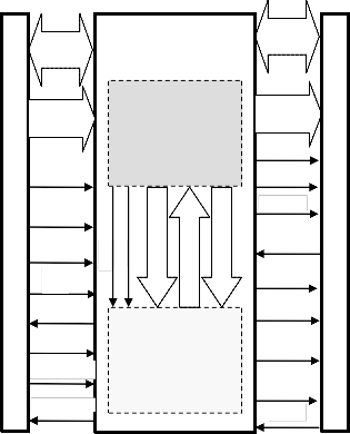
The USB data transfer rate is at high-speed (480 Mbit/s). The USB Interface has a DMA controller for fast data transfer from board to USB host and vice versa as explained in follow- ing section.
The USB controller NXP ISP1582 operates in slave mode and the DMA controller of FPGA in master mode. The DMA data will be stored in local Block RAM inside USB interface first and then transferred. For reading data from USB host the data is read by DMA and stored in local Block Ram and then forwarded to processor. For writing data to USB host, Proces- sor writes data to local Block Ram and then forwarded to USB host through DMA. This method is used for small chunk of data transfer. For large data transfer the DMA is directly be- tween the FIFO and the USB device NXP ISP1582. The DMA transaction per word is @80 nsec equivalent to 25 Mbytes/sec.
Fig – 4 USB interface with DMA controller interface
The design resource used in Spartan-3 device is shown in Ta- ble-1. The resource utilization shows that there is 70% of the total resources free to accommodate other logics of the system.
Table - 1 FPGA resource utilization
IJSER © 2011
International Journal of Scientific & Engineering Research Volume 2, Issue 9, September-2011 5
ISSN 2229-5518

The simplified flow chart of the USB device driver is shown in Fig-5. The driver has been partitioned in three main modules each occupying 1K. The USB registers are in- itialized in ROM1. The main program for enumeration process, transmit and receive data packet is managed in second ROM2. Third ROM3 occupies decision control flow and assorted subroutine functions including descriptor de- tails. The memory bank switch program flowchart is shown in Fig-6. This program is there at the end of each ROM as shown in Table 2-3-4, which links the software modules res- ident in three separate ROMs. The associated VHDL code is given and its equivalent hardware is shown in Fig- 7.
MEMORY_SWITCH_FROM_ROM1_ TO_ ROM2:
ADDRESS | 3EE | |
0X3EE 0X3EF 0X3F0 | LOAD OUTPUT NOP | Port Data, 01 Port Data, FF |


Table 3 – MEMORY SWITCH PROGRAM IN ROM2
MEMORY_SWITCH_FROM_ROM2_ TO_ ROM3:
ADDRESS 3E8
0X3E8 LOAD Port Data, 02
0X3E9 OUTPUT Port Data, PORT_SEL NOP
MEMORY_SWITCH_FROM_ROM3_ TO_ ROM2:
ADDRESS 3EE
0X3EC NOP
0X3ED JUMP ROM3_TO_ROM2_PROG
MEMORY_SWITCH_FROM_ROM1_ TO_ ROM2:
Device In- itialization ROM1
Main Program ROM2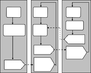
Fig-5 Device driver flow
Subroutine Functions ROM3
ADDRESS 3F0
0X3F0 NOP
0X3F1 JUMP ROM2_START

Table 4 – MEMORY SWITCH PROGRAM IN ROM3
ROM1
Rom1
Start
ROM2
Rom2
Start
ROM3
Rom3
Start
MEMORY_SWITCH_FROM_ROM2_ TO_ ROM3:
Device In- itialization
Jump to
Rom2
Main
Pro-
Jump to
Rom3
Jump to
Rom2
Start
Subrou- tine Func-
Jump to
Rom2
Jump to
Rom3
Start
; VHDL CODE FOR ADDRESS & DATA MUX
addr1 <= address when sel_rom = "00" else x"3FF";
addr2 <= address when sel_rom = "01" else x"3FF";
addr3 <= address when sel_rom = "10" else x"3FF";
instruction <= instr1 when sel_rom = "00" else
instr2 when sel_rom = "01" else
instr3 when sel_rom = "10";
sel_rom <= When (Port_sel = 1) then Port_data(1 downto 0)
else sel_rom;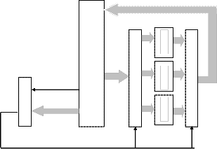
Instruction
Fig-6 Memory Banks switch flow chart
The simulation diagram can be understood with ref- erence to Table –2. It is seen that while switching from ROM1 to ROM2, the continuity of processor execution is maintained. A dummy instruction ‗NOP‘ is inserted at the same address of both ROM1 and ROM2. Actually there is no ‗NOP‘ instruction in Picoblaze, it is mentioned for simplicity of explanation. Ac- tual instruction used is ―AND s0, s0‖, which means logical
―ANDING‖ of the register s0 with it self. The total overhead of
switching between ROMs is 4 instructions.
PORTSEL PORT DATA
SEL ROM [1:0]
Fig- 7 Hardware equivalent of above VHDL code for Memory
Bank switch
Table 2 –MEMORY SWITCH PROGRAM IN ROM1
IJSER © 2011
International Journal of Scientific & Engineering Research Volume 2, Issue 9, September-2011 6
ISSN 2229-5518
USB communication protocol stack was ported to an em- bedded target system on a FPGA with minimal usage of logic resources. A unique methodology of extending the address ability of the PicoBlaze Soft Microcontroller from 1K to 3K, by address and data multiplexing, was devised to accommodate the USB driver.
Scope of the paper can be extended in future for comparative study of a modified Picoblaze designed for 3K ROM addressabil- ity with the present design as well as with a Dynamically Partial- ly Reconfigurable FPGA, where instead of switching between the three ROMs, ROMs are replaced by downloading the next ROM on a clock boundary.
[1] Farhad Marchant, Shashank Pujari, Manish Patil ―Plat- form Independent 8-bit Soft core for SoPC‖, International Multiconference of Engineers and Computer Scientists
2009, Hong Kong, 18 March, 2009
[2] Technical specs of Xilinx FPGA Spartan 3, NXP USB
ISP1582;
[3] Xilinx ISE 7.2, Chipscope & Modelsim tools manuals.
[4] USB 2.0 standard specification.
[5] Jan Axelson ―USB Complete‖
[6] www.nxp.com
[7] www.xilinx.com
IJSER © 2011