Inte rnatio nal Jo urnal o f Sc ie ntific & Eng inee ring Re se arc h Vo lume 3, Issue 3, Marc h -2012 1
ISS N 2229-5518
Design of Low power, Low Jitter Ring Oscillator
Using 50nm CMOS Technology
Nidhi Thakur
—————————— —————————
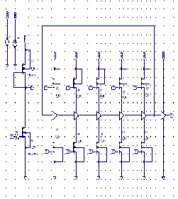
.Among many other oscillator topologies the ring oscillator is attractive for its high fr equency ,w ide r ange of operation
and small die size. A r ing oscillator consists of multiple
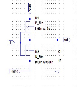
VCO is a fr equency modulated oscillator whose instantaneous output fr equency is dir ectly pr oportional to its contr ol voltage .A r ing oscillator can be smoothly integr ated in a standar d CMOS pr ocess w ithout taking extra pr ocessing steps because it does not r equir e any passive r esonant element compar e to CMOS LC-tank oscillator [6], [7], [8].In this w or k 5-stage CMOS inverter forms a closed path with positive feedback [10]. The schematic of the whole VCO is shown in fig 1.Voltage contr ol oscillator have a CMOS inverter circuit as shown in figur e2.This inverter cir cuit is connected to curr ent sour ces M3 and M4 that limit the curr ent available to the inverter . The curr ents in MOSFETs M1 and M2 ar e mirr or ed in each invert er stage.
The oscillation fr equency is given by –
stages of delay cells. Delay cell can be design w ith differ ential pair and CMOS inverter . In this paper CMOS
f = I d
inverter is used as a delay cell [7].
———— ——— ——— ——— ———
o sc
Wher e,
N .
to t DD
N= Number of stages
I d = I d 3 = I d 4 = center drain curr ent
IJS ER © 2012 http :// www.ijser.org
International Journal of Scientific & Engineering Res earch Volume 3, Iss ue 3, Ma rch -2012 2
ISSN 2229-5518
Cto t = Cout + Cin (2)
Cto t = Cox ( W p . Lp + W n . Ln ) (3)
= Minimum fr equency
min
3 ,
![]()
Cin = 2 Cox ( W p . Lp + W n . Ln ) (4)
,
to t = 2 (
W p Lp + W
n . Ln
Figur e 2 Schematic view of CMOS inv erter
Figur e 1 Schematic view of VCO
Gain of the VCO is the slope of the curves given in fig3.It is defined as
max
min
VCO designed such that its oscillation fr equency is contr olled by input voltage. For communication it is impor tant to have a lar ge tuning range among the other structur e of VCO r ing oscillator has a lar ge tuning r ange![]()
KVCO = 2∏
max
min
r adian/ v.s (7)
[4].Tuning range is shown in fig 3. Tuning r ange can be
defined as-
It is the inter val between two times of maximum effect (or
minimum effect) of a signal pr operty that varies r egular ly with time. It is defined as-
f f
Tuning range% = max min 100 (6)
f
Wher e
f = f
cen ter
= fr equency of oscillation![]()
![]()
t jitter 1 1
center
f
o sc
center
center
f
VCO
max = Maximum fr equency
IJS ER © 2012 http :// www.ijser.org
International Journal of Scientific & Engineering Res earch Volume 3, Iss ue 3, Ma rch -2012 3
ISSN 2229-5518
f
VCO = Var iation in the VCO’s output fr equency.
f
65nm and 180nm designs. The jitter for the cir cuit is 39.8pS. The per formance r esult of the Voltage contr ol oscillator compar ed with ear lier w or k is summar ized in Table 1.
center = fr equency of oscillation
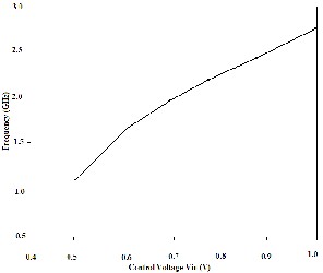
Figur e3: gr aphical r epr esentation of fr equency vs. voltage
The average pow er dissipated by the VCO is given as
[11]-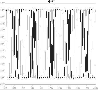
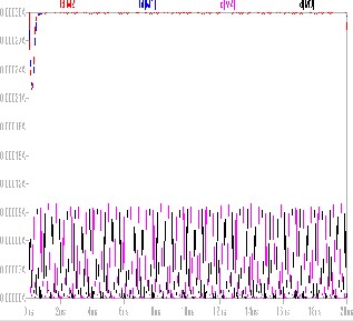
Figur e 4 Simulation r esult of output voltage vs. time
I a vg
= N.V
DD C
.
to t
o s c
avg
V DD . I avg
I a vg = I d (11)
avg
V DD . I d
The r ing oscillator for this w or k has been r ealized in 50nm
CMOS technology . The output fr equency can vary fr om
0.7GHz to 2.56GHz, the tuning range is found to be 72%
which is much better than what is r epor ted ear lier . At 2.56
GHz the aver age power consumption is 0.064mW at 1V
supply voltage which is also much lesser compar ed to
Figur e 5 Simulation r esult of drain curr ent
IJS ER © 2012 http :// www.ijser.org
International Journal of Scientific & Engineering Res earch Volume 3, Iss ue 3, Ma rch -2012 4
ISSN 2229-5518
[4] Lizhong Sun and Tadeusz A. Kwasniewski, “A
1.25-GHz 0.35-um Monolithic CMOS PLL Based on a Multiphase Ring Oscillator ”, IEEE Journal of Solid- State Circuits, pp.910-916, VOL. 36, JUNE 2001.
[5] M.Vamshi Krishna, J.Xie, M.A.Do, C.C.Boon, K.S.Yeo and Aar on, A 1.8-V 3.6-mW 2.4-GHz Fully integr ated CMOS Fr equency Synthesizer for IEEE
802.15.4, 18th IEEE/IFIP International Conference on
VLSI and System-on-Chip ,978-1-4244-6471, pp.387-
391, May 2010.
[6] Mehdi Ayat ,Behnam Babaei , Reza Ebrahimi Atani
, Sattar Mirzakuchaki and Babak Zamanlooy, “Design of A 100MHz - 1.66GHz, 0.13µm CMOS Phase Locked Loop”, International Conference on Electronic Devices, Systems and Applications , 978-1-
4244-6632-0, pp.154-158,2010.
[7] S. J. Lee, B. Kim, and K. Lee, “A novel high-speed r ing oscillator for multiphase clock generation using negative skew ed delay scheme,” IEEE Journal of Solid-State Circuits, pp. 289–291, vol. 32,
Feb-1997.
The design pr esented in a 50nm CMOS technology and is designed using CMOS inverter w ith curr ent mirror .The Voltage contr ol oscillator consumes power ar ound
0.064mW for 1V supply and the tuning r ange is 72%.
[1] Mike Shuo-W ei Chen et al, “A Calibr ation-Fr ee
800MHz Fractional-N Digital PLL with Embedded
TDC”, ISSCC, Febr uary 2010.
[2] Mostafa Savedi Oskooei, AliAfzali-Kusha, S.M Atar odi. “A High-Speed and Low-Power Voltage Contr olled Oscillator in 0.18-um CMOS Pr ocess”, IEEE Journal of Solid-State Circuits , pp.933-936, 2007.
[3] Neda Nouri and Shahr iar Mirabb asi, “A900MHZ-
2GHZ LOW-SW ING LOW-POW ER 0.18µM CMOS
PLL’’, IEEE CCECE/CCGEI, Saskatoon, 0-7803-
8886-0, pp.1558-1561, May 2005.
[8] C. H. Par k and B. Kim, “A Low-Noise 900 MHz VCO in 0.6 µm CMOS,” IEEE Journal of Solid State Circuits, pp. 586 – 591, 1999.
[9] Ali Hajimir i, Sotir ios Limotyrakis, and Thomas H.
Lee, “Jitter and Phase Noise in Ring Oscillator s”, IEEE Journal of Solid-State Circuits, 0018–9200/99, pp.790-804,VOL. 34, JUNE 1999.
[10] B. Razavi, “Design of Integr ated Cir cuits for Optical Communications”, McGraw-Hill, New Yor k, 2003.
[11] Ashish Raman and R. K. Sar in , “0.18-µm Low Pow er CMOS Ring Oscillator for Radio Fr equency Applications”, International Journal of Computer Theory and Engineering, pp.770-774, Vol. 3, December 2011.
IJS ER © 2012 http :// www.ijser.org
lnte rnationalJournal of Scientific & Engineering Research Volume 3, Issue 3,1\i'a rch-2012 5
ISSN 2229-5518
IJSER ©2012
http:1/W t>NV.i jser -cra