International Journal of Scientific & Engineering Research, Volume 4, Issue 7, July-2013 2413
ISSN 2229-5518
P. Sathees Kumar1, Prof. R. Jagadeesan2
1PG Scholar, EEE Department, SNS College of Engineering, Coimbatore, India
2HOD, EEE Department, SNS College of Engineering, Coimbatore, India
E-mail id: 1sathees61@gmail.com, 2jaga.padhu18@gmail.com
Keywords- Clock-gated, High-performance, low-power sense-amplifier flip-flop, Self-controllable Voltage Level
(SVL)
Very Large Scale Integration (VLSI) is the process of creating integrated circuits by combining thousands of transistors into a single chip. With the contraption of transistors at Bell labs, in 1947, the field of electronics got a new direction which shifted from power-consuming vacuum tubes to solid-state devices. In the past decades, Moore’s law drives the VLSI technology to continuously increase the transistor densities, there are hundred millions of
transistors or even billions of transistors on a chip
today, which in that the power consumption of VLSI chip has constantly been increasing. Although the capacitances and the power supply scale down meanwhile, the power consumption of the VLSI chip is still increasing continuously.
The schematic diagram of the static output- controlled discharge flip-flop (SCDFF) is illustrated in Figure 2.1 SCDFF involves an explicit pulse generator and a latch that captures the pulse signal. The latch structure of SCDFF consists of two static stages. In the first stage, input D is used to drive the precharge transistor so that node X follows D during the sampling period. In addition, the conditional discharging technique is implemented by inserting a QB-controlled NMOS in the discharge path, which prevents unnecessary discharging at node X as long as the input remains high. The major advantage of SCDFF is low power consumption and soft-edge property. However, a delay is always present between Q and QB due to the single-ended nature of SCDFF [1].
IJSER © 2013 http://www.ijser.org
International Journal of Scientific & Engineering Research, Volume 4, Issue 7, July-2013 2414
ISSN 2229-5518
Fig 2.1 STATIC OUTPUT-CONTROLLED DISCHARGE FLIP
FLOP: STATIC LATCH.
The dual-edge triggered static pulsed flip-flop (DSPFF) is shown in Figure.2.2 In its pulse generator, the four inverters are used to generate the inverted and delayed clock signals. These signals along with two NMOS pass transistors create a narrow sampling window at both the rising and falling edges of the clock [1].
Once the PULSE signal is generated, both pass transistors, N1 and N2, are turned on to capture the input data so that either SB or RB will be discharged. A smaller delay can be obtained from the DB and D are directly fed to the nodes, SB and RB, respectively. The PMOS transistors, P1 and P2, together with two weak NMOS transistors, N3 and N4, effectively avoid the floating of nodes SB and RB when the flip-flop is opaque, thereby providing a fully static operation. The explicit pulse generator is simple and suitable for dual-edge triggering. The static feature of DSPFF eliminates unnecessary transitions. Symmetrical output delay scans be obtained by carefully sizing the transistors aspect ratios. However, the flip-flop latency may be degraded due to the large capacitive loads at the SB and RB nodes. On top of that, DSPFF suffers from high leakage current. This is caused by a high-voltage drop across either transistor N3 or N4, when they are off [1].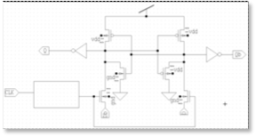
Fig 2.2. DUAL EDGE-TRIGGERED STATIC PULSED FLIP FLOP : STATIC LATCH.
The flip-flop used in the third generation of Digital Equipment Corporation’s 600-MHz Alpha processor was based on a static memory cell design. This particular flip-flop is known as a sense-amplifier flip- flop, (SAFF). The SAFF is also a time window-based flip-flop. The SAFF is a differential-input differential- output positive edge triggered flip-flop [8].
Timing elements, latches and flip-flops, are critical
to performance of digital systems, due to tighter timing constraints and low power requirements. Short setup and hold times are essential, but often overlooked.
Recently reported flip-flop structures achieved a
small delay between the latest point of data arrival and output transition. Typical representatives of these structures are sense amplifier-based flip-flop (SAFF), hybrid latch-flip-flop (HLFF) and semi-dynamic flip- flop (SDFF). Hybrid flip-flops outperform reported sense amplifier-based designs, because the latter is limited by the output latch implementation.
SAFF consists of the sense amplifier in the first stage and the R-S latch in the second stage. The first stage of this flip-flop is the sense amplifier. It senses the true and complementary differential inputs. The sense amplifier stage produces monotonous transitions from high to low logic level on one of the outputs following the leading clock edge. The S-R latch captures each transition and holds the state until
the next leading clock edge arrives. Therefore, the
IJSER © 2013 http://www.ijser.org
International Journal of Scientific & Engineering Research, Volume 4, Issue 7, July-2013 2415
ISSN 2229-5518
whole structure acts as a flip-flop. The SAFF is in
0.18nm effective channel length CMOS technology. Transistor sizing is optimized for both high speed and compact standard-cell layout [8].
The schematic diagram of adaptive clocking dual- edge triggered sense amplifier flip-flop (ACSAFF) is presented in Figure 2.3 and 2.4 ACSAFF is an implicit dual-edge triggered sense amplifier flip-flop. It consists of three stages, i.e., the adaptive clock inverting stage, the front-end sensing stage and the Nikolic’s latch stage. The adaptive clock inverter chain is designed to disable some internal clocked transistors when the data switching activity is low. The signal derived from node NC of the sensing stage is used to implement adaptive clocking. If input D is different from output Q, node NC will be pulled up, to turn on transistors N1 and N2. Consequently, the desired inverted and delayed signals, CLK3 and CLK4, will be produced so that an arrow transparent window is created on the rising or falling edges of the clock. Either SB or RB will be discharged during this transparent period, changing the output state in the latching stage. The design of adaptive clocking inverter chain is shown below [1].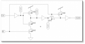
Fig 2.3 ADAPTIVE CLOCKING DUAL EDGE-TRIGGERED SENSE-AMPLIFIER FLIP FLOP: ADAPTIVE CLOCKING INVERTER CHAIN
Once the output state is altered, the charging path of NC is blocked and NC will be discharged through either N3 and N4 orN5 and N6, thereby disabling the inverter chain. When D is the same as Q, node NC is low and the flip-flop is opaque. Therefore, the adaptive clocking inverter chain will generate the pulse or will not generate the pulse according to the
input and output of the flip-flop. During the
transparent period of the adaptive clocking dual-edge
sense-amplifier flip-flop, either SB or RB will be discharged due to the input data. Then the output of the flip-flop will be changed on the latching stage.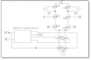
Fig 2.4 ADAPTIVE CLOCKING DUAL EDGE-TRIGGERED SENSE AMPLIFIER FLIP-FLOP FRONT END SENSING STAGE
Now, we begin to analyze the disadvantages
of the adaptive clocking dual-edge sense-amplifier flip-flop. As seen in the figure 2.5 The adaptive clocking dual-edge sense-amplifier flip-flop requires more transistors realize the adaptive clocking, and the circuit is very complex, so the speed of the flip- flop will be slower. Moreover, if the switching activity of the circuit is very high, the adaptive clocking dual- edge sense-amplifier flip-flop will consume a lot of power due to the more used transistors in the circuit.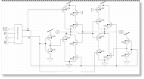
Fig 2.5 ADAPTIVE CLOCKING DUAL EDGE- TRIGGERED SENSE-AMPLIFIER FLIP FLOP: NIKOLIC’S LATCH.
In this section, two new dual edge-triggered sense- amplifier flip-flops are constructed and discussed. The first proposed flip-flop is named as dual edge- triggered sense-amplifier flip-flop (DET-SAFF) and
IJSER © 2013 http://www.ijser.org
International Journal of Scientific & Engineering Research, Volume 4, Issue 7, July-2013 2416
ISSN 2229-5518
the second one is clock gating sense-amplifier flip-
flop (CG-SAFF).
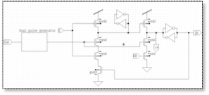
The schematic diagram of the proposed DET-SAFF is given in Figure 3.1 and 3.2 It consists of three stages: the pulse generating stage, the sensing stage and the latching stage. The simple pulse generator used in DET-SAFF [1]. The dual edge- triggered pulse generator produces a brief pulse signal synchronized at the rising and falling clock edges. The pulse generator can be shared by multiple flip-flop circuits when a group of flip-flops are located closely. For a sense amplifier based flip-flop, in the evaluation phase, as soon as D is low, SB will be set too high, and if D is high, RB will be set to high. Therefore, the conditional recharging technique is applied at the sensing stage of DET-SAFF, to avoid redundant transitions at major internal nodes. Two input con- trolled PMOS transistors, SP1 and SP2, are embedded in the precharge paths of nodes SB and RB, respectively. In this case, if D remains high for n cycles, SB may only be discharged in the first cycle. For the following (n-1) cycles, SB will be floating when PULS is low or fed to the low state DB when PULS is high. As for RB, it only needs to be precharged in the first cycle and remains at its high state for the remaining cycles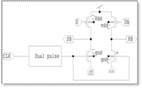
Fig 3.1 DUAL EDGE-TRIGGERED SENSE-AMPLIFIER FLIP FLOP: SENSING STAGE
Since the precharging activity is conditionally
controlled, the critical pull down the path of SB and RB is simplified, consisting of only one signal transistor. This helps to reduce the discharging time. It has some disadvantages and we will analyze it in the following paragraph.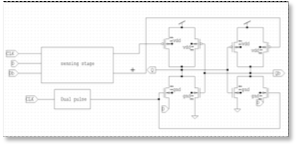
Fig 3.2 DUAL EDGE-TRIGGERED SENSE-AMPLIFIER FLIP FLOP: SYMMETRIC LATCH.
Similar to the Nikolic’s latch and Strollo’s latch , the new latch makes use of SB and RB to pull up the output nodes. But the pull down path is modified. It composes a PULS-controlled NMOS pass transistor, through which D (DB) is directly fed to the Q (QB) node. This topology significantly speeds up the high- to-low output transition because the output latch immediately captures the input value once the PULS signal is generated. On the other hand, the low-to- high latency will also be improved. This is because the output node will not only be charged by the pull- up transistors, LP1 and LP2, but also the pass transistors, LN1 and LN2. Note that the pass transistors cannot fully charge a node for high, but it can assist with the pull-up transition. The four inner transistors, LP3, LP4, LN3, and LN4, are used to hold the data in the flip-flop and maintain the output state when there is no pulse. For the proposed DETSAFF and previously mentioned dual edge designs, such as the SCDFF and DSPFF, the power saving techniques are only applicable for the latch part of the flip-flops. As the switching activity of the clock signal is 1, the pulse generator will always be operating even when the input invokes no output changes. These unnecessary transitions cause a lot of power to be
wasted, especially at low input switching activities.
IJSER © 2013 http://www.ijser.org
International Journal of Scientific & Engineering Research, Volume 4, Issue 7, July-2013 2417
ISSN 2229-5518
Now we begin to analyze the disadvantage of the
dual-edge triggered sense-amplifier flip-flop. In the pulse generator, the two inverters are used to generate delay for the clock, when the clock is from 0 to 1 (rising edge), because of the delay of the inverters, CLK2 cannot change from 0 to 1 immediately when CLK gets to 1, so there is a short time that when CLK is 1, CLK2 is 0. At this time, CP4 is on and the voltage of CLK will be transferred to pulse, so pulse can get to Vdd, then the pulse will drop down because CN3 is on at this time and CLK1 is low, but when the pulse is rising, CN3 has been already on and the voltage of the pulse will drop, because CLK1 can finish to change from 1 to 0 when a pulse is rising, the pulse cannot get to vdd and magnitude of the pulse will be lower than void. If we use this pulse generator to drive more flip-flops, it is possible that the magnitude of the pulse cannot get to the value which can open the NMOS in the sensing stage and latch.
On the sensing stage of the flip-flop, when there is
no pulse fed by the pulse generator and input data D is high, point SB will be floating, if the frequency of the clock is very low and D remains high for n cycles, the charges stored in point SB will leak out and SB will drop down from high voltage to low voltage, in this case, the logic of the flip-flop will be wrong. This structure of the sensing stage assumes that the frequency of the clock is very high and even if the point SB is floating, the voltage at point SB will keep high and will never drop down in this case.
3.2.1. Clock gating:
Clock gating is a popular technique used in many synchronous circuits for reducing dynamic power dissipation. Clock gating saves power by adding more logic to a circuit to prune the clock tree. Pruning the clock disables portions of the circuitry so that the flip flops in them do not have to switch states. Switching states consume power. When not
being switched, the switching power consumption
goes to zero, and only leakage currents are incurred. In order to eliminate the redundant transitions in
the pulse generator, the CG-SAFF is constructed. It
utilizes the DET-SAFF design as a baseline and incorporates the clock gating technique. In CG-SAFF, the clock gating technique is implemented by embedding a control circuit in the explicit pulse generator so that the PULS signal generation is disabled in a redundant event. The schematic and timing diagrams of the clock gated pulse generator are shown in Figure 3.3 below [1].
In order to compare the previous and current input
values, two comparators are applied to produce signals X and Y, by using the differential inputs, D and DB, and the buffered outputs, Q1 and QB1, as control signals. If D is different from the output Q1 (Q), X will be pulled up to high and Y to low. Transistor CN3 is turned on to allow the clock signal to pass through as CL. CL is known as the gated clock. At the same time, CP1 is on and drive the CLK1 signal to high before the rising edge of the clock. At the rising edge of the clock, CL is high and its delayed signal CLK3 remains low. Therefore, transistor CN5 and the transmission gate are turned on, driving the PULS signal to high. After a short period, the transparent window is closed as CLK1 goes low and CLK3 is pulled up. Thus, a short transparent period is created at the rising edge of the clock. Note that signal CLK1 is used for pulse generation rather than CLK2.At the falling edge of the clock, CL is low and CLK3 is high. Transistor CP5 is selected and generates a high PULS signal. The sampling window is shut down once CLK3 is low. When the input D remains the same in consecutive clock cycles, X is low and Y is high. CL is pulled down by CN4 so that the corresponding CLK3 will be low regardless of the CLK signal. CLK1 may only be discharged at the first clock cycle and maintains its low state in the remaining clock cycles. As a result, the flip-flop will remain opaque and thus, the power can be saved. The sensing and latching stages of the proposed CG-SAFF are illustrated in Figure 3.3 [1]. The sensing stage is the
same as DET-SAFF. Since the generated PULS signal
IJSER © 2013 http://www.ijser.org
International Journal of Scientific & Engineering Research, Volume 4, Issue 7, July-2013 2418
ISSN 2229-5518
is more heavily loaded than that of DET-SAFF, at
modified Nikolic’s latch is used.
Fig 3.3 CLOCK-GATED SENSE-AMPLIFIER FLIP FLOP: SENSING AND LATCHING STAGE.
It does not require any clock signal and provides the most stable operation. The inner holding topology is modified to obtain buffered differential outputs, Q1 and QB1, with reduced load capacitances. On the clocking stage, Q1 and QB1 are used to generate X and Y instead of using the Q and QB. This helps to improve the performance of CG-SAFF significantly.
The SVL circuit consists of an upper SVL (U- SVL) circuit and a lower SVL (L-SVL) circuit (Fig. 3.1), where a Clock Gated Sense Amplifier Flip Flop has been used as the load circuit. The U-SVL circuit is constructed of an extensive channel pull-up pMOSFET switch (PSW) and multiple nMOSFET resistor connected in series. Similarly, the L-SVL circuit incorporates a wide channel pull-down nMOSFET switch (nSW) and multiple series- connected pMOSFET resistors(pRSm)[12]. The Type III SVL circuit along with CG-SAFF is shown in Figure
4.1 The upper SVL consists of a single p-MOSFET
switch (p-SW) and m n-MOSFET switches (n-SW)
connected in series. The “on p-SW” connects a power
supply (VDD ) and load circuit in active mode, and “on n-SW” connect VDD and load circuit in standby mode.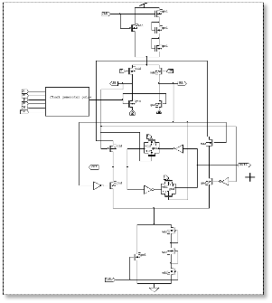
Fig 4.1 CIRCUIT DIAGRAM FOR CLOCK-GATED SENSE- AMPLIFIER FLIP FLOP WITH SVL CIRCUIT Similarly, the lower SVL circuit consists of
single n-MOSFET switch (n-SW) and m p-MOSFET switch connected in series, is located between a ground level (VSS ) and the load circuit. The lower SVL Circuit not only supplies VSS to the active load circuit through the “on n-SW” but also supplies VSS to the standby load circuit through the use of the “on p- SWs”. While the load circuit is active (i.e., CLB=“0” and CL=“1”), both the pSW and nSW are turned on, but the nRS1 and pRS1 are turned off. Therefore, the U-SVL and L-SVL circuits can supply a maximum supply voltage VD (=VDD) and a minimum ground- level voltage VS (=VSS=0), respectively, to the active load circuit. Thus, the operating speed of the load circuit can be maximized.
In the architecture of SAFF is analyzed on power consumption and delay during operation. It provides
IJSER © 2013 http://www.ijser.org
International Journal of Scientific & Engineering Research, Volume 4, Issue 7, July-2013 2419
ISSN 2229-5518
the detailed simulation analysis of SAFF. The schematic design and implemented by using Tanner tool. Tanner Tool provides fast, easy creation and editing of circuit schematics and also support a technology independent design methodology, allowing the user to choose a specific technology and vendor after completing the design. The circuit is characterized by using the 180nm technology which is having a supply voltage of 1.8volts. Circuit verification is done on the Tanner tool. Schematic of the simulation stages is designed for the S-Edit and net list simulation are done by using T-spice and waveforms are analyzed through the W-edit. The Simulation Stages include:
Existing Methods of
• Static Output-Controlled Discharge Flip-Flop
• Dual Edge-Triggered Static-Pulsed Flip-Flop
• Adaptive Clocking Dual Edge-Triggered
Sense-Amplifier Flip-Flop
• Dual-Edge Triggered Sense-Amplifier Flip- Flop and
• Clock-Gated Sense-Amplifier Flip-Flop
Proposed Method
• Clock-Gated Sense-Amplifier Flip-Flop with
SVL Circuit.
The following are the various input parameters used for the simulation stages
• DC Voltage: 1.8V
• Pulse Width: 10µm
• Length: 5µm
• Height: 5µm
• On value: 1.8V
• Off value: 0
• CMOS Technology used: 180nm technology
The Power Results for various Simulation stages is tabulated below.
TABLE1:OVER ALL POWER RESULTS COMPARISON
STAGES | AVERAGE POWER CONSUMPTION (Watts) | POWER DELAY PRODUCT (Watts microsecond) |
SCDFF | 4.7372 | 1.9876 x 10⁻³ |
DSPFF | 0.0963 | 1.9337 x10⁻³ |
ACSAFF | 3.1585 | -3 1.1959 x10 |
DET- SAFF | 4.4966 | 3.8063 x10⁻³ |
CG-SAFF | 0.0072 | 0.6686 x 10⁻³ |
Proposed CG-SAFF with SVL Circuit | 1.2982 | 0.6024x10⁻³ |
This paper presents two dual-edge triggered flip- flops for low power and high performance applications. The DET-SAFF achieves substantial power reduction by incorporating dual-edge triggering and conditional pre-charging. It also minimizes latency by utilizing a fast latch. But due to the continuous pulse generation operation in the DET-SAFF lot of power will be wasted. In order to eliminate the pulse generation the CGSAFF is introduced. It's embedded with control circuit to stop the pulse generation operation in unwanted times. So it achieves superior in power saving at low switching activities compared to DET-SAFF. As compared to ACSAFF, which also has a power saving pulse generator, CG-SAFF outperforms in terms of power consumption. Both versions of the proposed DET- SAFFs have conclusively proved their robustness and suitability of applications when low power and high
speed are of equal importance. The pulse generation
IJSER © 2013 http://www.ijser.org
International Journal of Scientific & Engineering Research, Volume 4, Issue 7, July-2013 2420
ISSN 2229-5518
circuits used in the proposed flip-flops show significant amount of power saving. By incorporating proposed SVL Circuit in the CG-SAFF increases the operating speed of the flip flop also decreases the maximum power consumption of the flip flop as compared to previous existing techniques. The low power consumption of the proposed CG-SAFF with SVL design suggests extensive using of these structures for future low-power applications.
This paper can be extended for the further work to reduce the average power consumption and delay by using other modified techniques.
[1] Myint Wai Phyu , Member , IEEE, Kangkang Fu, Wang Ling Goh, Senior Member, IEEE, and Kiat-Seng Yeo, Senior Member, IEEE, (Jan 2011) “Power –Efficient Explicit-Pulsed Dual Edge Triggered Sense-Amplifier Flip-Flops” in IEEE Trans. Very Large Scale Integr. (VLSI) Syst., vol. 19, no.1.pp 1-9
[2] Gong, Jianping, (2011) “Dual-edge triggered pulsed flip-flop with high performance and high soft-error tolerance” Electrical and Computer Engineering Master's Theses Paper 50.
[3] Peiyi Zhao et al. Peiyi Zhao, Member, IEEE, Jason McNeely, Student Member, IEEE, Pradeep Golconda, Magdy A. Bayoumi, Fellow, IEEE, Robert A. Barcenas, and Weidong Kuang (Mar.
2007) “Low-power clock branch sharing double edge-triggered
flip-flop,” IEEE Trans. Very Large Scale Integr. (VLSI) Syst. , vol.
15, no. 3, pp. 338–345.
[4] Yen-Ting Liu, Lih-YihChiou, and Soon-Jyh, (May 2006) “Energy-efficient adaptive clocking dual edge sense-amplifier flip-flop,” in Proc. IEEE Int. Symp. Circuits Systems (ISCAS
2006) , pp. 4329–4332.
[5] G. Aliakbar and M. Hamid, ( Jan. 2005)
“Dual-edge triggered static pulsed flip-flops,” in Proc. 18th Int.
Conf. VLSI Design 2005, pp. 846–849.
[6] P. Zhao, T. K. Darwish, and M. A. Bayoumi, (May 2004) “High-performance and low-power conditional discharge flip- flop,” IEEE Trans. Very Large Scale Integr. (VLSI) Syst. Vol. 12, no. 5, pp. 477–484.
[7] N. Nedovic, M. Aleksic, and V. G. Oklobdzija, (2002) “Conditional precharge techniques for power-efficient dual- edge clocking,” in Proc. 2002 Int. Symp. Low Power Electronics Design (ISPLED 2002) , pp. 56–59.
[8] BorivojeNikolic, VladimirStojanovic, VojinG. Oklobdzija, WenyanJia, JamesChiu, Michael Leung (1999), “Sense Amplifier- Based Flip-Flop” in 1999 IEEE International Solid State Circuits Conference.
[9] Massoud Pedram, (1995), “Design Technologies for Low Power VLSI” in Encyclopedia of Computer Science and Technology.
[10] Massoud Pedram, Qing Wu, Xunwei Wu, “A New Design for Double Edge Triggered Flip-Flop”, Asia and South Pacific Design Automation Conference (ASP-DAC), pp. 417-421.
[11] Tania Gupta and Rajesh Mehra Tania Gupta and Rajesh Mehra, “Efficient Explicit Pulsed Double Edge Triggered Flip- Flop by Using Dependency on Data” IOSR Journal of Electronics and Communication Engineering (IOSRJECE) ISSN
: 2278- 2834 Volume 2, Issue 1, PP 01-07.
[12] Tadayoshi Enomoto and Yuki Higuchi Chuo University, 1-13-27 Kasuga, Bunkyo-ku, Tokyo 112-8551,Japan.
IJSER © 2013 http://www.ijser.org
International Journal of Scientific & Engineering Research, Volume 4, Issue 7, July-2013 2421
ISSN 2229-5518
IJSER © 2013 http://www.ijser.org