International Journal of Scientific & Engineering Research, Volume 6, Issue 3, March-2015 811
ISSN 2229-5518
Design of High Efficiency Single Input Multiple
Output Converter
JASLIN DEENA. K SRUTHI.A
P.G. Scholar, Dept.of.EEE Assistant Professor, Dept. of EEE
jaslindeena21@gmail.com sruthia@skcet.ac.in
Sri Krishna College of Engineering & Technology Sri Krishna College of Engineering & Technology
Coimbatore Coimbatore
Abstract- The aim of this study is to develop a high-efficiency single-input multiple-output (SIMO) dc–dc converter. The converter proposed can boost the voltage of a low-voltage input power source to a controllable high-voltage dc and middle-voltage output terminals. The high-voltage dc can be taken as the main power for a high-voltage dc load or for the front terminal of a dc–ac inverter. Middle-voltage output terminals can supply powers for individual middle-voltage dc loads or for charging auxiliary power sources (e.g., battery modules). In this, a coupled-inductor with dc–dc converter scheme utilizes only one power switch with the properties of voltage clamping, soft switching, and the corresponding device specifications are designed. The switching pulse for the switch is provided by the PID and Fuzzy controller. As a result, the objectives of high-efficiency conversion, step- up ratio, and two output voltages with different levels can be obtained. The SIMO converter topology and its controllers are designed by using MATLAB/Simulink.
Index terms- SIMO, DC-DC converter, coupled-inductor, PID Controller, Fuzzy controller.
—————————— ——————————
1 INTRODUCTION
In today’s high-tech world the switching power supply market is flourishing quickly. Main target in power electronics is to convert electrical energy from one form to another. Power converters control the flow of power between two systems by changing the character of electrical energy from direct current to alternating current or vice versa, from one voltage level to another voltage or in some other way to make electrical energy to reach the load with highest efficiency is the target to be achieved. DC-DC converters are electronic circuits that change the DC operating voltage or current. They have recently aroused the interest in the current market due to its wide range of applicability. Reliability of the converters becomes a key to industrial focus. Electronic devices and control circuits must be highly robust in order to achieve a high standard life. A special concentration must be set on the total efficiency of the power electronic circuits, first because of the economic and environmental value of wasted power and, second because of the cost of energy dissipated that it can generate.
The simplest way to process power is using pulse
width modulation (PWM) control of the switch. These power
supplies are called switch mode power supplies (SMPS).
Keeping the switching frequency constant, the on time of the
switch is fixed to a predetermined pulse width, allowing the inductors/capacitors to store/supply the desired energy at the right time and place. Since the voltage across or current flowing through the switch is abruptly interrupted, this technique is also known as hard switching. Hard switching causes stress on the switches and introduce switching noise and power losses. The higher the switching frequency, the worse these problems become.
Another approach must be used to realize the desired high efficiency and higher power density converters. More
power density means higher switching frequencies using
smaller size and weight components. Switching frequencies in the neighborhood of 500 kHz to 10MHz [1] can provide the power required by such applications as the space satellites, space labs, laptop/notebook computers and electric vehicles.
2 LITERATURE REVIEW
Patra et al. [10] presented a SIMO dc–dc converter capable of generating buck, boost, and inverted outputs at the same time. Over three switches for one output were required for the circuit. The scheme is only suitable for the low output voltage and power application, and its power conversion efficiency is degenerated due to the operation of hard switching.
Nami et al. [11] proposed a new dc–dc multi-output boost
converter, which shares its total output between different
series of output voltages for low- and high-power applications. But, over two switches for one output were required for the converter, and its control scheme was complicated. Then, the corresponding output power cannot supply for individual loads independently.
Chen et al. [12] investigated a multiple-output dc–dc converter with shared zero-current- switching (ZCS) lagging leg. This converter with the soft-switching property can reduce the switching loss, the scheme with three full-bridge converters is much difficult, so the aim of high-efficiency power conversion is difficult, and its cost is inevitably increased.
Ko et al. [7] investigated a multi output converter
proposed switching combination, which does not require any special blocks, delivery of energy is always accomplished by flowing energy through an inductor, which leads to high energy conversion efficiency regardless of the balance between the buck and boost output loads. By adopting the newly proposed control sequence, input energy
IJSER © 2015 http://www.ijser.org
International Journal of Scientific & Engineering Research, Volume 6, Issue 3, March-2015 812
ISSN 2229-5518
can be delivered to the outputs through a lossless inductor continually without a current accumulation problem.
Wu et al. [24] studied a bidirectional isolated full-bridge dc- dc converter with active and passive snubbers. Although the converter in [24] has the properties of a conversion ratio nearly nine times, soft start-up, and features of soft-switching for battery charging/discharging, nine power switches and two transformer are required so that its manufacturing cost and volume will be greatly increased.
3 PROPOSED SIMO CONVERTER
The proposed SIMO converter uses one power switch to achieve the objectives of high-efficiency power, increase in step-up ratio, and different output levels of voltage. In the proposed SIMO converter, the soft switching techniques and clamping of voltage are adopted to reduce the switching and conduction losses via the utilization of a low-voltage-rated power switch with a small RDS (on). Because the slew rate of the current change in the coupled inductor can be restricted by the presence of leakage inductor, the current transition used to enable the power switch to turn ON with the property of ZCS, and the leakage inductor effect can alleviate the losses caused by the reverse-recovery current. Also, the problems of the stray inductance energy and reverse-recovery currents within diodes in the conventional boost converter also can be corrected, so that the high-efficiency conversion is achieved. The values of middle-voltage output terminals can be appropriately adjusted by the design of auxiliary inductors; the output voltage of the high-voltage dc bus can be stably controlled by a simple proportional-integral-derivative (Fuzzy) control.
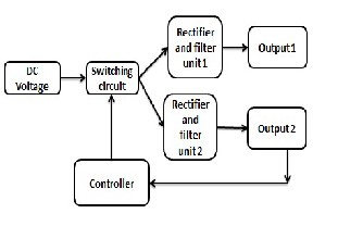
Fig.1 Block diagram of the proposed SIMO converter
3.1 Converter Design and Analysis
The system configuration of the proposed high- efficiency SIMO converter topology to generate two different voltage levels from a single-input power source is shown in Fig.2. The SIMO converter contains five parts including a low-voltage-side circuit (LVSC), a clamped circuit, the middle voltage circuit, the auxiliary circuit, and also the high voltage-side circuit (HVSC). The major symbol representations are summarized as follows. VFC (iFC) and VO1 (iO1) denote the voltages (currents) of the input power source and the output load at the LVSC and the auxiliary
circuit; V02 and i02 are the output voltage and current. CFC, CO1, and CO2 represent the filter capacitors in LVSC, auxiliary circuit, and the HVSC; C1 and C2 represents clamped and middle voltage capacitors in the clamped and middle-voltage circuits. LP and LS are the individual inductors in the primary and secondary sides of the coupled inductor Tr, where the primary side connected to the input power source; Laux is the auxiliary circuit inductor.
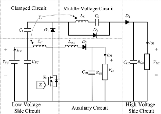
Fig.2 System configuration of high-efficiency single-input multiple-output (SIMO) converter.
The main switch is expressed as S1 in the LVSC; the equivalent load in the auxiliary circuit is characterized as RO1, and the output load is symbolized as RO2 in the HVSC. The corresponding equivalent circuit given in Fig.3 is used to define the voltage polarities and current directions. The coupled inductor in Fig.2 can be modeled as an ideal transformer including the magnetizing inductor Lmp and the leakage inductor Lkp in Fig.3.
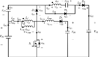
Fig.3. Equivalent circuit of SIMO Converter
The turns ratio N and coupling coefficient k of this ideal transformer are defined as
IJSER © 2015 http://www.ijser.org
International Journal of Scientific & Engineering Research, Volume 6, Issue 3, March-2015 813
ISSN 2229-5518
N = N 2 / N1

k = Lmp
(Lkp + Lmp)
= Lmp / Lp
(3.1) (3.2)
auxiliary circuit. Once the secondary side of the coupled inductor releases its leakage energy totally, and the diode D3 turns OFF, this mode ends.
Mode 4 (t3 –t4) [Fig. 4(d)]: At time t = t3, the main switch S1 is persistently turned OFF. As soon as the leakage energy has released from the primary side of the coupled inductor, the secondary current iLS is made in reverse
Where, N1 and N2 are the winding turns in the
primary and secondary sides of the coupled inductor are Tr. Because the voltage gain is less sensitive to the coupling coefficient and the clamped capacitor C1 is appropriately selected to completely absorb the leakage inductor energy [13], the coupling coefficient could be simply set at one (k =
1) to obtain Lmp = Lp via (3.2). In this study, the following assumptions are made to simplify the converter analyses: 1) The main switch including its body diode is assumed to be an ideal switching element; and 2) The conduction voltage drops of the switch and diodes are neglected.
3.2 Operation Modes
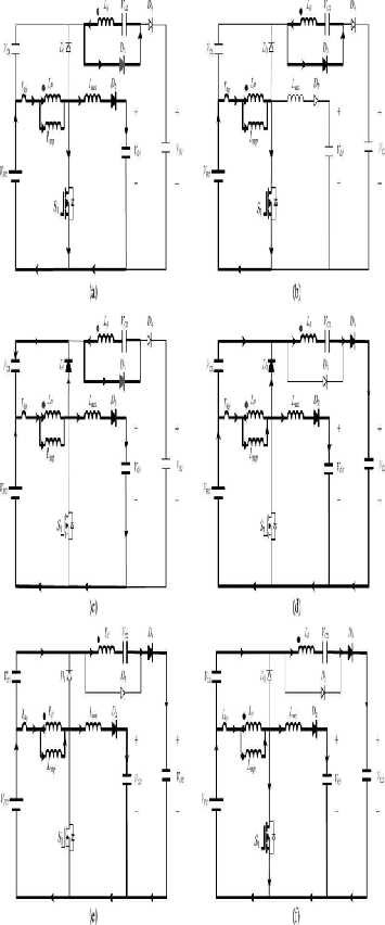
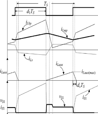
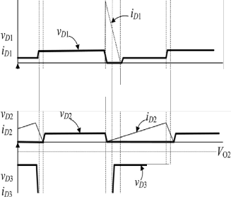
The characteristic waveforms are depicted in Fig.5, and the topological modes in one switching cycle are illustrated in Fig. 4.
Mode 1 (t0 –t1) [Fig. 4(a)]: In mode 1, the main switch S1
remained turned ON for a span and the diode D4 turned
OFF. Since the polarity of the windings of the coupled
inductor Tr is positive, the diode D3 goes ON. The
secondary current iLs reverses and charges to the middle- voltage capacitor C2. When the auxiliary inductor Lau x releases its stored energy entirely, and the diode D2 turns OFF, this mode ends.
Mode 2 (t1 –t2) [Fig. 4(b)]: At time t = t1, the main switch S1 is obstinately turned ON. As the primary
inductor LP is charged by the input power source, the magnetizing current iLmp increases progressively in an approximately linear way. Simultaneously, the secondary voltage vLs charges the middle-voltage capacitor C2 through the diode D3. Although the voltage vLmp is equal to the input volt- age VFC both at modes 1 and 2, the controlling slope of the leakage current of the coupled inductor (diLkp /dt) at modes 1 and 2 is different due to the path of the auxiliary circuit. For the auxiliary inductor Laux releases its stored energy totally, and the diode D2 turns OFF at the end of mode 1, it results in the reduction of diLkp / dt at mode 2.
Mode 3 (t2 –t3) [Fig. 4(c)]: At time t = t2, the main
switch S1 is turned OFF. Once the leakage energy still
released from the secondary side of the coupled inductor,
the diode D3 determinedly conducts and releases the leakage energy to the middle-voltage capacitor C2. While the voltage across the main switch vS1 is higher than the voltage across the clamped capacitor VC1, the diode D1 conducts to transfer the energy of the primary-side leakage inductor Lkp into the clamped capacitor C1. Together, partial energy of the primary-side leakage inductor Lkp is transmitted to the auxiliary inductor Laux, and the diode D2 conducts. Hence, the current iLaux passes through the diode D2 to supply the power for the output load in the
from the energy of the magnetizing inductor Lmp through
the ideal transformer, and runs through the diode D4 to
the HVSC. At one go, partial energy of the primary- side
leakage inductor Lkp is still persistently transmitted to the auxiliary inductor Lau x , and the diode D2 keeps to conduct. Moreover, the current iLaux passes through the diode D2 to supply the power for the output load in the auxiliary circuit.
Mode 5 (t4 –t5) [Fig. 4(e)]: At time t = t4, the main switch S1 is determinedly turned OFF, and the clamped diode D1 turns OFF because the primary leakage current iLkp equals to the auxiliary inductor current iLaux. In this mode, the input power source, the primary of the coupled inductor Tr, and the auxiliary inductor Lau x connect in series to supply the power for the output load in the auxiliary circuit through the diode D2 . At the same time, the input power source, the secondary of the coupled inductor Tr, the clamped capacitor C1, and the voltage capacitor (C2) connect in series to release the energy into the HVSC through the diode D4.
Mode6 (t5 –t6) [Fig. 4(f)]: At time t = t5, this mode begins
when the main switch S1 is activated. The auxiliary
inductor current iLaux needs time to decline to zero, the
diode D2 importunately conducts. In this mode, the input
source, the clamped capacitor C1, the secondary of the coupled inductor Tr, and the middle-voltage capacitor C2 is connected in series to release the energy into the HVSC through the diode D4.
Since the clamped diode D1 can be selected as a
low-voltage Schottky diode, it will be cut off quickly without a reverse-recovery current. Furthermore, the rising rate of the primary current iLkp is limited by the primary-side leakage inductor Lkp. So, one cannot derive any currents from the tracks of the HVSC, the middle- voltage circuit, the auxiliary circuit, and the clamped circuit. Accordingly, the main switch S1 is turned ON under the condition of ZCS and this soft-switching property is helpful for alleviating the switching loss. Once the secondary current iLS decays to zero, this mode finishes.
4 FUZZY CONTROLLER
A simple fuzzy logic control is built up by a group of rules based on the human knowledge of system behaviour. MATLAB/Simulink simulation model is built to study the dynamic behaviour of dc-to-dc converter and performance of offered controllers. Furthermore, design of fuzzy logic controller can provide desirable both small signal and large signal dynamic performance at same time, which is impossible with linear control technique.
IJSER © 2015 http://www.ijser.org
International Journal of Scientific & Engineering Research, Volume 6, Issue 3, March-2015 814
ISSN 2229-5518
The basic scheme of a fuzzy logic controller consists of four principal components such as: a Fuzzification interface, which converts input data into suitable linguistic values; a knowledge base, which consists of a data base with the necessary linguistic definitions and the control rule set; a Decision- Making logic which, simulating a human decision process, infer the fuzzy control action from the knowledge of the control rules and linguistic variable definitions; a Defuzzification interface which yields non fuzzy control action from an inferred fuzzy control action.
The boost dc-dc converter is a nonlinear function of the duty cycle because of the small signal model and its control method was applied to the control of boost converters. Fuzzy controllers do not involve an exact mathematical model. As an alternative, they are designed based on general knowledge of the plant. Fuzzy controllers are designed to adjust to varying operating points. Fuzzy Logic Controller is planned to control the output of boost dc-dc converter using Mamdani style fuzzy inference system. Two input variables, error (e) and change of error (de) are used in this fuzzy logic system. The single output variable (u) is duty cycle of PWM output. Fuzzy sets must be defined for each input and output variable. As shown in figure, five fuzzy subsets PB (Positive Big), PS (Positive Small), ZE (Zero), NS (Negative Small), NB (Negative Big) have been chosen for input variables error (e) and change of error (de).
Fig.4 Topological modes: (a) Mode 1 [t0 −t1 ]; (b) Mode 2 [t1 −t2 ]; (c) Mode 3 [t2 −t3 ]; (d) Mode 4 [t3 −t4 ]; (e) Mode 5 [t4 −t5 ]; (f)
Mode 6 [t5 −t6 ]
IJSER © 2015 http://www.ijser.org
International Journal of Scientific & Engineering Research, Volume 6, Issue 3, March-2015
ISSN 2229-5518
815
i:
; i
l Lmp r--..--
iLkp
l Ls
vm
i ;
J..._..-·········--·········--\ i ·-·-······-·· .
lD3

r--H··---------H ---- i i-------Vo2

i 
Fig.5 Characteristic waveform of high-efficiency SIMO converter.
IJSER IS) 2015
http://vvww ijser_org
International Journal of Scientific & Engineering Research, Volume 6, Issue 3, March-2015 816
ISSN 2229-5518
Fuzzy Logic Controller (FLC) is an attractive choice when precise mathematical formulations are unfeasible. Other advantages are:
• It can work with less precise inputs.
• It doesn’t need fast processors.
• It is extra robust than other non-linear controllers.
5 PID CONTROLLER
PID controller has all the necessary dynamics: fast reaction on change of the controller input (D mode), increase in control signal to lead error towards zero (I mode) and suitable action inside control error area to eliminate oscillations (P mode). Derivative mode improves stability of the system and enables increase in gain K and decrease in integral time constant Ti, which rises speed of the controller response [20].
PID controller is used when dealing with higher order capacitive processes (processes with more than one
energy storage) when their dynamic is not similar to the dynamics of an integrator (like in many thermal processes) [24]. PID controller is often used in industry, then also in the control of mobile objects (course and trajectory following included) when stability and precise reference following are essential. Conventional autopilot is for the most part PID type controllers.
Most of the industrial controllers are P-I-D in nature.
The major reasons behind the popularity of P-I-D
controller are its simplicity in structure and the
applicability to variety of processes [22]. Moreover the
controller can be tuned for a procedure, even without detailed mathematical model of the process. But, proper tuning of the controller parameters requires extensive experimentation.
As is evident from its name, the output of the PID controller u (t) can be expressed in terms of the input e(t), as:
Fig.6 Voltage waveform of medium step up converter using fuzzy controller
Fig.7 Voltage waveform of high step up converter using fuzzy controller
U (t ) = Kp[e(t ) + Td
de(t )

dt

+ 1 t e(t )dt
0
Fig.8 Voltage waveform of medium step up converter using PID controller
and the transfer function of the controller is given by:
C (s) = Kp[1 + Tds +

1 ]
Tis
The terms of the controller are defined as: Kp= Proportional gain Td= Derivative time and Ti= Integral time.
6 RESULTS AND DISCUSSION
The main aim of this converter design is to reduce the number of switches and achieving maximum efficiency by using a coupled inductor. The Zero Current Switching technique helps in the reduction in the voltage stress across the switch. The controller used is PID and Fuzzy Controller. The design of the converter along with the controller used is implemented using MATLAB/Simulink and the outputs are shown.
Fig.9 Voltage waveform of high step up converter using PID controller
7 CONCLUSION
A high-efficiency SIMO dc–dc converter has been developed, and this coupled-inductor-based converter
IJSER © 2015 http://www.ijser.org
International Journal of Scientific & Engineering Research, Volume 6, Issue 3, March-2015 817
ISSN 2229-5518
was applied well to a single-input power source with two output terminals composed of an auxiliary battery module and a high-voltage dc terminal. The proposed SIMO converter is suitable for the application requiring one common ground, which is preferable in most application. However, it is not advisable to be used as the active front for dc–ac multilevel inverters. This limitation is much to be investigated in the future research.
The advantages of the proposed SIMO converter are as follows: 1) this converter topology has only one switch to attain the purpose of high-efficiency conversion;
2) the voltage gain is increased by use of a coupled inductor; 3) the stray energy can be recycled by a clamped
capacitor into the auxiliary battery module to get the voltage clamping; 4) an auxiliary inductor is designed for assisting the switch turned ON under the condition of ZCS; 5) the switch voltage stress is not related to the input voltage.
REFERENCES
[1] A. Kirubakaran, S. Jain, and R. K. Nema, “DSP-controlled power electronic interface for fuel-cell-based distributed generation,” IEEE Trans. Power Electron., vol. 26, no. 12, pp. 3853–3864, Dec. 2011.
[2] B. Liu, S. Duan, and T. Cai, “Photovoltaic dc-building-module-
based BIPV system-concept and design considerations,” IEEE Trans. Power Electron., vol. 26, no. 5, pp. 1418–1429, May 2011.
[3] M. Singh and A. Chandra, “Application of adaptive network- based fuzzy interference system for sensorless control of PMSG- based wind turbine with nonlinear-load-compensation capabilities,” IEEE Trans. Power Electron., vol. 26, no. 1, pp. 165–175, Jan. 2011.
[4] C. T. Pan, M. C. Cheng, and C. M. Lai, “A novel integrated dc/ac converter with high voltage gain capability for distributed energy resource systems,” IEEE Trans. Power Electron., vol. 27, no. 5, pp.
2385–2395, May 2012.
[5] S. D. Gamini Jayasinghe, D. Mahinda Vilathgamuwa, and U. K. Madawala, “Diode-clamped three-level inverter-based battery/super capacitor direct integration scheme for renewable energy systems,” IEEE Trans. Power Electron., vol. 26, no. 6, pp. 3720–3729, Dec.2011. [6] H. Wu, R. Chen, J. Zhang, Y. Xing, H. Hu, and H. Ge, “A family of three- port half-bridge converters for a stand-alone renewable power system,” IEEE Trans. Power Electron., vol. 26, no. 9, pp. 2697–
2706, Sep. 2012.
[7] M. W. Ellis, M. R. Von Spakovsky, and D. J. Nelson, “Fuel cell systems: Efficient, flexible energy conversion for the 21st century,” Proc. IEEE, vol. 89, no. 12, pp. 1808–1818, Dec. 2001.
[8] T. Kim, O. Vodyakho, and J. Yang, “Fuel cell hybrid electronic scooter,” IEEE Ind. Appl. Mag., vol. 17, no. 2, pp. 25–31, Mar./Apr.
2011.
[9] F. Gao, B. Blunier, M. G. Simoes, and A. Miraoui, “PEM fuel cell stack modeling for real-time emulation in hardware-in-the-loop
application,” IEEE Trans. Energy Convers., vol. 26, no. 1, pp. 184–194, Mar. 2011.
[10] P. Patra, A. Patra, and N. Misra, “A single-inductor multiple- output switcher with simultaneous buck, boost and inverted outputs,” IEEE Trans. Power Electron., vol. 27, no. 4, pp. 1936–1951, Apr. 2012.
[11] A. Nami, F. Zare, A. Ghosh, and F. Blaabjerg, “Multiple-output
DC–DC converters based on diode-clamped converters configuration: Topology and control strategy,” IET Power Electron., vol. 3, no. 2, pp.
197–208, 2010.
[12] Y. Chen, Y. Kang, S. Nie, and X. Pei, “The multiple-output DC– DC converter with shared ZCS lagging leg,” IEEE Trans. Power Electron., vol. 26, no. 8, pp. 2278–2294, Aug. 2011.
[13] R. J. Wai and R. Y. Duan, “High step-up converter with coupled inductor,” IEEE Trans. Power Electron., vol. 20, no. 5, pp. 1025–1035, Sep. 2005.
[14] N. Mohan, T. M. Undeland, and W. P. Robbins, Power Electronics: Converters, Applications, and Design. New York: Wiley, 1995.
[15] L. Schuch, C. Rech, H. L. Hey, H. A. Grundling, H. Pinheiro, and
J. R. Pinheiro, “Analysis and design of a new high-efficiency bidirectional integrated ZVT PWM converter for DC-bus and battery- bank interface,” IEEE Trans. Ind. Appl., vol. 42, no. 5, pp. 1321–1332, Sep./Oct. 2006.
[16] Y. Chen and Y. Kang, “A full regulated dual-output dc-dc converter with special-connected two transformers (SCTTs) cell and complementary pulse width modulation-PFM(CPWM-PFM),” IEEE Trans. Power Electron., vol. 25, no. 5, pp. 1296–1309, May 2010.
[17] J. K. Kim, S. W. Choi, and G. W. Moon, “Zero-voltage switching
post regulation scheme for multi-output forward converter with synchronous switches,” IEEE Trans. Ind. Electron., vol. 58, no. 6, pp.
2378–2386, Jun. 2011.
[18] L. Hang, S. Wang, Y. Gu, W. Yao, and Z. Lu, “High cross- regulation multi-output LLC series resonant converter with Magamp post regulator,” IEEE Trans. Ind. Electron., vol. 58, no. 9, pp. 3905–
3913, Sep. 2011.
[19] S. H. Cho, C. S. Kim, and S. K. Han, “High-efficiency and low- cost tightly regulated dual-output LLC resonant converter,” IEEE Trans. Ind. Electron., vol. 59, no. 7, pp. 2982–2991, Jul. 2012.
[20] Gaurav, Amrit Kaur "Comparison between Conventional FUZZY and Fuzzy Logic Controller for Liquid Flow Control: Performance Evaluation of Fuzzy Logic and FUZZY Controller by Using MATLAB/Simulink" International Journal of Innovative Technology and Exploring Engineering (IJITEE). ISSN: 2278-3075, Volume-1, Issue-1, June 2012.
IJSER © 2015 http://www.ijser.org
International Journal of Scientific & Engineering Research, Volume 6, Issue 3, March-2015 818
ISSN 2229-5518
[21] Rajendra Meena "Simulation Study of Boost Converter with Various Control Techniques" International Journal of Science and Research (IJSR) ISSN (Online): 2319-7064.
[22] B. L. Narasimharaju, Satya Prakash Dubey, S. P. Singh, "Performance Evaluation of Fuzzy Logic Controlled Bidirectional DC to DC Converter" International Journal of Computing Science and Communication Technologies, VOL. 3, NO. 2, Jan. 2011.
[23] Sujata Verma, S.K Singh and A.G. Rao, "Overview of control Techniques for DC-DC converters" Research Journal of Engineering Sciences Vol. 2(8), 18-21, August (2013).
[24] Rajesh Kr Ahuja, Rajesh Kumar, "Design and Simulation of Fuzzy Logic Controller based Switched-Mode Power Supply" IPASJ International Journal of Electrical Engineering Volume 2, Issue 5, May 2014.
[25] Pulla Sravani Kumari, Kasthuri Gunavardhan, "DC-DC Converter with Coupled Inductor for Multiple-Outputs" International Journal of Advanced Research in Electrical, Electronics and Instrumentation Engineering Vol. 3, Issue 9, September 2014.
[26] S. K. Anuja, R. Satheesh Kumar, "A High Efficient DC-DC Converter with Soft Switching for Stress Reduction" International Conference on VLSI, Communication & Instrumentation (ICVCI)
2011.
[27] Thulasi V. S, H. Satish Kumar, "Single-Input Double Output High Efficient Boost DC–DC Converter" International of Modern Engineering Research (IJMER)" Vol. 4 Iss. 3 Mar. 2014.
IJSER © 2015 http://www.ijser.org