International Journal of Scientific & Engineering Research Volume 2, Issue 9, September-2011 1
ISSN 2229-5518
Design of Control unit for Low Power ALU Using Reversible Logic
Ravish Aradhya H V, Praveen Kumar B V, Muralidhara K N
Abstract—Technology advances in VLSI designs offer exponentially shrinking device dimensions and exponentially growing circuit complexities. However, device scaling is critically limited by the power dissipation; demanding for better power optimizations methods. Reversible Logic is becoming more and more prominent special optimization technique having its applications in Low Power CMOS designs, Quantum Computing and Nanotechnology. ALU is a fundamental building block of a central processing unit (CPU) in any computing system; reversible arithmetic unit has a high power optimization on the offer. By using suitable control logic to one of the input variables of parallel adder, various arithmetic operations can be realized. In this paper, as a part of ALU design, a Reversible low power control unit for arithmetic operations is proposed. In our design, the full Adders are realized using synthesizable, low quantum cost, low garbage output Peres gates. In this paper data transfer, addition, subtraction, increment, decrement and many other Arithmetic operations are realized using reversible gates.
Index Terms— Fredkin Gate, Garbage output, Low Power, Power Optimization, Quantum Cost, Reversible control Unit, Reversible Logic.
—————————— ——————————
esign of a control unit for any computing unit is the toughest part and involves more critical constraints. Power consumption is an important issue in modern day VLSI designs. The advancement in VLSI designs and particularly portable device technologies and increasingly high computation requirements, lead to the design of faster, smaller and more complex electronic Systems. The advent of multi-giga-hertz processors, high-end electronic gadgets bring with them an increase in system complexity, high density packages and a concern on power consumption. Power optimization can be done at various abstraction levels in CMOS VLSI design. At the Device (Technology) level, techniques such as VT reduction, multi-threshold voltages, gate oxide thickness, length and width variations are more common. At Circuit level, techniques such as use of alternate devices, network re- structuring, at Logic level, techniques such as use of alternate logic styles, energy recovery methods are common. At Architecture (System) level and Algorithmic level, techniques such as use of parallel structures, pipelining, state machine encoding, alternate encoding methods, etc are more common. Ref. [23] offers one such method at circuit and logic level, the energy recovery method, which employs reversible
logic concepts.
![]()
Ravish Aradhya H V is an associate professor and Praveen Kumar B V is a Masters student in Electronics and Communication Engineering Department, R V college of Engineering, Bangalore 560 059, India. E-mail: ravisharadhya@rvce.edu.in
Muralidhara K N is professor and Head in Electronics and Communication
Engineering Department, P E S college of Engineering, Mandya 571 401, India.
In 1973, C. H. Bennett [1,3] concluded that no energy would be dissipated from a system as long as the system was able to return to its initial state from its final state regardless of what occurred in between. It made clear that, for power not to be dissipated in the arbitrary circuit, it must be built from reversible gate. Reversible circuits are of particular interest in low power CMOS VLSI design.
2. REVERSIBLE GATES
The basic and simplest Reversible gate is conventional NOT gate and is a 1*1 gate. Controlled NOT (CNOT) gate is an example for a Reversible 2*2 gate. There are many 3*3
Reversible gates such as FG, TG, PG and Fredkin Gate.
The Quantum Cost of 1*1 Reversible gates is zero and Quantum Cost of 2*2 Reversible gates is one. Any Reversible gate is realized by using 1*1 NOT gates and 2*2
Reversible gates, such as V, V+ (V is square root of NOT
gate and V+ is its hermitian) and FG gate which is also known as CNOT gate. The V and V+ Quantum gates have the property given in the Equations 1, 2 and 3.
V * V = NOT ……………… (1) V * V+ = V+ * V = I ……….. (2) V+ * V+ = NOT ……………. (3)
The Quantum Cost of a Reversible gate is calculated by
counting the number of V, V+ and CNOT gates. There are several popular Reversible gates among the designers; Fredkin and Peres being emphasized here.![]()
Feynman / CNOT Gate: The Reversible 2*2 gate with Quantum Cost of one having mapping input (A, B) to output (P = A, Q = A B) is the basic reversible gate (However, the basic Reversible 1*1 gate without any control input is a CMOS NOT Gate and its Quantum Cost is zero).
IJSER © 2011 http://www.ijser.org
International Journal of Scientific & Engineering Research Volume 2, Issue 9, September-2011 2
ISSN 2229-5518
Toffoli gate: The Reversible 3*3 gate with three inputs and
![]()
three outputs where the inputs (A, B, C) are mapped to the outputs (P=A, Q=B, R=A.B C) has Quantum Cost of 5 and requires 2V, 1 V+ and 2 CNOT gates.
Peres Gate: The three inputs and three outputs i.e., 3*3 reversible gate having inputs (A, B, C) mapping to outputs (P = A, Q = AÅ B, R = (A.B) Å C).
Since it requires 2 V+, 1 V and 1 CNOT gate, it has the Quantum cost of 4. The Peres gate and its Quantum implementation are shown in the Fig. 1.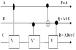
a. Logic Symbol b. Quantum implementation
Fig. 1 Reversible Peres Gate (PG)
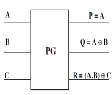
Fredkin Gate: Reversible 3*3 gate maps inputs (A, B, C) to outputs (P=A, Q=A'B+AC, R=AB+A'C) having Quantum cost of 5 and it requires two dotted rectangles, is equivalent to a 2*2 Feynman gate with Quantum cost of each dotted rectangle is 1, 1 V and 2 CNOT gates. Fredkin gate and its Quantum implementations are shown in Fig. 2.
a. Logic Symbol b. Quantum implementation
Fig. 2 Reversible Fredkin gate (FG)
3. LITERATURE SURVEY
R. Landauer’s *2] showed, the amount of energy (heat) dissipated for every irreversible bit operation is given by KT ln2, where K is the Boltzmann’s constant (1.3807×10⁻²³
JK-1) and T is the operating temperature. At room temperature (300 K), KT ln2 is approximately 2.8×10⁻²¹ J, which is small but not negligible. He also showed that only the logically irreversible steps in a computation carry an unavoidable energy penalty. If we could compute entirely with reversible operations, there would be no lower limit on energy consumption.
Bennett showed that kTln2 energy dissipation would not
occur, if a computation is carried out in a reversible way [1], since the amount of energy dissipated in a system bears a direct relationship to the number of bits erased during computation. He presented his idea in terms of a Turing machine, the abstract model of a computer that reads, writes and erases symbols on a tape. Erasures make the standard Turing machine irreversible, so Bennett added a second tape, called the history tape, where the machine keeps notes about erased or overwritten data. At the end of a computation, the final answer can be copied onto yet another tape for safekeeping. Then the machine is put in reverse gear, and with the help of the history tape, all the operations are undone, one by one, until the system returns to its initial condition. Yingtao Jiang, Abdulkarim Al-Sheraidah, Yuke Wang, Edwin Sha and Jin-Gyun Chung [12] have proposed low-power multiplexer-based
1-bit full adder that uses only 12 transistors and the new adder has more than 26% in power savings over conventional 28-transistor CMOS adder. Also, it consumes
23% less power than another 10-transistor adder and is
64% faster. Anantha P. Chandrakasan, Samuel Sheng, and Robert W. Brodersen [4] have given techniques for low- power operations, which can use the lowest possible supply voltage coupled with architectural, logic style, circuit and technology optimizations. Dmitri Maslov and Gerhard W. Dueck [13] introduced a synthesis model and a synthesis procedure which allow us to minimize the number of garbage outputs in reversible circuit and also showed that the new gates differ only marginally from the generalized Toffoli gates. Alberto Nannarelli and Tomás Lang [14] have illustrated some techniques for dividers realized in CMOS technology and energy dissipation reduction is carried out at different levels of abstraction: from the algorithm level down to the implementation or gate level. They also described the use of techniques such as switching-off non- active blocks, re-timing, dual voltage, and equalizing the paths to reduce glitches. Vivek V. Shende, Aditya K. Prasad, Igor L. Markov, and John P. Hayes [15] have synthesized oracle circuits for Grover’s search algorithm and shown a significant improvement over previously proposed synthesis algorithms and also showed constructively that every even permutation can be implemented without temporary storage using NOT, CNOT and TOFFOLI gates. William C. Athas, Lars “J”
,Svensson, Jeffrey G. koller, Nestoras Tzartzanis, and Eric Ying – Chin Chou[16] have showed that circuit energy can be conserved rather than dissipated as heat. Yvan Van Rentergem and Alexis De Vos [5] presented four designs for Reversible full-adder circuits and the implementation
IJSER © 2011 http://www.ijser.org
International Journal of Scientific & Engineering Research Volume 2, Issue 9, September-2011 3
ISSN 2229-5518
of these logic circuits into electronic circuitry based on
CMOS technology and pass-transistor design. Himanshu Thapliyal and Srinivas [11] proposed a 3x3 Reversible TKS gate with two of its outputs working as 2:1 multiplexer. The gate used to design a Reversible half adder and further used to design multiplexer based Reversible full adder. Rekha James et al., [17] proposed an implementation of Binary Coded Decimal adder in Reversible logic, which is basis of ALU for reversible CPU. Majid Mohammadi et al., [6] proposed a synthesis method to realize a Reversible Binary Coded Decimal adder/subtractor circuit. Genetic algorithms and don’t care concepts used to design and optimize all parts of a Binary Coded Decimal adder circuit in terms of number of garbage inputs/outputs and quantum cost. Lihui Ni et al., [18] described general approach to construct the Reversible full adder and can be extended to a variety of Reversible full adders with only two Reversible gates. Hasan, H.B., R. Islam, A.R. chowdhury and S.M.A chowdhury [20], proposed full adder circuit using Toffoli, Khan and Feynman gates with gates cost equal to 3, 2 garbage outputs and 1 constant input. Similarly, Perkowski M., L. Jozwiak, P. Kerntopf, A. Misohchenko and A. Al-Rabadi [21] proposed another full adder with only Toffoli and Feynman gates, with gates cost equal to 4, 2 garbage outputs and 1 constant input. Azad khan, M.H [24] proposed full adder with only Kahn and Feynman gates, with gates cost equal to 3, 3 garbage outputs and 2 constant input. Bruce, J.W., M.A. Thornton, L. shivakuamaraiah, P.S. kokate and X. Li [25], used only Fredkin gates to construct full adder with gates cost equal to 4, 3 garbage outputs and 2 constant input. Rangaraju H G [10] discussed various adder/subtractor circuit designs and showed that design III is good and optimized. Md. Saiful Islam, Muhammad Mahbubur Rahman, Zerina begum, and Mohd. Zulfiquar Hafiz [7], designed full adder circuit using IG gates and MIG gates with constant inputs of 2 and Garbage output of 3, and designed Fault Tolerant Reversible Carry Look-Ahead and Carry-Skip Adders. Bart Desoete, Alexis De Vos[8] used generalized Feynman’s three gates to arbitrary control gates and designed reversible 4-bit carry-look-ahead adder. In Ref. [22] design of complete processing unit is discussed using conventional logic. Same logic discussed in [22] is being used in our work. In Ref. [23] various low power VLSI techniques for power reduction and optimization are discussed. Saiful Islam and Rafiqul Islam [9], came up with good design for full adder using Peres gate with gates cost equal to 2, 2 garbage outputs and 1 constant input and this design is used in our implementation of arithmetic unit.
4. METHODOLOGY
Full-adder composition | No. of Gates used | No. of Garbag e output s | No. of consta nt inputs | Qu ant um cost s |
Peres gates Toffoli, Khan and Feynman gates Toffoli and Feynman gates Khan and Feynman gates Fredkin gates | 2 3 4 3 4 | 2 2 2 3 3 | 1 1 1 2 2 | 8 - 10 - 20 |
As proposed in [9] a full adder constructed using Peres gates is more efficient in terms of quantum cost as compared to a full adder constructed using Toffoli gates, Fredkin gate. The quantum cost of Toffoli gate is 5, Fredkin gate is also 5 and that of Peres gate is only 4[9]. Further, the Quantum costs of a Full adder constructed using PG, a combination of TG and FG, Fredkin gate is shown Table-1[9]. (Note: Quantum cost of Khan Gate is not known hence quantum cost of those adders involving this gate is not calculated)
Table-1 Cost comparison of different FAs
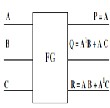
Hence, full adder constructed using Peres gate is used and a Full adder connected in cascade can be used to construct a parallel adder which forms the basic building block of arithmetic unit. As indicated in [22], by controlling one of the inputs to adder (B inputs for arithmetic operations and A inputs for logic operations), various arithmetic and logic operations can be realized; as illustrated in the Fig. 3.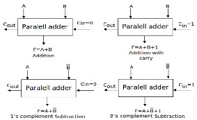
Fig. 3 Bi control for various operations from a parallel adder
IJSER © 2011 http://www.ijser.org
International Journal of Scientific & Engineering Research Volume 2, Issue 9, September-2011 4
ISSN 2229-5518
By controlling B input of the parallel adder following
operations can be performed:
When A & B inputs receive binary numbers and
Cin is zero, an addition operation is performed.
When A & B inputs receive binary numbers and Cin is 1, an addition with carry operation is performed.
If all bits of B input are complemented, then A
plus 1's complement of B operation is performed while keeping Cin zero.
When Cin is 1 and all bits of B input are complemented, then subtraction of An inputs and B inputs is performed (2's complement addition is same as subtraction).
Similarly, many other operations can also be realized. Ref. [22] suggests the control circuit for Bi input that provide the functionality called as true/complement, one/zero element. This block is shown Fig 4. It also suggests the control circuit for Ai input that provide the functionality for basic logic operations. This block is shown Fig 5.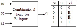
Fig. 4 Arithmetic Control element
In Fig. 4, S0, S1 and Cin are selection variables that are used to control the Bi inputs. Different arithmetic (including transfer) operations that can be performed from this circuit are summarized in the Table 2. Here Yi input is functionality of S0, S1 & Bi; depending on the values on S0 and S1, Bi input is manipulated and applied to Yi. Adding the value Yi in each case to value of a plus the Cin value gives the arithmetic operation in each entry.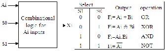
Fig. 5 Logic Control element
In Fig. 5, S0, S1 are selection variables that are used to
control the Ai inputs.
Different logical operations that can be performed from
this circuit are summarized in the Table 2.
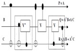
Here Xi input is functionality of S0, S1 & Ai. The full adder is constructed using two peres gates. The complete control unit with reversible logic gate can be realized as in Fig. 6.
The designed circuit has three control signals with a provision for realizing eight arithmetic operations and four logic operations. Three control variables S2, S1, S0 along with Cin select twelve different arithmetic-logic operations, and the S2 distinguishes between arithmetic and logic operations. The Ai and Bi inputs are altered depending on the S0, S1and S2 values and applied as input to full adder using Peres gates. Fig. 7 gives the simulation result of the designed ALU for two operations addition and subtraction. The CMOS implementation of control logic for 1-bit arithmetic and logic unit is shown in Fig. 8. The logic shown in Fig. 9 is 1-bit reversible arithmetic and logic unit with necessary control logic. This 1-bit ALU can be extended to any number bits required.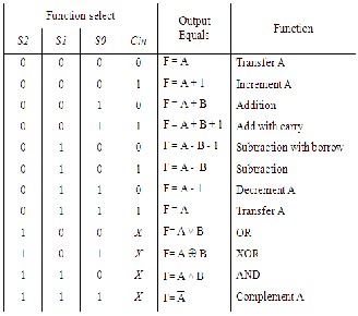
Table 2 Arithmetic operations
5. RESULTS
Reversible Full Adder/Subtractor and Reversible eight-bit Parallel Binary Adder/Subtractor are implemented using Python code and some of the sample results are simulated.
IJSER © 2011 http://www.ijser.org
International Journal of Scientific & Engineering Research Volume 2, Issue 9, September-2011 5
ISSN 2229-5518
The individual gate functionality is also simulated and implemented. In addition, simulation of some of the functions is carried out using Cadence Spectrae simulator and the overall logic is successfully simulated, simulation results are shown in shown in Fig. 7.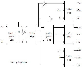
The above control unit is implemented using RevKit. The circuit of Fig. 6 is synthesized and simulated on RevKit and simulation results are recorded as in Fig. 9. The circuit of Fig. 8 was simulated for various input values and functionality of the circuit was verified. The circuit has 4 constant inputs and 8 garbage output. This will pave the way for design of a reversible logic processor unit. So that days are not far behind that we can get complete reversible processor.
Fig. 6 Reversible control logic for full adder
6. CONCLUSIONS
The Reversible gates are used to implement arithmetic circuit using Full Adder/Subtractor and Reversible control circuit for the Adder/Subtractor. The Reversible eight-bit Parallel Binary Adder/Subtractor is built using efficient design with minimum quantum cost, minimum garbage and minimum area and power overheads. The proposed design implementation of Reversible arithmetic unit using Parallel Binary Adder/Subtractor has better performance as compared to existing designs in terms of number of gates used, Garbage outputs and Quantum Cost and hence can be used for low power applications. In future, the design can be extended to any number of bits for Parallel Binary Adder/Subtractor unit and also for low power Reversible ALUs, Multipliers and Dividers.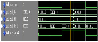
Fig. 7 Simulation results of Reversible Parallel Binary
Adder/Subtractor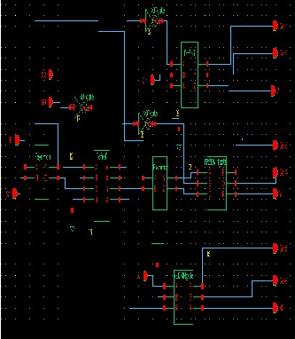
Fig. 8 Reversible 1 Bit ALU
IJSER © 2011 http://www.ijser.org
International Journal of Scientific & Engineering Research Volume 2, Issue 9, September-2011 6
ISSN 2229-5518
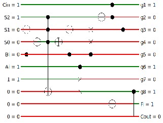
Fig. 9 Synthesized Reversible 1 Bit ALU
7. REFERENCES
[1]. C.H. Bennett , “Logical Reversibility of Computation”, IBM Journal of Research and Development, pp. 525-532, November 1973
[2]. R. Landauer, “Irreversibility and Heat Generation in the Computational Process”, IBM Journal of Research and Development, 5, pp. 183-191, 1961
[3]. C.H. Bennett, (1998) "Notes on the History of Reversible Computation", IBM Journal of Research and Development, vol. 32, pp. 16-23.
[4]. Anantha P. Chandrakasan, Samuel Sheng, and Robert W.
Brodersen,” Low-Power CMOS Digital Design”, IEEE journal of Solid –State circuits.Vol.27,No. 4, April 1992 .
[5]. Yvan Van Rentergem and Alexis De Vos, (2005) “Optimal Design of a Reversible Full Adder”, International Journal of Unconventional Computing, vol. 1, pp. 339 – 355.
[6]. Majid Mohammadi, Mohammad Eshghi, Majid Haghparast and Abbas Bahrololoom, (2008) “Design and Optimization of Reversible BCD Adder/Subtractor Circuit for Quantum and Nanotechnology Based Systems”, World Applied Sciences Journal, vol. 4, no. 6, pp. 787-792.
[7]. Md. Saiful Islam, Muhammad Mahbubur Rahman, Zerina begum, and Mohd. Zulfiquar Hafiz “ Efficient Approaches for Designing Fault Tolerant Reversible Carry Look-Ahead and Carry- Skip Adders”, MASAUM Journal of Basic and Applied Sciences, Vol. 1, No. 3, October 2009

[8]. Bart Desoete, Alexis De Vos “A reversible carry-look-ahead adder using control gates”, Science direct, INTEGRATION, the VLSI journal 33 (2002) 89–104.
[9]. Saiful Islam and Rafiqul Islam “Minimization of Reversible
Adder circuits”, Asian Journal of Information Technology
4(12) 1146-1151, 2005.
[10]. Rangaraju H G et al,”Low Power Reversible Parallel Binary Adder/Subtractor”, International journal of VLSI design & Communication Systems (VLSICS) Vol.1, No.3, September
2010.
[11]. Himanshu Thapliyal and M B Srinivas, “Novel Design and
Reversible Logic Synthesis of Multiplexer Based Full Adder and
Multipliers”, Forty Eight Midwest Symposium on Circuits and
Systems, vol. 2, pp. 1593 – 20061596.
[12]. Yingtao Jiang, Abdulkarim Al-Sheraidah, Yuke Wang, Edwin Sha, and Jin-Gyun Chung, ”A Novel Multiplexer-Based Low-Power Full Adder”, IEEE Transactions on circuits and systems -II: express briefs,vol. 51,No. 7 July 2004
[13]. Dmitri Maslov and Gerhard W. Dueck,” Reversible Cascades With Minimal Garbage” , IEEE Transaction on computer-aided design of integrated circuits and systems, vol. 23, No. 11, November 2004.
[14]. Alberto Nannarelli and Tom{s Lang,” Low-Power Divider”, IEEE Transaction on computers, vol.. 48, No. 1, January 1999
[15]. Vivek V. Shende, Aditya K. Prasad, Igor L. Markov, and John P. Hayes,” Synthesis of Reversible Logic Circuits”, IEEE Transaction on computer-aided design of integrated circuits and systems, vol.
22, No. 6, June 2003
[16]. William C. Athas, Lars “J” ,Svensson, Jeffrey G. koller, Nestoras Tzartzanis, and Eric Ying – Chin Chou,”Low-power Digital Systems based on Adiabatic-Switching principle”, IEEE Transactions on VLSI systems, Vol. 2, No. 4, December 1994.
[17]. Rekha K James, Shahana T K, K Poulose Jacob, and Sreela Sasi, “A New Look at Reversible Logic Implementation of Decimal Adder”, The International Symposium on System-On-Chip, 2007. [18]. Lihui Ni, Zhijin Guan, and Wenying Zhu, “A General Method of Constructing the Reversible Full-Adder”, Third International Symposium on Intelligent Information Technology and Security Informatics, pp.109-113, 2010.
[19]. T Toffoli, “Reversible Computing”, Technical Memo
MIT/LCS/TM-151, MIT Lab for Computer Science, 1980.
[20]. Hasan, H.B., R. Islam, A.R. chowdhury and S.M.A chowdhury,”Reversible logic synthesis for minimization of full adder circuit”, Euro micro symposium on digital system design, Belek Antalya, Turkey, PP: 50-54, 2003.
[21]. Perkowski M., L. Jozwiak, P. Kerntopf, A. Misohchenko and
A. Al-Rabadi el. al., “A general decomposition for reversible logic” In:
5th Intl. Red-Mullar workshop, PP:119-138, 2001.
[22]. M. Morris Mono “Digital Logic and Computer Design”, Prentice-Hall of India, 2005.
[23]. J.M. Rabaey and M. Pedram, “Low Power Design
Methodologies,” Kluwer Academic Publisher, 1997.
[24]. Azad khan, M.H., “Design of full adder with Reversible gates”.
5th ICCIT, East West University. PP: 515-519, 2002.
[25]. Bruce, J.W., M.A. Thornton, L. shivakuamaraiah, P.S. kokate
and X. Li, “Efficient adder circuits based on a conservative reversible logic gate”, IEEE computer society Annual symposium on VLSI, Pittsburgh, Pennsylvania, and pp: 83-88, 2000.
ABOUT AUTHORS
IJSER © 2011 http://www.ijser.org
International Journal of Scientific & Engineering Research Volume 2, Issue 9, September-2011 7
ISSN 2229-5518
A. Ravish Aradhya H V born on March, 27th, 1969 in Karnataka, India, obtained his BE degree in Electronics from RV College of Engineering in 1991 and ME degree in Electronics from University Visvesvaraya college of Engineering, Bangalore, in 1995. Currently, he is a research student at PES college of Engineering, Mandya, in low power VLSI design area.

He has three Text books with McGraw-Hill (TMH) and Pearson Education, 4 International & 8 National papers to his credit. He has successfully guided many Post-graduate and Undergraduate projects. He is a life member in Indian Society for Technical Education (ISTE) and Institution of Electronics and Telecommunication Engineers (IETE). His research interests include the areas of VLSI design, Microprocessor and Microcontroller based system designs, Embedded system design, SOC design and Computer networking.
B. Muralidhara K N born on March, 19th, 1959 in Karnataka, India, obtained his BE degree in Electronics and Communication from University of Mysore in 1981 and his ME and Ph.D. degrees in 1990 and 1998 respectively from Indian Institute of Technology, Roorkee (formerly known as University of Roorkee) Uttaranchal.
He is currently working as Professor and Head of the Department of Electronics and Communication Engineering, PES College of Engineering, Mandya, under Visvesvaraya Technological University. With over 30 years of teaching experience, professor is guiding 4 Ph.D students and guided many undergraduate and post graduate projects. To his credit; he got more than 20 International & National journals and papers.

He is a fellow member in Indian Society for Technical Education (FISTE) and Institution of Electronics and Telecommunication Engineers (FIETE), Biomedical Engineering Society of India (MBMES).His research interests include in the areas of Electronic Devices, VLSI, Microprocessor and Microcontroller applications, embedded systems and Wireless Communication.
He is currently working on a project titled “Synthesis and Optimization of Adiabatic Arithmetic Unit using Reversible Logic” as a partial fulfillment for his MTech Engineering degree.
He is a student member in Institution of Electronics and Telecommunication Engineers (IETE).His research interests include in the areas of Digital VLSI design, Low power VLSI design, Microprocessor and Microcontroller applications and embedded systems.
IJSER © 2011 http://www.ijser.org