International Journal of Scientific & Engineering Research, Volume 6, Issue 2, February-2015 5
ISSN 2229-5518
Design of ALU using reversible logic based Low
Power Vedic Multiplier
1Senthil Sivakumar M, 2Sundaram A, 3Gurumekala T, 4Banupriya M
1Madras institute of Technology, Chennai, India, 2Wolkite university, Wolkite, Ethiopia.
Abstract— Arithmetic Logic Unit (ALU) is a heart of microprocessor and microcontroller units that are playing main role in digital computers. By optimizing the ALU circuit in microprocessor and microcontroller highly power efficient digital system can be achieved. The use of low power and high performance sub-blocks like adder and multiplier can reduce the total power dissipation of ALU. So in this paper we are introducing new architecture for a high speed and area efficient Vedic multiplier and an adder circuit using reversible logic gates. The proposed adder and multipliers are employed in the implementation of Arithmetic Logic Unit (ALU) to reduce the power dissipation and area and to improve the performance sufficiently. Integration of low power sub-blocks of ALU resulted that the power dissipation of proposed ALU unit is reduced when compared with the conventional unit. The proposed logic blocks are implemented using Verilog HDL programming language, simulated and synthesized using Xilinx ISE 9.2i software.
Index Terms— ALU, Reversible Logic Gates, Vedic Multiplier, Divide and Conquer approach, HDL.
—————————— ——————————
he improvement of logic circuit integration in digital logic design is a great and wide development in computing machines. However the exponential growth of transistor density in an integrated circuit increases the power dissipation and area of the circuit tremendously. The reversible logic cir- cuit marks a promising new direction for low power circuits. The reversible logic gate is an energy efficient logic that can be employed in arithmetic and logic circuits. The reversible logic circuits consume less power dissipation and provide distinct output assignment for each distinct input. The basic set of gates like NAND, AND, NOR, OR, XOR and XNOR are not reversible. So the reversible logic gates can be used to imple- ment even the complex circuits with very less power dissipa- tion and it is verified in [1]. Reversible logic gates has attracted the attention of many researchers in recent years for its enor- mous possibility of application in low power CMOS design,
————————————————
• Sundaram A has received Bachelor of Engineering in Electrical and Elec-
tronics engineering from Bharathiar University, Coimbatore, India in
1998, and Master of Engineering in Power system from Karpagam Univer-
sity, Coimbatore, India in 2013. Presently, he is a Ph.D. scholar in depart- ment of electronics engineering at St.Peters University, Chennai, India.
His research interests include of Low power VLSI Design, testing of VLSI
circuits, DC machines, Renewable energy sources.
• Gurumekala has received Bachelor of Engineering in Computer Science
from Anna University, Tirunelveli, India in 2011, and Master of Engineer- ing in Computer Science and Engineering from Anna University, Chennai,
India in 2013. She has research interest in Networking, computer architec- ture design and object oriented analysis and design.
• Banupriya M has received Bachelor of Science in Computer Science Engi- neering from MS University, Tirunelveli, India in 2008, and Master in Computer Applications from Anna University, Tirunelveli, India in 2011. She has research interest in Networking, computer architecture design and object oriented analysis and design.
quantum computing and nanotechnology. Reversible logic is used for low power computation and high speed computation and that verified in [2]. Also the reversible logic gates are widely compatible with revolutionary computing paradigms such as optical and quantum computing. The efficient adder circuits which have hardware complexity is required of carry skip adder architectures.
The logic implementation of complex adders were obtained in [3] for different logic techniques including reversible logic based adders. The implementation result verified that the im- plementation of complex adder is consuming less power and area with high performance. The logic adder circuit with re- versible logic circuit is described in [4]. The paper [5] describes the implementation of an 8-bit Vedic multiplier enhanced in terms of propagation delay when compared with conventional multiplier like array multiplier, Braun multiplier, modified booth multiplier and Wallace tree multiplier. Also it verified that the propagation delay of extracted output is very less com- pared to conventional methods.
High speed pipelined multiplier architecture is proposed in the paper [6] and the synthesized results shows that multiplier implemented using Vedic multiplication is efficient in terms of area and speed compared to its implementation using Array and Booth multiplier architectures. The logic implementation of Vedic multiplier using reversible logic circuit is described in [7] in which the synthesis result shown that the power dissipation is less than the conventional circuits. The design of two pro- grammable reversible logic gate structures targeted at ALU im- plementation and their use in the realization of an efficient re- versible ALU is demonstrated. ALU design is verified and its advantages over the only existing ALU design are quantitative- ly analyzed. In paper [8] proposes a new gate called Parity Con- serving Multi-Functional (PCMF) Gate which is Fault tolerant by its very nature which can be used to design effectively the components of an ALU.
The proposed gate has high flexibility as compared to its counterparts in literature. The adder with ripple-carry logic was selected as the best design and it is implemented in the design
IJSER © 2015 http://www.ijser.org
International Journal of Scientific & Engineering Research, Volume 6, Issue 2, February-2015 6
ISSN 2229-5518
of a 32-bit arithmetic logic unit is demonstrated in [9] and [10]. The power and performance metrics were compared with the conventional ALUs built with the fast adders designed with dynamic logic style in [11]. Significant power reduction with the sub-threshold operating voltage is achieved. Also the design is compared with the ALU design proposed for reversible quan- tum computers in the CMOS context to show the logic efficien- cy of the proposed design around 30 % in area.
In this paper we are proposing a new ALU circuit with a Ve- dic multiplier which reduces the system area and power con- sumption of the circuit and Reversible logic circuit which con- sumes very less power. The logic blocks of ALU is implemented using Vedic multiplier and Reversible logic gates. The imple- mentation of ALU is described in detail below.
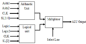
The block diagram of proposed ALU is shown in Fig.1 which consists of an arithmetic unit, logic unit and a multi- plexer. Arithmetic unit is designed to perform the arithmetic operations like addition, subtraction, multiplication and divi- sion. Logic unit is designed to perform the logic operations using basic logic gates with reversible logic. Multiplexer is used to select any one of the circuit operation either arithmetic or logic operation and directs the output of respective unit to the output terminals of ALU. The circuit design and imple- mentation of sub-blocks are described in detail below.
Fig. 1. Block Diagram of Proposed ALU
Reversible logic gate can be used to perform logical operations like AND, OR, NAND, NOR, Buffer, XOR, XNOR with high speed, less area and less complexity. In this logic at any instant of time one of the input acts as a control input and other two works as data input. The logic circuit computation using re- versible logic gate improves the efficiency of the circuit with low power dissipation.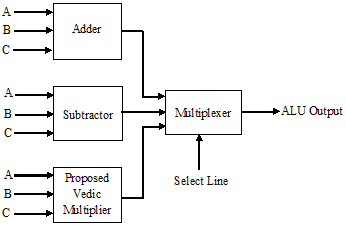
Fig. 2. Proposed Arithmetic Unit
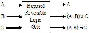
Fig. 3. Proposed Reversible Logic Gate
The logic blocks of arithmetic unit is designed using re- versible logic gates and Vedic multiplier which are used to reduce the power dissipation and transistor count of arithme- tic unit. The block diagram of arithmetic unit is shown in Fig.2. The reversible logic gate is employed to obtain the logic operation with low power dissipation.
The logic block of a proposed reversible logic gate is shown in Fig.3 in which the reversible logic gate accepts three inputs and provides three outputs. One to one mapping tech- nique is used in the reversible logic gate that helps to deter- mine the outputs from input and that outputs can be used to recover the inputs. It satisfies the demand of Landauer’s prin- ciple and C.H. Bennett rule that are defined for energy effi- ciency. The reversible gate can be used to perform all the logic gates with high speed and low area and power dissipation.
IJSER © 2015 http://www.ijser.org
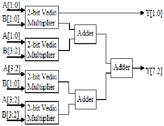
Fig. 4. Proposed 4-bit Vedic Multiplier
International Journal of Scientific & Engineering Research, Volume 6, Issue 2, February-2015 7
ISSN 2229-5518
Usually multipliers are implemented in the digital system using multiple number of adders and such a multipliers are implemented with the help of array and booths algorithms. But Vedic mathematics illustrates the multiplication operation very faster than other algorithms by reducing number of addi- tion. The reduced number of adders in Vedic multiplier mini- mizes the operating delay and area of device with less number of adders. For example consider a N × N multiplier, it may require N×(N-2) full adders, N half-adders and N×N AND gates to perform the multiplication. But Vedic multiplier re- quires only N¬2 gates and (N‒1) adders. Since the use of less number of adder Vedic multiplier occupy less area and con- sumes reduced power in logic implementation and operation respectively.
A proposed 4-bit Vedic multiplier is shown in Fig.4 in which the logic evaluation of multiplication process is per- formed using divide and conquer method. The logic multipli- cation of two 4-bit binary number with proposed Vedic multi- plier is described below. Let us assume the binary inputs are A4A3A2A1 and B4B3B2B1. The output expressions of pro- posed Vedic multiplier are
X0[3:0] = A[1:0] × B[1:0]
X1[3:0] = A[1:0] × B[3:2]
X2[3:0] = A[3:2] × B[1:0]
X3[3:0] = A[3:2] × B[3:2] (1)
Then the logic addition of multiplied terms are performed
as follows
Y[1:0] = X0[1:0]
Y[2] = X0[2] + X1[0] + X2[0] + 1’b0
Y[3] = X0[3] + X1[1] + X2[1] + 1’b0
Y[4] = X1[2] + X2[2] + X3[0]
Y[5] = X1[3] + X2[3] + X3[1]
Y[7:6] = X3[3:2] (2) In this proposed logic the logic addition is performed using reversible logic gates which is an energy efficient arithmetic
logic circuit in the digital system design.
The logic output of 4-bit Vedic multiplier is designed by
the combinations of 2-bit Vedic multipliers. The block diagram
of 2-bit Vedic multiplier is shown in Fig 5. It is implemented
using the adders and logic gates.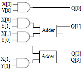
Fig. 5. Proposed 2-bit Vedic Multiplier
The block diagram of logic unit is shown in Fig.6 which is consisting of a reversible logic gate and a multiplexer. The logic outputs of reversible gate are selected by the multiplex- er. The energy efficient reversible logic gate is used to per- form the logic operations with reduced power dissipation and area.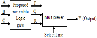
Fig. 6. Block diagram of Proposed Logical Unit
The proposed functional blocks of ALU circuit are implemented by using hardware description language. And the outputs are analyzed by comparing with the conventional architecture that results in the minimized power consumption and reduced area. All the presented high performance low power architecture outputs are implemented using Verilog Hardware Description Language (HDL) and synthesized in cadence RTL
compiler using TSMC 0.18μm CMOS technology library file.
The low power techniques are synthesized to observe the power and area of each technique separately. Also by employing the low power techniques in ALU architectures, we obtained the power and area of proposed processors. The area and power of proposed structures are compared with conventional structure that results in the reduced power consumption and area, increased performance.
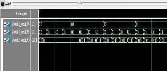
Fig. 7. Simulation result of Reversible Logic gate
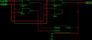
Fig. 8. Synthesized result of Reversible Logic gate
IJSER © 2015 http://www.ijser.org
International Journal of Scientific & Engineering Research, Volume 6, Issue 2, February-2015 8
ISSN 2229-5518
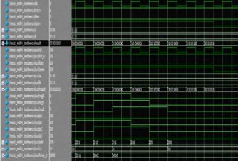
Fig. 9. Simulation result of 4-bit Vedic Multiplier
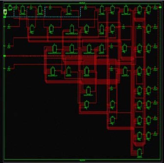
Fig. 10. Synthesized result of 4-bit Vedic Multiplier
The logic implementation of reversible logic gate is shown in Fig 7 and 8. The simulation output of reversible logic gate is shown in Fig 7. The synthesized RTL model of reversible logic gate is shown in Fig 8. The logic implementation of Vedic mul- tiplier with reversible logic gate is shown in Fig 9 and 10. The simulation output of Vedic multiplier is shown in Fig 9. The synthesized RTL model of Vedic multiplier is shown in Fig 10. The low power and area efficient logic blocks are integrated to implement ALU. The proposed logic blocks are implemented using Verilog HDL programming language, simulated and synthesized using Xilinx ISE 9.2i software.
integrated to construct architecture of ALU resulted that the power dissipation of proposed ALU unit is reduced when compared with the conventional unit. The use of less number of adders in the Vedic multiplier reduce the area and power dissipation of ALU system. The proposed logic blocks are im- plemented using Verilog HDL programming language, simu- lated and synthesized using Xilinx ISE 9.2i software. The syn- thesized output resulted that the proposed technique con- sumes the 35% of power, area of 23% less and the 17% of high- er performance compared to conventional ALU circuit.
[1] Mahapatro M, Panda, S.K. ; Satpathy, J. ; Saheel, M, “Design of Arithmetic Circuits Using Reversible Logic Gates and Power Dissipation Calculation”, Electronic System Design (ISED), IEEE 2010, pp.85-90.
[2] Maity M, Ghosal P, Das B, “Universal reversible logic gate design for low power computation at nano-scale” Microelectronics and Electronics (Pri- meAsia), IEEE 2012, pp.173-177.
[3] Bruce, J.W, Thornton, M.A, Shivakumaraiah, L, Kokate, P.S, “Efficient adder circuits based on a conservative reversible logic gate”, VLSI 2002, IEEE Pro- ceedings, pp.74-79.
[4] “Design of Arithmetic Circuits Using Reversible Logic Gates and Power
Dissipation Calculation” Wiley-IEEE Press eBook, 2011, pp. 417-443.
[5] Kumar U, Goud A.S, Radhika A, “FPGA implementation of high speed 8-bit Vedic multiplier using barrel shifter”, Energy Efficient Technologies for Sus- tainability (ICEETS), IEEE 2013, pp.14-17.
[6] Kunchigi V, Kulkarni L, Kulkarni S, “High speed and area efficient Vedic multiplier”, Devices, Circuits and Systems (ICDCS), IEEE-2012, pp.360-364.
[7] Rakshith T.R, Saligram, Rakshith, “Design of high speed low power multipli- er using Reversible logic: A Vedic mathematical approach”, ICCPCT, IEEE
2013, pp.775-781.
[8] Morrison M, Ranganathan N, “Design of a Reversible ALU Based on Novel
Programmable Reversible Logic Gate Structures”, VLSI, IEEE 2011, pp. 126-
131.
[9] Saligram, Rakshith T.R, “Towards the design of fault tolerant reversible cir- cuits components of ALU using new PCMF gate”, ICACCI, IEEE 2013, pp.862-867.
[10] Morrison M, Lewandowski M, Meana R, Ranganathan N, “Design of a novel
reversible ALU using an enhanced carry look- ahead adder”, Nanotechnolo- gy, IEEE 2011, pp.1436-1440.
[11] Senthil Sivakumar M, Banupriya M, “Low power high performance design consideration of CMOS domino logic for fast adders”, Journal of Scientific Theory and Methods, 2012, vol.12, pp.22-39.
[12] Jiaoyan Chen, Vasudevan D, Popovici E, Schellekens M, “Design of a Low Power, Sub-Threshold, Asynchronous Arithmetic Logic Unit Using a Bidirec- tional Adder”, Digital System Design (DSD), IEEE 2011, pp.301-308.
[13] Senthil Sivakumar M, Banupriya M, “Design Consideration of Dual Threshold Logic for High Performance and Ultralow Power Carry Look-Ahead Adder”, IJSER, vol.3, issue 6, June 2012, pp.1301-1306.
In this paper, the low power and high performance ALU circuit is implemented. The low power and area efficient logic blocks reversible logic based adder and Vedic multipliers are
IJSER © 2015 http://www.ijser.org