International Journal of Scientific & Engineering Research, Volume 6, Issue 4, April-2015 365
ISSN 2229-5518
Design and Verification of Efficient Majority Logic
Fault Detection and Correction for Memory
Applications
Harshitha B, Karthik M
Abstract— Memory is important for storing data and also to retrieve data in any digital circuit but the main problem is SEUs (Single Event Upsets). SEUs are the bigger concerns for memory applications as it alters the normal working of digital circuits and gives an error. This paper presents a fault detection and correction method which reduces access time when there is no error while reading data for difference- set cyclic codes with majority logic decoding as it can be applied to correct a large number of errors.
Index Terms— Bits, Cyclic-codes, Decoding, Encoding, Error, Fault, Majority-logic, Memory
—————————— ——————————
There has been a significant increase in memory failures which is a major reliability concern for applications [1]. Tech- nology scaling impact affects reliability of memory applica- tions like spacecraft, terrestrial environments and avionics electronics. There are two types of errors or failures.
1. Soft errors.
2. Hard errors.
Soft errors are not permanent and are due to upset of a semi-
conductor device. Hard errors are permanent and are due to
physical characteristics of the device [1].
Techniques to mitigate Soft Errors:
By far, the most effective method of dealing with soft errors in memory components is by employing additional circuitry for error detection and/or correction. In its simplest form, er- ror detection consists of adding a single bit to store the parity (odd or even) of each data word (regardless of word length). Whenever data are retrieved, a check is run comparing the parity of the stored data to its parity bit. If a single error has occurred, the check will reveal that the parity of the data does not match the parity bit. Thus, the parity system allows for the detection of a soft error for a minimal cost in terms of circuit complexity and memory width (only a single bit is added to each word). The two disadvantages of this system are that the detected error cannot be corrected and if a double error has occurred then the check will not reveal that anything is wrong since the parity will match. This is true for any even number of errors. For example, if the data were stored with odd parity, the first error changes the odd parity to even parity (detectable
————————————————
• Harshitha B, Assistant Professor, Dept. of ECE, B.M.S. College of Engi- neering, Bangalore, India – 560019
E-mail: harshithab.ece@bmsce.ac.in
• Karthik.M, M.Tech (Electronics), B.M.S. College of Engineering, Banga- lore, India – 560019
E-mail:karthik.raj016@gmail.com
ings, error detection and correction (EDAC) or error correction codes (ECC) are employed. Typically, error correction is achieved by adding extra bits to each data vector encoding the data so that the “information distance” between any two pos- sible data vectors is, at least, three.
Some commonly used Decoding types are techniques are:
• Triple modular redundancy (TMR)
• Error correction codes (ECCs)
TMR is a special case of the von Neumann method consisting
of three versions of the design in parallel, with a majority vot-
er selecting the correct output. As the method suggests, the
complexity overhead would be three times plus the complexi-
ty of the majority voter and thus increasing the power con- sumption. For memories, it turned out that ECC codes are the best way to mitigate memory soft errors [3]. For terrestrial radiation environments where there is a low soft error rate
(SER), codes like single error correction and double error de- tection (SEC-DED), are a good solution, due to their low en- coding and decoding complexity.
Among the ECC codes that meet the requirements of higher error correction capability and low decoding complexity, cy- clic codes have been identified as good candidates, due to their property of being majority logic (ML) decodable [6]. A subgroup of the low-density parity check (LDPC) codes, which belongs to the family of the ML decodable codes, has been researched in [7]-[9].
The main reason for using ML decoding is that it is very simple to implement and thus it is very practical and has low complexity. The drawback of ML decoding is that, for a code- word of certain bits, it takes as many cycles in the decoding process, posing a big impact on system performance [2]. This has motivated the use of a fault detector module [9].
error), but the second error changes the parity back to odd
(non detectable error) [3]. In order to address these shortcom-
IJSER © 2015 http://www.ijser.org
International Journal of Scientific & Engineering Research, Volume 6, Issue 4, April-2015 366
ISSN 2229-5518
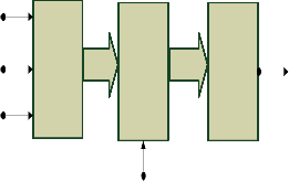
A general schematic of a memory system is depicted in Fig.1 for the usage of an encoder and decoder. Initially, the data words are encoded and then stored in the memory. When the memory is read, the codeword is then fed throught the decod- er before sent to the output for further processing. In this de- coding process, the data word is corrected from all bit-flips that it might have suffered while being stored in the memory.
Message Bits
M(x)
Message Bits
G1 G2
R0 + R0 +
Remainder R(x)
Gn-k-1
R0 +
GATE
R0
Messgae
Input M(x)
Feedback Before Shift
+
Clock (Clk) Reset
Encoder Memory Decoder
Read/ Write
M(x)
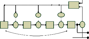
Fig.2. Cyclic Encoder Block Diagram
There are two ways for implementing decoder. The first one is called the type-1 ML decoder, which determines upon XOR combinations of the syndrome, which bits need to be corrected [4]. The second one is the type-2 ML decoder that calculates directly out of the codeword bits the information of correct-
Fig.1. Memory system schematic with Encoder & Decoder
In order to reduce complexity of the design and increase the computation time, we go for cyclic encoding. Cyclic codes form an important subclass of linear codes. These codes are attractive for two reasons: first, encoding and syndrome com- putation can be implemented easily by employing [4].
Shift registers with feedback connections (or linear sequen- tial circuits) and second, because they have considerable in- herent algebraic structure, it is possible to find various practi- cal methods for decoding them. If the components of an n- tuple v = (v0 , v1 . . . , vn-1 ) are cyclically shifted one place to the right, we obtain another n-tuple, v(1) = (vn-1 , v0 . . . , vn-2 ) which is called a cyclic shift to v. if the components of v are cyclically shifted I places to the right, the resultant n-tuple would be
v(i) = (vn-i , vn-i+1 , ....., vn-1 ,v0 , v1 .... , vn-i-1 )
Clearly, cyclically shifting v I places to the right is equiva- lent to cyclically shifting vn-i places to the left. An (n, k) linear code C is called a cyclic code if every cyclic shift of a code vec-
tor in C is also a code vector in C.
Consider D(x) as message bits and V(x) as code vector, G(x)
as generator polynomial. In (n,k) cyclic codes n represents
number of encoded bits and k represents message bits. n-k
represents remainder bits to form code vector.
Remainder bits R(x) can be obtained by dividing X(n-k) and![]()
M(x) by the generator polynomial G(x).
Remainder bits are combined with message bits to form code vector V(x) = R(x).M(x)
Fig.2. shows the general block diagram of cyclic encoder.
ness of the current bit under decoding [4]. Both are quite simi- lar but when it comes to implementation, the type-2 uses less area, as it does not calculate the syndrome as an intermediate step. Therefore, this paper focuses only on this one.
NORMAL ML DECODER:
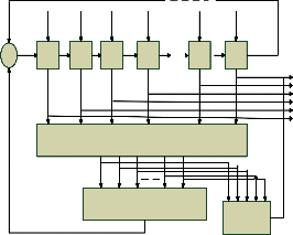
The ML decoder is a simple and powerful decoder, capable of correcting multiple random bit-flips depending on the number of parity check equations. It consists of four parts: 1) a cyclic shift register; 2) an XOR matrix; 3) a majority gate; and 4) an XOR for correcting the codeword bit under decoding as illus- trated in Fig.3.
The input signal is initially stored into the cyclicl shift regis- ter and shifted through all the taps. The intermediate values in each tap are then used to calculate the results {Aj} of the check sum equations from the XOR matrix. In the Nth cycle, the re- sult has reached the final tap, producing the output signal y (which is the decoded version of input x).
As stated before, input x might correspond to wrong data corrupted by a soft error. To handle this situation, the decoder would behave as follows. After the initial step, in which the codeword is loaded into the cyclic shift register, the decoding starts by calculating the parity check equations hardwired in the XOR matrix. The resulting sums {Aj} are then forwarded to the majority gate for evaluating its correctness. If the number of 1’s received in {Aj} is greater than the number of 0’s, that would mean that the current bit under decoding is wrong, and a signal to correct it would be triggered. Otherwise, the bit under decoding would be correct and no extra operations would be needed on it.
In the next step, the content of the registers are rotated and the above procedure is repeated until all N codeword bits have been processed. Finally, the parity check sums should be zero if the codeword has been correctly decoded. Further de- tails on how this algorithm works can be found in [2]. The whole algorithm is depicted in Fig.4. The previous algorithm needs as many cycles as the number of bits in the input signal, which is alsothe number of taps, N, in the decoder. This is a
IJSER © 2015 http://www.ijser.org
International Journal of Scientific & Engineering Research, Volume 6, Issue 4, April-2015 367
ISSN 2229-5518
big impact on the performance of the system, depending on the size of the code. For example, for a codeword of 73 bits, the decoding would take 73 cycles, which would be excessive for most applications.
lustrated in Fig.6 as: 1) the control unit which triggers a finish flag when no errors are detected after the third cycle and 2) the output tristate buffers. The output tristate buffers are al- ways in high impedence unless the control unit sends the fin- ish signal so that the current values of the shift register are forwarded to the output.
X[N-1]
X[N-2]
X[N-3]
X[N-4]
X[1]
X[0]
The control schematic is illustrated in Fig.7. The control
II
R R R R
XOR Matrix
Y[0] Y[1] Y[N-4]
unit manages the detection process. It uses a counter that counts up to three, which distinguishes the first three itera- tions of the ML decoding. In these first three iterations, the control unit evaluates {Aj} by combining them with the OR1 function. This value is fed into a three-stage register, which holds the results of the last three cycles. In the third cycle, the
B1 B2 B3
Bj-1 Bj
OR2 gate evaluates the content of the detection register. When the result is “0”, the FSM sends out the finish signal indicating
III
Majority Gate
that the processed word is error-free. In the other case, if the result is “1”, the ML decoding process runs until the end.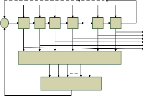
Fig.3. Schematic of an ML decoder
Load Cyclic Shift Register i=0
Evaluate
XOR-Matrix
i<=3
Load Detection Register
yes
Correct Bit Under Decoding
Majority Gate
# of ‘1’ > # of ‘0’
Cyclic Shift i++
I = N
NO
YES
END
NO
Correct Bit Under Decoding
Majority Gate
# of ‘1’ < # of ‘0’
Cyclic Shift i++
i = N
yes
YES
i=3 & Detection Register=”000"
YES
END
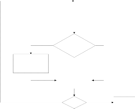
Fig.4. Flowchart of the ML algorithm
ADVANCED ML DECODER:
In general, the decoding algorithm is still the same as the one in the normal ML decoder version. The difference is that, instead of decoding all code word bits by processing the ML decoding during N cycles, the proposed method stops inter- mediately in the third cycle if the data read from the memory is error free, as illustrated in Fig.5.
If in the first three cycles of the decoding process, the eval- uation of the XOR matrix for all {Aj} is “0”, the code word is determined to be error free and forwarded directly to the out- put. If the {Aj} contain in any of the three cycles at least a “1”, the proposed method would continue the whole decoding process in order to eliminate the errors.
A detailed schematic of the proposed design is shown in Fig.6. The figure shows the basic ML decoder with an N-tap shift register, an XOR array to calculate the orthogonal parity check sums and a majority gate for deciding if the current bit under decoding needs to be inverted. Those components are the same as the ones for the plain ML decoder shown in Fig.3. The additional hardware to perform the error detection is il-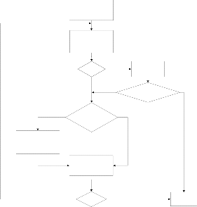
Fig.5. Flow diagram of the MLDD algorithm
This clearly provides a performance improvement respect to the traditional method. Most of the words would only take three cycles (five, if we consider the other two for in- put/output) and only those with errors (which should be a minority) would need to perform the whole decoding process.
IJSER © 2015 http://www.ijser.org
International Journal of Scientific & Engineering Research, Volume 6, Issue 4, April-
ISSN 2229-55X[1N8-1]
X[N-2]
X[N-3]
X[N-4]
X[1]
X[0]
R R R R
XOR Matrix
II
Y[0]
Y[1] Y[N-4] Y[N-3]
Y[N-2]
Y[N-1]
B1 B2 B3
Bj-1 Bj
Finish
Fig.9. ML decoder without error simulation output
Majority Gate
Control
I Unit
Fig.6. Schematic of MLDD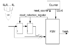
Fig.7. Schematic of the control unit
DATA ENCODER:
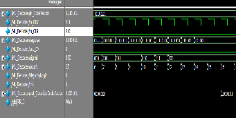
Encoding is done for the signal 101. The generated code vector is 1100101.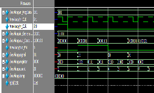
Fig.8. Cyclic encoder simulation output
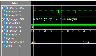
DATA ML DECODER:
Normal decoder requires N number of cycles to decode the message bits. For (7, 3) encoding it takes about 7 cycles to de- code the data from the memory. To load the shift register it takes first six cycles then from the seventh cycle decoding pro- cess starts for next 7 cycles (N bits).
Fig.10. ML decoder with error simulation output
MLD DECODER:
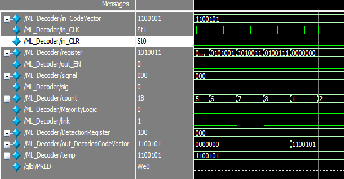
Fig.11. MLD decoder without error simulation output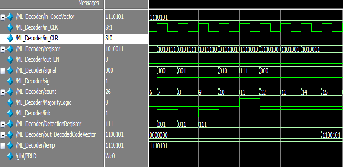
Fig.12. MLD decoder with error simulation output
In this paper, a fault-detection mechanism MLDD has been presented based on ML decoding using the DSCCs. One example codes were simulated and test results show that the proposed technique is able to detect bit-flips in the first three cycles of the
IJSER © 2015 http://www.ijser.org
International Journal of Scientific & Engineering Research, Volume 6, Issue 4, April-2015 369
ISSN 2229-5518
decoding process. This improves the performance of the design with respect to the traditional MLD approach. The MLDD error detector module has been designed in a way that is independent of the code size. This makes its overhead quite reduced compared with other traditional approaches such as the syndrome calcula- tion (SFD). The ML decoder circuitry is used here as a fault detec- tor so that read operations are accelerated with almost no addi- tional hardware cost. The results show that the properties of DSCC-LDPC enable efficient fault detection.
[1] C.W. Slayman, “Cache and memory error detection, correction, and reduction techniques for terrestrial servers and workstations”, IEEE Trans. Device Ma- ter. Vol 5, no. 3, pp. 397-404, Sep. 2005
[2] R.C. Baumann, “Radiation-induced soft errors in advanced semicon- ductor technologies”, IEEE Trans. Device Mater. Vol.5, no. 3, 301-316, Sep. 2005
[3] R.Naseer and J.Draper, “DEC ECC design to improve memory relia- bility in sub-100 nm technologies”, in Proc. IEEE ICECS, 2008, pp.
586-589
[4] S.Lin and D.J. Costello, Error Control Coding 2nd ed. Englewood
Cliffs, NJ: Prentice-Hall
[5] I.S.Reed, “A class of multiple-error correcting codes and the decod- ing scheme”, IRE Trans. Inf. Theory
[6] J.L. Massey Threshold Decoding. Cambridge, MA: MIT Press
[7] S.Ghosh and P.D.Lincoln, “Low-density parity check codes for error correction in nanoscale memory”, SRI Comput. Sci. Lab. Tech.
[8] B. Vasic and S.K.Chilappagari, “An information theoretical frame- work for analysis and design of nanoscale fault-tolerant memories based on low-density parity-check codes”, IEEE Trans. Circuits Syst.
[9] H.Naeimi and A.DeHon, “Fault secure encoder and decoder for Na-
noMemory applications”, IEEE Trans. Very Large Scale Integr.
IJSER © 2015 http://www.ijser.org