International Journal of Scientific & Engineering Research, Volume 5, Issue 12, December-2014 65
ISSN 2229-5518
Design and Implementation of DC- DC/AC Non- Inverting Cuk Converter using Sliding Mode Control
P.Nagalakshmi Kanna1, Dr.B.Meenakshi2 M.E, Ph.D
Abstract— In design of single stage Multi-Input DC-DC/AC Converters, the DC inputs are given to the Multi-Input converter. According to the pulse given, the convertor produces either DC output or AC output. This can be used for supplying power to DC or AC application. The outputs of the solar, Battery and wind energy sources are given as the inputs to the Multi Input Convertor (MIC). The magnitude of output voltage of MIC is increased by using Non-Inverting Cuk converter. There are many methods available to convert DC to AC (or) DC to DC. In this work both DC to DC and DC to AC conversion is done in the same system without including an additional devices. This will be more beneficiary in applications where uninterrupted AC or DC power supply is needed. Sliding Mode Control (SMC) technique is used to control the performance of the system. The proposed system is implemented in MATLAB/SimulinkTM platform and the output performances are analyzed.
Index Terms—Multi Input Converter, Sliding Mode Control, Pulse W idth Modulation, Multi Input Multi Output.
—————————— ——————————
1. INTRODUCTION
In recent years most electrical systems are supplied
by any one kind of energy source, like battery, wind or solar. Renewable energy sources will be of particular interest, as resources are further distributed to the power grid. There are many converters available such as Buck, Boost, Buck-Boost, and Cuk. MIC uses these types of converters to get multiple outputs. If any one of the input is not available remaining sources are used to supply the load, so entire distribution is not interrupted. Previously MICs are used to get either DC or AC from DC with additional device like inverter incase of getting AC Output and rectifier for DC output and also the usage of switches and diodes are more [1]-[3].
In a Multi Input Multi Output (MIMO) system multiple
inputs can be given, an inverter part is added to the converter to get AC output voltage but to get the DC output voltage ,the inverter part is disconnected from the system[2].A new topology is used in MIMO system , Multiple DC output is derived from Multiple DC input . Here the input and the output fall under the same category (DC to DC) [3].Using frequency isolation transformer the output will be regulated by means of feedback control that employs a PWM controller, where the control voltage is compared with the saw tooth waveform at switching frequency [4].
An extra pulsating voltage source cells or pulsating
current source cells are added to the Pulse converter for synthesizing an MIC. By introducing this, two families of MIC’s are generated [5].A new approach for electronics converters based on energy shaping is presented in [6]. Systematic

1. P.G. Student, Dept of Electrical & Electronics Engineering, Sri
Sairam Engineering College,Chennai, Tamil Nadu, India
2. Professor, Dept. of Electrical & Electronics Engineering, Sri
Sairam Engineering College,Chennai, Tamil Nadu, India
approach based on graft scheme foe modeling the Cuk and other converter [7]. The small signal models of cuk converter and other converters deal with h parameter for buck converter and g parameter for a boost converter [8].
In this work by giving proper gate pulses to the converter, DC output as well as AC output is obtained from DC inputs. The DC inputs are fed to the Non- Inverting Cuk Converter which has a bidirectional port at the central part. Here Sliding Mode Control (SMC) is employed to give pulse for the respective switches. To reduce the switching complexity in this proposed system SMC is designed for converter1. Converter2 is getting signals from the SMC of converter1.Thus the SMC is employed to control the pulses of both the converters. Using this control value of input voltages is varied until the output voltage and current across the load is constant.
2. LITERATURE REVIEW
Many research works were proposed based on Dc- DC converter and DC-AC converter for renewable energy system.
Bryan et al (2003) proposed a new topology for multiple energy source conversion [1]. This topology is capable of interfacing sources of different voltage-current characteristics to a common load. In MIBB (Multi Input Buck- Boost Converter), there are N- input voltages and N-input currents interfaced through a forward-conducting-bidirectional- blocking (FCBB) switch. In the case of MIBB lot of versatility in the input sources. It may be an unreasonable constraint to impose a minimum inductor current (in order to assure continuity) when trying to optimize the contributions from all sources connected. In this topology, DC–DC converter is capable of supporting multiple inputs and assures for achieving diversification of multiple energy sources. Idealized equations were used for the converter as an aid to design and a basis for control development.
IJSER © 2014 http://www.ijser.org
International Journal of Scientific & Engineering Research, Volume 5, Issue 12, December-2014 66
ISSN 2229-5518
Tao et al (2006) discussed about a family of multiport bidirectional DC–DC converters [3] .This topology shows a combination of DC-link and magnetic coupling and also the control and power management of the converter by a single digital processor. A phase shift and/or PWM generator is employed to generate phase-shifted square waves (PSSW) and Pulse-Width Modulation (PWM) control signals that control the transformer coupled switching cell and the DC- linked switching cells, respectively. The centralized control eliminates complicated communication structures that would be necessary in the conventional structure based on separate conversion stages. This Multi port converter control strategy based on classical control theory is showing a multiple PID loop structure.
Yuan-Chuan Liu et al (2009) proposed a general approach for developing multi-input converters [5]. The derived MICs can deliver power from all of the input sources to the load either individually or simultaneously. In this topology, PWM converters’ synthesizing an MIC is inspired by adding an extra pulsating voltage or current source to a PWM converter with appropriate connection. The output portion of the PWM converters sees a high-frequency pulse-train voltage or current waveform from the input portion or the energy buffer portion. By filtering out this high-frequency pulse-train voltage or current waveform with the output portion, a dc voltage or current can be obtained. The pulsating voltage source cells (PVSCs) and the pulsating current source cells (PCSCs) characteristics are used to synthesizing MICs.
Saeed Danyali et al (2014) proposed a new extendable multi input DC to DC and DC to AC converter for boost converter [12]. This paper describes about the single power switch of each unidirectional boost converter that is controlled to regulate the dc power of its corresponding input source, while in the central part of converter both upper and lower power switches of the bidirectional boost converters are complementary switched to produce their corresponding output reference voltages of converter. This paper concentrates pole placement approach and system stability using small signal model.
In this proposed System, the boost converter [12] is
replaced with Non inverting cuk converter and switching pulses of this topology is based on SMC. Here the usage of additional devices like inverter, transformer and output filters are eliminated. The performance of the proposed topology is discussed below.
3. PROPOSED CONVERTER AND OPERATION MODES
The Proposed Structure of MIC is shown in Fig 1. It
consists of two unidirectional Non-Inverting Cuk converters are connected to the bidirectional port which is in the middle part of the proposed system and it is also connected to the load. The Non- Inverting Cuk converter is similar to the Cuk converter, but the output of the converter is positive whereas the Cuk converter output is negative.
In this work three inputs are chosen. The Renewable Energy sources(Solar, Wind, Fuel, etc.,) outputs are given as the inputs to the converter1 and converter2 which are connected in parallel shown in Fig.2.
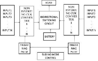
The third input source is Battery which is used to store energy during the conversion and act as energy source if any one of the sources is not available. Thus the load can get a continuous supply. Circuit diagram of the proposed system is shown in Fig.2.
Fig .1 Block Diagram of the proposed topology.
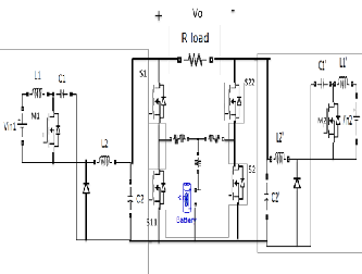
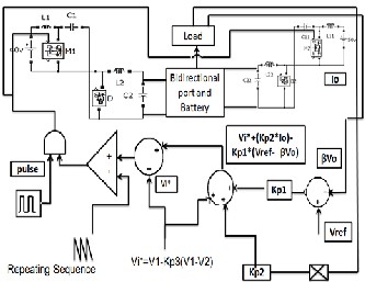
Fig.2 Circuit Diagram of the proposed system.
This proposed system has two output modes that are DC and AC. For both the operation, inputs are DC voltages. While getting DC to DC mode, the inputs are given to both the converters and the converter’s output voltages are fed to the load. For getting AC output, the input of the converter1 is given in 180 degree phase shift to the converter2. That is two inputs are made as biased input and then it is applied to the converters. Switching pulses are given with the help of SMC. In both the modes SMC is designed for converter1 and converter2 getting pulses from this SMC. Due to the structure of this proposed system there is no need for an output filter arrangement. The switches used for this topology are M1,S1,S2,S11,S22,M2.The duty ratio for this topology is d1,d2,d3…..d6.
4. CONVERTER MODE
A Non-Inverting cuk converter contains input voltage
IJSER © 2014 http://www.ijser.org
International Journal of Scientific & Engineering Research, Volume 5, Issue 12, December-2014 67
ISSN 2229-5518
source (V),MOSFET Switch(M),an anti parallel diode d, a
Freewheeling diode(D),a capacitor C1 for transferring energy
C. Advantages of Proposed Converter
and capacitor C2 for storing the energy ,two inductors L1 and• This circuit has a very low output current ripple due to the
L2,load resistor R. Let V1, V2 are voltage across the
capacitors C1 and C2 respectively.
The circuit setup is like a combination of the buck and boost converters. In Normal Cuk converter the circuit delivers an inverted output. But here the output is positive range. Virtually all of the output current passes through C1, and as ripple current. So C1 is usually a large electrolytic capacito•r
with a high ripple current rating and low ESR (equivalent
series resistance), to minimize losses. The main difference between the proposed converter and the other converters is
presence of L2 in the output circuit, similar to the Buck regulator. It also has a very low ripple current in the input circuit due to the presence of L1, similar to the Boost regulator. A further advantage is that only one switching device is required, with no base drive coupling problems as in the bridge and half-bridge circuits.
Another advantage of this converter is its capacitive isolation; the failure of the switching transistor will short the input and does not affect the output.
that here capacitor is used as the energy storing element.
• The two inductors L1 and L2 can be coupled together on one
µ is SMC signal applied at the gate of M. When µ is 1,
core.
the circuit is in charging mode. When µ is 0, the circuit is i • The converter can both Boost and Buck the output voltage.
discharging mode. Here the operation of converter divided into two modes. The operation of Switch On and Off state of the Non -Inverting Cuk Converter is shown in fig:3 and fig:4 respectively.
A. Switch Is On
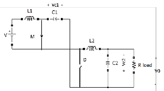
When MOSFET switch is turned on, the current through L1 rises. And at the same time the voltage of C1 reverse biases diode D and turn it off. The capacitor C1 discharges its energy to the circuit C1-C2-load-L2.
Fig.3 ON State of Non-Inverting Cuk Converter
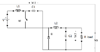
B. Switch Is Off
When MOSFET switch is turned off . The capacitor will start to charge from input supply Vs and the energy stored in the inductor transferred to the load. The capacitor C1 is the medium for transferring energy from source to load.
Performance equations of proposed converter are given
below:
D. DC TO DC MODE
The Voltage across the converter1 (Vc1)and converter2 (Vc2)are
V1=Vc1; V2=Vc2; (1) Voltage across the load=V0
V0 =V1-V2 (2) The power consumed by load is given below
Po=V0 I0 (3) Where RLoad = resistive load
Vc1=Voltage across converter1
Vc2=Voltage across converter2
V0 =Output voltage
I0 =Output current
I0 =(V1-V2)/RLoad (4) P0 =(V12+V22+2V1V2)/RLoad (5)
The Powers across the converter1 and converter2 are,
Po1 =Vc1*I0
Po2 = -Vc2*I0
P0 =P01 -P02 ( 6)
E. DC-AC MODE
The DC inputs which are given to the two converters are in 180 degree phase shift, and then the output is an AC Mode.
The voltage and current across the load are
V1 (t) = Vdc + Vm /2 sinωt
V2 (t) = Vdc -Vm /2 sinωt
V0 (t) =V1 (t)-V2 (t) =Vm Sinωt (7)
Where,
Vdc= DC bias value of the converter output voltages. Vm, Im =Converter output voltage and current peak. V0 ,I0 ,P0 =converter output voltage, current, power.
.
Fig.4 OFF State of Non-Inverting Cuk Converter
I0 (t) =Im Sinωt (8) Im =Vm /RLoad (9)
The Power across the load
P0 =V0 *I0 (10) P0 =P01 -P02 (11)
The output power across the converter1 and converter2
P01 =V1 (t)*I1 (t) (12) P02 =V1 (t)*I2 (t) (13)
IJSER © 2014 http://www.ijser.org
International Journal of Scientific & Engineering Research, Volume 5, Issue 12, December-2014 68
ISSN 2229-5518
Fig.5 Sliding mode controller for Non-Inverting Cuk Converter.
5. CONTROL TECHNIQUES USED FOR CONVERTERS
There are so many controllers are used to control the converters like P,PI and PID. The proposed system deals with non linear control methods which are suitable for higher order system converters. Buck & Boost converters are second order system whereas the proposed converter has fourth order derivatives.
A. Non-Linear Control Methods
The subject of non linear control deals with the analysis and design of Non-linear control systems. In the design of a non linear control, a Non linear system to be controlled and certain specifications of the closed-loop system meets the desired characteristics. Several tools are available for the analysis of the non linear systems. The following methods are used for non linear control.
• The describing function concept
• The piece wise linear approximation
• The phase plane
• The Lyapunov’s stability criterion
• Popov’s method and
• The Sliding Mode Control (SMC)
The proposed topology considers the sliding mode control which is one of the non- linear control methods which are mentioned above.
B. Sliding Mode Control
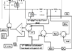
In the formulation of any practical control problem, there will be a mathematical model for the control design. These discrepancies arise from unknown external disturbances, plant parameters and parasitic/ unbalanced dynamics. Designing the control laws that provide the desired performance of the closed-loop system in the presence of these disturbances/uncertainties is a very challenging task. This has led to the intense development of the control robust control methods which are supposed to solve this problem. One particular approach to the robust controller design is the sliding mode control (SMC) technique. The SMC of Non- Inverting Cuk Converter is shown in Fig.5
C. Sliding Mode Control For Non- Inverting Cuk
Converter Dc-Dc Mode
Using SMC the output voltage & output current are maintained constant for a particular region even though the input voltages are changed. In DC-DC mode, the SMC has following process. The output of load voltage is compared with a constant reference value Vref, then the resulted error value (Vref-βVo) is compared with the output current (Io) & difference between the input voltages of the two converters (Vi*). Finally this output is compared with a carrier signal (ramp signal) and thus PWM signal generated then it is given as a gate pulse to converter1. This gate pulse is also given to the converter 2 which is connected parallel to the converter1.
D. Sliding Mode Control for Non-Inverting Cuk Converter
DC-AC Mode:
In this mode the output of the load is an AC Mode. Here the SMC is taken as reference value as DC voltage. When the reference DC Voltage (Vref) is compared with respect to the AC voltage, it becomes complicated while using SMC. To reduce the complication, that SMC output AC voltage is converted into DC by using a rectifier in SMC as shown in Fig.8. Now this output is compared with reference voltage Vref. Then the resulted error value is compared with the output current(Io) and the difference between the two converter input voltages Vi*.Finally it is compared with the carrier signal(ramp),then the PWM signal is generated and then this pulse is given to the converter1,This signal is also given to converter2 through NOT gate. Here both the converters are operated in 180 degree phase shift.
6. SIMULATION RESULTS
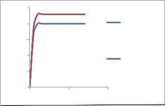
In order to verify the proposed converter performance, a low power three-input Non Inverting Cuk converter is designed as shown in Figs. 5 and 9. The proposed control scheme is SMC. Two different dc voltage sources of Vin1 = 40 V and Vin2 = 50 V, with the maximum deliverable voltage and current are shown in fig 7 & 8 and fig
10 &11.3A, the proposed parallel converters are utilized as the
converter input sources. Moreover, a 20Vbattery is employed in this prototype as the ESS. In order to validate practical performances of the proposed converter, All the experimental figures have been captured with the same scale.
Simulation block diagram of DC-DC and DC-AC modes are shown in Fig.6 and Fig.9 respectively. Both the Modes have same input voltages and the simulation is done using MATLAB. The Simulation results of output voltage and current across the load in both DC-DC modes are shown in Fig.7 and Fig.8 respectively. Similarly the output voltage and output current across the load in DC-AC modes are shown Fig.10 and Fig.11 respectively.
IJSER © 2014 http://www.ijser.org
International Journal of Scientific & Engineering Research, Volume 5, Issue 12, December-2014 69
ISSN 2229-5518
SIMULATION BLOCK DIAGRAM FOR DC-AC MODE
Fig.6 Simulation Block For DC-DC Mode
SIMULATION RESULTS FOR DC-DC MODE
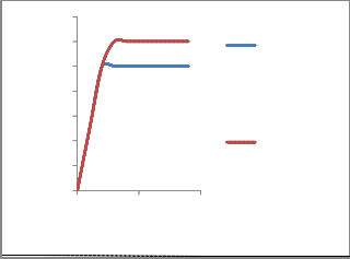
A. Output Voltage Vs Time
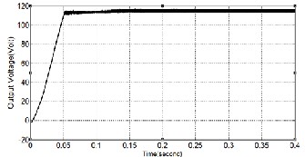
Fig.7 Output Voltage for the Proposed System in DC-DC Mode
B. Output Current Vs Time
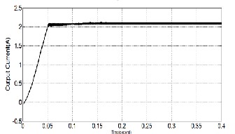
Fig.8 Output Current for the Proposed System in DC-DC Mode
Fig.9 Simulation block diagrm of DC-AC Mode
SIMULATION RESULTS FOR DC-AC MODE
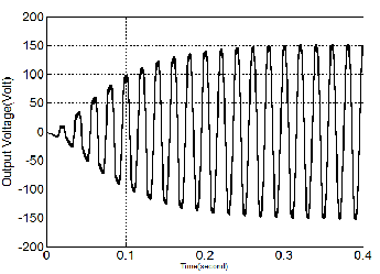
A. Output Voltage Vs Time
Fig.10 Output Voltage for the Proposed System in DC-AC Mode.
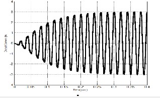
B. Output Current Vs Time:
IJSER © 2014 http://www.ijser.org
International Journal of Scientific & Engineering Research, Volume 5, Issue 12, December-2014 70
ISSN 2229-5518
Fig.11 Output Current for the Proposed System in DC-AC Mode.
VIII.COMPARISION OF OUTPUT VOLTAGE AND OUTPUT CURRENT BETWEEN BOOST AND NON-INVERTING CUK CONVERTER
140
2.5
2
1.5
1
0.5
0
0 0.5 1
boost converterO/P current
NonInverting Cuk converterO/P Current
120
100
80
60
Boost converter output voltage
Time(sec)
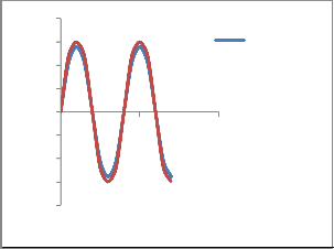
Fig.14 Output currents for DC-DC Mode.
4
40
20
0
0 0.5 1
Time(sec)
NonInverting
Cuk converter Output voltage
3 Boost
2 converter
Output
1 current
0
-1 0 0.5 1 NonInvertin
-2 g Cuk
-3 converter
Output
200
Fig.12 Output voltages for DC-DC Mode.
-4
Time(sec)
Current
150
100
50
0
-50
-100
-150
-200
0 0.5 1
Time(sec)
boost converter Output voltage
NonInverting Cuk converterOut put voltage
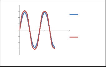
Fig.15 Output Currents for DC-AC Mode.
The comparison between Output voltage with respect to Time in DC-DC Mode and DC-AC mode is shown in Fig.12 & Fig.13 respectively. The input voltage of converter1 is set as
40V& converter2 is set as 50V.For DC-DC Mode the output of
the boost converter which is presented in [12] as 100v.The proposed converter output is 118V.In DC-AC Mode the Output voltage of the boost converter [12] is 140V.The proposed system output voltage as 150V.In both DC-DC and DC-AC Modes, the output voltage of the proposed converter is higher than the boost converter. Similarly the output current is compared with respect to time for DC-DC and DC-AC modes
Fig.13 Output voltages for DC-AC Mode.
are shown in Fig.14and Fig.15 respectively. Fig.14 represents
the output current Vs time in DC-DC Mode for the boost converter as 2A and the proposed converter as 2.3A.Likewise Fig.15 represents the output current Vs time in DC-AC Mode for the boost converter as 2.7A and the proposed converter as
3A. The comparisons between these two topologies are shown in Table I.
Input Voltage: Vin1=40V; Vin2=50V; RLoad =50Ω
TABLE I
Converter Topology | Modes | Output Voltage | Output Current |
IJSER © 2014 http://www.ijser.org
International Journal of Scientific & Engineering Research, Volume 5, Issue 12, December-2014 71
ISSN 2229-5518
three phase grid network with multiple inputs and SMC is designed for both sides of the converters.
Table I Comparison between converter Topologies.
A Non-Inverting Cuk converter is a combination of buck and boost converter, so that it can boost an input voltage to a higher voltage level than the input and can also cut the voltage down to any required level whereas the buck and the boost can step down and step up the voltage respectively only. Although a buck-boost converter can do the same thing, proposed converter is less complex than a buck-boost converter in terms of practical implementation. For constructing a buck-boost converter the switch has to be placed in series with the source. Placing the switch in series adds the complexity of proper grounding. And thus the use of separate opto-coupler circuit to isolate the ground of the PWM and converter, which makes the overall circuit much more complicated. Whereas the switch position in proposed converter is simple as the ground position of the source and the switch are same. No filter arrangement is needed here, because the proposed converter has a filter arrangement in its output side has filter arrangement itself. The output filter inductor is smaller for the proposed converter though it requires two inductors. The first inductor is basically for input current filtering. Due to this the outputs waveform has fewer distortions. These features are used to give higher magnitude with less distortion of output voltage and current.
7. CONCLUSION
In this paper the non inverting cuk converter is implemented to operate in both DC and AC modes and it also compared with the boost converter and the analyses are made. Here SMC is designed for one side of the converter part. The SMC can be seen as an effective tool for controlling the switch mode power supply and the system behavior, also it can force the converter to stay in the stable mode due to large line and load variation. The SMC is an efficient and easy control algorithm that could be implemented in MatLab/SimulinkTM and is gaining increasing importance as a control design tool in MatLab/SimulinkTM for the robust control of linear and non- linear systems .This Non Inverting Cuk Converter does not require an additional filter arrangement in the output side because this converter has filter arrangement built itself and this converter is also operated in discontinuous voltage mode also. Simulation results show all the converter capabilities such as low-current ripples for input dc sources, autonomous battery charging/discharging, and producing high-quality DC or AC output voltages.
In Future the proposed system can be implemented for
8.REFERENCES
[1]. Bryan G. Dobbs” A Multiple-input Dc-Dc converter topology,” IEEE Trans. Power Electron., Vol24, No.3, Mar.2009, pp.862-868.
[2]. A. Sudharshan, M.Yohan,” A Hybrid Wind-Solar Energy System Using Cuk-Sepic Fused Converter”, Int. Journal of Engineering Research and application, Vol. 3, No.6, pp.287-
293,Nov 2013.
[3]. H. Tao, A. Kotsopoulos, J. L. Durate, and M.A.M. Hendrix,” Family of multiport bidirectional Dc-Dc converters,” in Proc.IEE Elect. Power Appl., Apr.2006, pp.
451-458.
[4]. Kavya Shree G V, Eranna & K Chandra Mohan Reddy,” An Isolated Cuk Converter with Multiple Outputs Using PWM Controller” ITSI Transactions on Electrical and Electronics Engineering (ITSI-TEEE),Vol1,Issue 2,2013,pp-
2320 – 8945.
[5]. Yuan-Chuan Liu and Yaow-Ming Chen,” A Systematic
Approach to Synthesizing Multi-Input DC–DC Converters” IEEE Trans. Power Electron., Vol.24, No.1
,Jan.2009,pp.116-127.
[6]. ]. K. M. Smith, and K. Y. Ma Smedley, “Properties and synthesis of passive lossless soft-switching PWM converters,” IEEETrans. Power Electron,. Vol. 14, No. 5, pp. 890-899, Sept. 1999.
[7]. T. F. Wu, and Y. K. Chen, “A systematic and unified approach to modeling PWM DC/DC converters based on the graft scheme,” IEEE Trans. Ind. Electron., Vol. 45, No.
1, pp. 581-593, Feb. 1998.
[8]. T. F. Wu, and Y. K. Chen, “Modeling PWM DC/DC converters out of basic converter units,” IEEE Trans. Power Electron ,Vol. 13, No. 5, pp. 870-881, Sept. 1998.
[9]. Y. M. Chen, Y. C. Liu, S. C. Hung, and C. S. Cheng,
“Multi-input inverter for grid-connected hybrid PV/Wind power system,” IEEE Trans. Power Electron., Vol. 22, No.
3, pp. 1070–1077, May 2007.
[10]. L.Yan, R.Xinbo, Y.Dongsheng, L.Fuxin, and C.K. Tse,
”Synthesis of multiple-input Dc/DC Converters ,” IEEE Trans. Power Electron., Vol.25,No.9, Sep.2010,pp.2372-
2385.
[11]. A. Kwasinski, “Identification of feasible topologies for
multiple-input DC–DC converters,” IEEE Trans. Power
Electron., Vol. 24, No. 3, pp. 856– 861, Mar. 2010.
[12]. Saeed Danyali, Seyed Hossein Hosseini, and Gevorg B. Gharehpetian,”New Extendable Single Stage Multi input Dc-Dc/Ac converter,” IEEE Trans. Power Electron., Vol.
29, No. 2, pp. 775–787, Feb 2014.
IJSER © 2014 http://www.ijser.org
International Journal of Scientific & Engineering Research, Volume 5, Issue 12, December-2014 72
ISSN 2229-5518

IJSER © 2014 http://www.ijser.org