The research paper published by IJSER journal is about Design and Analysis of Pulse width Modulator (PWM) using Current Comparator 1
ISSN 2229-5518
Design and Analysis of Pulse width Modulator
(PWM) using Current Comparator
Rockey Choudhary, Monika Bhardwaj, Prof. B. P Singh
Abstract— This paper presents the new design of a simple pulse width modulator. The circuit principle is based on uniform sampling method known as uniform sampling PW M signal (UPW M) with a current comparator. The proposed scheme is simpler than the existing PW M methods and the duty factor linearly depend upon modulating signal. Another advantage is that the circuit is suitabl e for IC implementation. The simulating and experimental results are shown in this paper. It is suitable for high power applications as well as ordinary low power use.W hile possessing important advantages. Pulse-width (PW ) modulation has been widely used to convert analog (or multibit digital) signals to binary streams. The average power consumption is about 9.33mW under the implementation of TSMC 0.35μm CMOS process with 1.8V power supply.
Index Terms— Current Comparator, Current mode circuits, CMOS integrated circuits, Pulse-width modulation (PW M), Sample & Hold circuit, Triangular wave generator, Operational Amplifier..
—————————— ——————————
1 INTRODUCTION
ulse Width Modulation, is a method of controlling the amount of power to a load
without having to dissipate any power in the load
driver. Pulse-width modulation is a widely used technique of communication system, power management integrated circuit and signal processing units. The voltage-mode comparator is the most critical component of pulse-width modulator which dominates the accuracy of modulation process. However, voltage- mode comparator encounters several great difficulties including operational frequency, power consumption and input offset voltage. The current-mode comparator therefore has been attracted considerable attention as it is more easily to achieve design requirements than voltage-mode circuits. With respect to application of pulse-width modulation, input impedance of current comparator is the most important specification than operational frequency, power consumption and other specifications. The lower input impedance enhances the transformation efficiency of the signal and increases the accuracy of modulation process as well.
The PWM is widely used in many fields such as
communication, electronic control, power
electronic control and measurement circuits. It is currently realised in integrated circuits (ICs) form and that make it convenient to utilize. Some simple PWM using relaxation oscillator have been proposed [1,2]. Although its scheme is relatively
simpler but its duty factor does not linearly vary with modulating signal.
This paper proposed a simple PWM based on
uniform sampling method which can be realised in IC form. Its major advantage is that not only it can generate accuracy PWM signal with widely operating frequency but also its scheme is simpler than conventional PWM IC form. The simulation and experimental results are found to agree well with our anticipation.
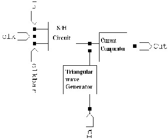
Fig 1 Block diagram of Pulse-width modulator
This paper is organized in four sections. Section 2 describes the principle of operation of proposed circuit. And the scheme of PWM signals generation and signal forms are also described in this section.
IJSER © 2012
http://www.ijser.org
The research paper published by IJSER journal is about Design and Analysis of Pulse width Modulator (PWM) using Current Comparator 2
ISSN 2229-5518
and also shows the circuits description ,which are used in proposed PWM. Section 3 shows the
simulation results and section 4 describes the conclusion respectively.
2 PULSE WIDTH MODULATION
2.1 PRINCIPLE OF OPERATION
Ordinarily the PWM signal can be classified into two forms [3]. One is PWM signal generated by natural sampling method which is called as natural sampling PWM signal (NPWM), another is PWM signal produced by uniform sampling method known as uniform sampling PWM signal (UPWM). Its scheme of generation PWM signals forms are shown in Fig 2 and Fig3 respectively.
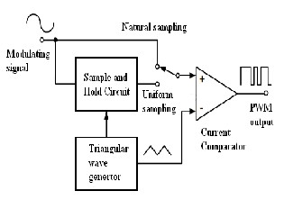
Fig.2 PW M Signal Generation
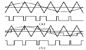
Fig. 3. The PW M Signal Forms
(a) Natural Sampling PW M Signal (b) Uniform
Sampling PW M Signal
For triangular carrier signal,it has two forms which
the first is sawtooth signal known as ‘single sided’ signal because only a single edge of the PWM waveform is modulated .Another is triangular signal called ‘double sided’ signal [4,5]. For the proposed method UPWM signal will be introduced and we can also use the NPWM signal in the proposed PWM.
The proposed PWM is schematically depicted in
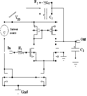
Fig1. If we assumed that sine wave signal is modulating signal, and triangular wave is carrier signal. Then PWM output signal is generated by comparing the output of sample and hold circuit and the carrier signal. We used a balanced low input impedance continuous-time CMOS current comparator for accurately performing pulse-width modulation.
2.2 CIRCUIT IMPLEMENTATION
2.2.1 CURRENT COMPARATOR
Current comparators are very important for analog circuit design because of their low power consumption, minimum size transistors, high speed, small chip area and many signal sources of sensors are current based.
The current comparator is applied to distinguish signals between two terminals with varied current in many applications. For instance, in a multimedia system, we use comparator as a pulse-width modulator to modulate audio signal by a reference carrier signal. In practice, a subtraction circuit always has to be included and this circuit will consume additional power and increases the time delay. Thus, to be complete we need to consider the CMOS current comparators with the current subtraction circuit. This is illustrated in Fig. 4. It consists of two cascode current mirrors and several voltage amplifiers. A NMOS cascode current mirror (M1 – M2) is added to the input to replicate the input current Iin. It drives a PMOS active current-source load (M5-M8) to convert the current difference between Iin and Iref CMOS complementary amplifier (M9 –M12) together with
the inverting amplifier
IJSER © 2012
http://www.ijser.org
The research paper published by IJSER journal is about Design and Analysis of Pulse width Modulator (PWM) using Current Comparator 3
ISSN 2229-5518
(M13 and M14) and two resistive-load amplifiers (M15 and M16; M17 and M18) act as the two gain stages. The last three CMOS inverters (M19 –M24) will be used to generate the rail-to-rail voltage.
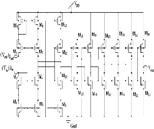
Fig. 4 Schematic of current comparator.
In our design, we connect the output of the
complementary amplifier (M9 – M12) to the output of the cascode current mirror in order to generate negative feedback which lowers the output impedance of current mirror, thereby increasing the response speed at low input currents.
Although the power dissipation of this CMOS
current Comparator is comparable with those found in [8],[9] (it should be pointed out that the power dissipation computed for the other circuits do not included the contribution from the subtraction circuit and the values will appear smaller).
Since the new CMOS current comparator includes
a subtraction circuit, extra time is needed to respond to the input current. For a more accurate comparison, we simulated the new CMOS current comparator without the subtraction circuit.
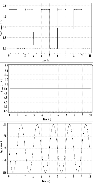
Fig.5 Transient waveforms of current comparator.
To verify the circuit performance, circuit has been simulated using the TSMC 0.35μm CMOS process and 1.8V voltage supply. It should be noted that while the input currents listed in [7-9] left out the current subtraction circuit, in our present design a subtraction circuit and an amplifier have been added. For convenience, we refer to the difference between Iref and Iin as the ‚input current‛. It is necessary to reduce the power dissipation so as to be compatible with PWM, the reference current Iref has been set to be 5μA. In our simulations, Iref
and Iin are implemented by Idc and sinusoidal
IJSER © 2012
http://www.ijser.org
The research paper published by IJSER journal is about Design and Analysis of Pulse width Modulator (PWM) using Current Comparator 4
ISSN 2229-5518
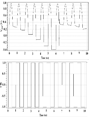
input current, respectively. We simulated this current comparator at the input current value ±1A. The result is shown in Fig. 5.
2.2.2 SAMPLE AND HOLD CIRCUIT
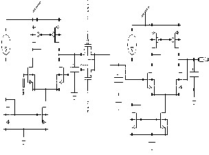
The sample-and-hold is the most basic and ubiquitous switched-capacitor building block. Before a signal is processed by a discrete-time system, it must be sampled and stored. This often greatly relaxes the bandwidth requirements of following circuitry which now can work with a DC voltage. A sample-and hold circuit is used to convert a time-continuous signal into a discrete- time signal at a pre-defined sampling rate [10]. The operation cycle of the sample-and-hold circuit is divided into two distinct phases, which are indicated by its name: the sampling phase and the holding phase. In the sampling phase the analog signal is sampled and in the holding phase the sampled signal must be fixed until the next sampling phase. At this point. the time continuous
signal is converted to discrete time. 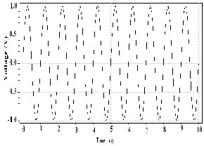
Fig.7.Transient waveforms of sample and hold circuit
Fig.6 Schematic of sample and hold circuit.
A good model for the sample-and-hold circuit, on
the sampling phase is an operational amplifier in a unity gain configuration [11]. The original analog signal is applied to the input. and at the output there is the load capacitor as shown in Fig.6. For the holding phase it is also convenient to use an operational amplifier buffer in a unity gain configuration. Now the load capacitor is placed at the input. since it stores the instantaneous value of
the analog signal.. The signal was stored at the
IJSER © 2012
http://www.ijser.org
The research paper published by IJSER journal is about Design and Analysis of Pulse width Modulator (PWM) using Current Comparator 5
ISSN 2229-5518
transition from the sampling to the holding phase. Therefore at the output there is a discrete-time signal that is the sampled version of the analog input signal. The transient behavior of the sample and hold circuit is shown in Fig.7
2.2.3 TRIANGULAR WAVE GENERATOR
We know that the integrator output waveform will
be triangular if the input to it is a square-wave. It means that a triangular-wave generator can be formed with an integrator by applying the square wave at the input of the integrator, as illustrated in Fig8. This circuit needs an op-amp, two capacitors, and two resistors. When the square wave is applied to the input of integrator, it drives the integrator which produces a triangular output waveform. The rectangular-wave swings between
+1V and -1V is applied to the input. The triangular- waveform has the same period and frequency as the square-waveform. Peak to-peak value of output triangular-waveform can be obtained from the following equation.
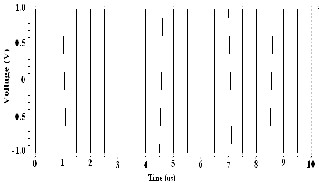
Fig.9 Transient waveforms of Triangular wave generator
The input of integrator is a square wave and its output is a triangular waveform, the output of integrator will be triangular wave only when R C > T/ 2 where T is the ( period of square wave. As a general rule, RC should be equal to T. Since the frequency of the triangular-wave generator like any other oscillator, is limited by the op-amp slew- rate, a high slew rate op-amp, like LM 301, should be used for the generation of relatively higher frequency waveforms. The transient waveform of triangular wave generator is shown in Fig9.
3 SIMULATION RESULTS
In this section, we demonstrate the practicability of proposed design Pulse-width Modulator through implementing circuits of Fig.1 by TSMC 0.35 µm CMOS process. The experiment results are reported in Fig.10 to Fig 12 which shows the input
and output waveform of Pulse-width modulator
Fig.8 Schematic of Triangular wave generator.
IJSER © 2012
http://www.ijser.org
The research paper published by IJSER journal is about Design and Analysis of Pulse width Modulator (PWM) using Current Comparator 6
ISSN 2229-5518
and average power compared to that of prior
work.
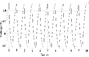
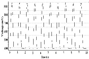
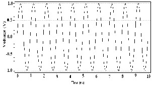
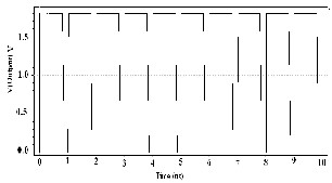
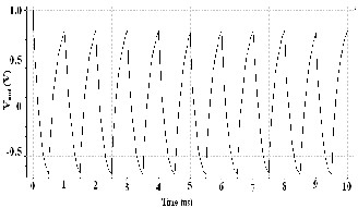
Figure.10.Transient waveforms of Pulse-width Modulator
Moreover, in Fig. 10, we can see the transient
waveform of the Pulse-width modulator and in Fig
11 Shows the average power is of the proposed pulse –width modulator.
TABLE 1
(POWER CONSUMED WITH DIFFERENT VDD )
VDD (Volts) | Power Consumed(watts) |
1.8 | 2.687294e-003 watts |
2.1 | 3.621390e-003 watts |
2.4 | 4.787122e-003 watts |
2.7 | 6.241329e-003 watts |
3.0 | 7.751693e-003 watts |
3.3 | 9.335648e-003 watts |
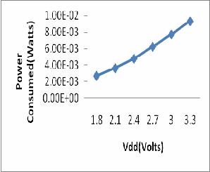
Fig.11 Power consumed with different VDD
Table 1 shows the change in power consumed by the proposed Pulse-width Modulator with different VDD. Fig 11 shows that the power consumed by the PWM circuit in increased linearly with increase in the power supply.
IJSER © 2012
http://www.ijser.org
The research paper published by IJSER journal is about Design and Analysis of Pulse width Modulator (PWM) using Current Comparator 7
ISSN 2229-5518
TABLE2
Power consumed with different Input Voltage
Vin (Volts) | Power Consumed(watts) |
0.1 | 2.659672e-003 |
0.3 | 2.660617e-003 |
0.5 | 2.665467e-003 |
0.7 | 2.674088e-003 |
0.9 | 2.682526e-003 |
1.0 | 2.687294e-003 |
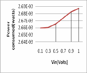
Fig.12. Power consumed with different Input voltage
Table2 is the table of power consumed with different input voltage which is applied at the PWM input. The above graphs shown in Fig.12 is the graph of change in power consumed with different input voltage. This graph shows that the power consumed increase linearly with increase in input voltage.
4 CONCLUSION
In this paper, we have presented a simple Pulse- width Modulator. Pulse width modulation (PWM)
is a powerful technique for controlling analog with
a processors digital outputs.PWM is employed in a wide variety of applications, ranging from measurement and communications to power control and conversion. Experiment results show that the average Power consumed by the proposed Pulse-width modulator is about 9.33mW under the implementation of TSMC 0.35μm CMOS process with 1.8V power supply. The current comparator used in the proposed pulse-width modulator can also compare the voltage input in place of current input. This advantage enables the current comparator to enhance the comparison accuracy while applying to pulse-width modulator. The sample and hold circuit and triangular wave generator, used in the proposed PWM circuit, is designed with an operational amplifier in unity gain configuration. The proposed PWM is simpler than PWM IC form including it can yield the accurate PWM signal with widely operating carrier frequency. In addition the proposed scheme can be also realize in IC form
ACKNOWLEDGMENT
The authors would like to thank Mody Institute of Technology & Science for supporting in carrying out this work.
REFERENCES
[1] Jerald G. Graeme, Application od operational Amplifiers third generation technique. Chapter 5. Mc- Graw hill Book company.1973.
[2] National semiconductor. ‚Op Amp circuit collection.‛
AN-31,1978.
[3] Goldberg J.M. and Sandler, M.B. ‚New high accuracy
Pulse-width modulation based digital to analog converter/Power amplifier.‛ IEEE Proc.- Circuits Device Syst.141,4 (August 1994):315-324.
[4] Mellor, P.H.,Leigh, S.P. and B.M.G. Cheetham,
‚Reduction of Spectral distortion in Class D amplifiersby an enhanced Pulse-width modulation sampling Process.‛ IEEE Prooceeding-G 138,4 (August
1991):441-448.
[5] Bresch , H., Streitenberger, M. and Mathis, W., ‚About the demodulation of PWM-signals with application to audio Amplifiers.‛ Circuits and Systems, 1998. ISCAS
’98.Proceeding of the 1998 IEEE International
symposium. 1(1998):205-208.
IJSER © 2012
http://www.ijser.org
The research paper published by IJSER journal is about Design and Analysis of Pulse width Modulator (PWM) using Current Comparator 8
ISSN 2229-5518
[6] H.Traff, "Novel approach to high speed CMOS current . comparators",Electronics letters,Vol.28, No.3, pp.310-
312, 1992.
[7] A.T.K. Tang and C. Toumazou, "High performance CMOS current comparator",Electronics Letters, Vol.30, No.1, pp.5-6, 1994
[8] B.M. Min and S.W. Kim, "High performance CMOS
current comparator using resistive feedback network", Electronics Letters, Vol.34, No. 22, pp.2074-2076, 1998
[9] Kenneth R. Laker and Will,. M. C. Sansem‛Design of
Analog Integrated Circuits and Systems‛.McGraw Hill.
iiic.. 1994.
[10] Plullip E. Allen and Douglas R. Holberg,‚CMOS Analog Circuits Design‛. Saunders College Publishing,
1987.
Rockey Choudhary is currently pursuing her master’s
degree in VLSI design at Mody Institute of Technology
&Science,Laxmangarh PH- 9414782220
Email: rockeychoudhary @gmail.com
Monika bhardwaj is currently working as faculty in ECE Department at Mody Institute of Technology & Science, Laxmangarh

Email: monika19electrical @gmail.com
Prof. B. P Singh is currently working as Head of ECE Department at Mody Institute of Technology & Science, Laxmangarh.
Email: bpsingh@ieee.org


IJSER © 2012
http://www.ijser.org