International Journal of Scientific & Engineering Research, Volume 5, Issue 5, May-2014 1362
ISSN 2229-5518
Design, Implement and Develop CNT-Metal
Composite PCB Wiring Using a
Metal 3D Printer
Divyashree A.1, Gadhadar C. Reddy2, Shoba B.N.3
Abstract – Carbon Nanotubes are an advanced material that exhibit incredible material properties. They are known to substantially enhance mechanical, electrical and thermal properties of materials with which they are mixed. NoPo has developed techniques for mixing Carbon Nanotubes in Nickel metal matrix. The Nickel-Nanotube composite can be printed in any complex 3D shape using a proprietary CVD technique. The CVD technique is used to print and characterize a CNT-Metal composite conductor for use in Printed Circuit Boards.
Index: Carbon Nanotube, Nickel, Metal Matrix Composite, PCB, W iring
I. INTRODUCTION
CarbonNanotubes are excellent material. They exhibit very high thermal and electrical conductivities[1], [2]. When used as additives with other materials such as metals and polymers; they are known to provide orders of magnitude improvement in material properties of the composite[3], [4].
One such composite was developed at NoPo Nanotechnologies India Private Limited by mixing Single Walled Carbon Nanotubes with a Nickel metal matrix[5]. This technique uses a thermal CVD to produce the metal composite at temperatures of less than 200oC. It can build a layer by layer
3D structure of any thickness.
Three-dimensional printing, technically known as stereo lithographic fabrication, has become increasingly popular, not only among industry but also for personal use. It involves a moving nozzle guided by a computer program laying down successive thin layers of a material, until a three-dimensional object is produced[6], [7].
We have modified this new composite technology to lay out conducting lines on a FR4 PCB board. The CarbonNanotubes provide enhanced conductivity to the 3D printed metal lines. The ease of laying out PCB lines without any need for a mask or screen printing could simplify prototyping PCB’s. A Nickel metal-matrix was chosen as it can be soldered using normal solder lead.
II. RELATED WORK
Chemical vapour deposition (CVD) is widely used in the semiconductor industry for doping silicon. It is also used extensively in the commercial deposition of metals, metal alloys and ceramic coatings[8], [9]. In a typical CVD process, a properly heated substrate is exposed to one or more gaseous chemical precursors, which are then thermally decomposed near the substrate or reduced by an appropriate gas on the
substrate surface to produce the desired deposits. The deposited CVD films usually exhibit good adherence and excellent uniformity in thickness, even on those substrates with irregular shape and sharp corners. With the nature of uniform thickness achieved and bulk deposits capability, 3D components with highly complicated geometry could be fabricated without additional machining or welding.
According to a National Technical Information data search of CVD research report, the applications of the CVD technique ranges from optically and electrically sensitive thin films less than 0.01mm thick to bulk SiC production in the ceramic turbine blade research. Most metals have been deposited by CVD process in the production of thin films[10].
Amongst them, CVD nickel is a promising material owing to its great corrosion resistance . In fact, the low temperature thermal decomposition of nickel tetra-carbonyl (Ni(CO)4) to form nickel deposits with very little contaminations from foreign atoms has been commercially used for many years. Due to the toxic and corrosive features of most reactants, a closed system is usually required when depositing materials with CVD process.
The thermal decomposition of nickel tetra-carbonyl to form nickel deposits involves the reaction
as described in the following:
Ni(CO)4→Ni + 4CO…………………...(i)
Nickel has very good adherence to Carbon Nanotubes. In fact Carbon Nanotubes coated with Nickel are widely used in research. This reaction is widely used in Mond’s process for purification of Nickel from laterite ores[11], [12].
Nickel CVD also known as Nickel Vapor Deposition is widely used in manufacture of master molds for car dashboards. The process is also used to produce ultra high purity nickel. This process was used to build all metal structure for the Sudbury Neutrino Observatory which required Nickel purity of 99.9999% [13].
IJSER © 2014 http://www.ijser.org
International Journal of Scientific & Engineering Research, Volume 5, Issue 5, May-2014 1363
ISSN 2229-5518
A. 3D Printing
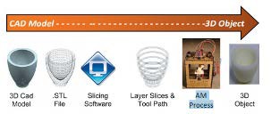
A 3D printer is a computer controlled machine which fabricates the physical objects by depositing materials in successive layers. 3D printing technology enables us to produce physical objects from digital design, created using CAD which is exported to 3D printer.
Figure 1: 3D printing procedure [14]
Unlike traditional machining, 3D printing is an additive process that creates objects by depositing matter one step at a time. Plastic 3D printers are widely available and are used for prototyping and in manufacturing specialized parts. It is superior to traditional machining as it alleviates techniques involving subtractive process. Material wastage is minimal to nil. The only disadvantage of current 3D printing technologies is speed and lack of precision metal 3D printing technologies.
Existing metal 3D printers are modified sintering apparatus[15]. They generally use a laser beam to melt a metal powder and hold it in place. Subsequent layers are deposited and this forms a completed object. The accuracy of a metal 3D printer is ~1mm which is not suitable for a finished product. These machines are also very expensive and use very high temperatures as they have to melt the metal for deposition.
B. Carbon Nanotube Wiring
Carbon Nanotubes exhibit very high conductivity and can withstand very high current densities. These properties could be used to draw conductive lines in electrical circuits. The conductive line can be made extremely thin and still be very conductive. This violates conventional wisdom which states that resistance of a line must increase as we make it thinner according to the formula,
mixed with Carbon Monoxide in order to increase stability and
lifetime of the compound.
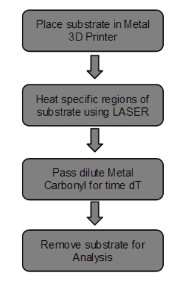
Figure 2: Flowchart of proposed system
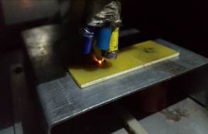
Nickel Carbonyl will deposit on a substrate at a temperature of 120oC. Instead of depositing on a surface and then etching out unwanted regions, we use a high power LASER (HTOE Laser Diode FLMM- 0808) to heat selective regions of the substrate (FR-4 PCB Substrate). The temperature of the select region is monitored remotely using a MLX90614 IR thermocouple. As the LASER pattern is drawn, a Nickel Carbonyl stream is released on the locally heated regions. This causes a uniform deposit of Nickel to be formed.
R = ohmic resistance,
l = length of conductor
A = cross-section area

.............(i)
This aberration is due to the Quantum mechanical behavior of Carbon Nanotubes. They conduct electrons inside their tubular structure instead of on the surface as in a metal[16].
Proposed System:
In the proposed system, Nickel Carbonyl is produced using NoPo Precision Controlled Carbonyl Generator[17]. This system can produce small quantities of Nickel Carbonyl in a concentration that can be specified by the user. The Carbonyl is
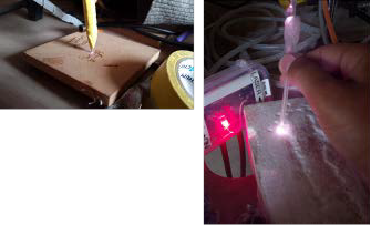
Figure 3: LASER etching of patterns in progress
In order to position the LASER for heating selective regions, we use the 3D printing functionality of the system. A CAD drawing of the PCB circuit is drawn and saved in the
*.STL file format. Any CAD tool including commercial SolidWorks, ProE and AutoCAD can be used for the purpose. The 3D model is then fed into a Slicer program to produce 2D layers from the 3D model. The LASER beam then moves in the pattern of the sliced 2D model.
IJSER © 2014 http://www.ijser.org
International Journal of Scientific & Engineering Research, Volume 5, Issue 5, May-2014 1364
ISSN 2229-5518
For safety reasons, the system is enclosed in a sealed shell.
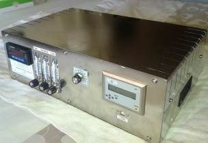
A Chemiluminiscence Nickel Carbonyl Detector is used to monitor Nickel Carbonyl in PPB levels[18]. The detector allows for precise monitoring of Carbonyls inside the printer and for leaks outside.
Figure 6: Nickel CNT deposits
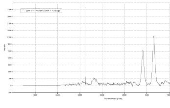
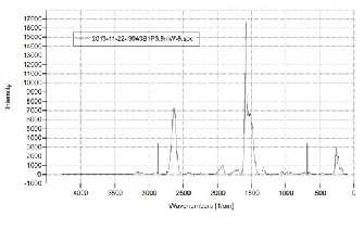
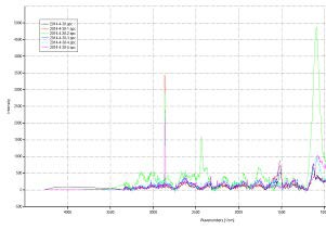
Raman spectra of the nanotubes before being embedded in the metal matrix is as shown below
Figure 4: Nickel Carbonyl Detector
III. RESULT & DISCUSSION
The experiment was performed as described above. During experimentation we found that a solution containing 20-30wt% of SWCNT in alcohol can be directly coated on FR-4 without any need for Nickel metal. The alcohol solution was kept in a ultra-sonicator for 10 mins. This produced a dispersion of nanotubes. This dispersion was then spread out into the required pattern using the 3D printer and simultaneously the LASER beam was turned ON with power rating between
1400W/cm2 to 1600W/cm2 . This instantly vaporized the
alcohol leaving behind a Nanotube layer that seems to adhere well to FR4 substrate. These conducting lines were found to have a resistivity of less than1.2 ohm for line thickness of 1
µm. Comparatively a 1mm wide, 1 micron thick copper wire of length 10mm would have a resistance of 16.8MΩ. (http://www.endmemo.com/physics/resistance.php)
Figure 7: Above: Raman of MWCNT. Below: Raman of
SWCNT
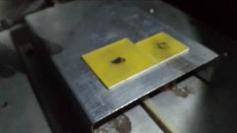
Figure 5: LASER vaporization of CNT-nickel composite
IJSER © 2014 http://www.ijser.org
International Journal of Scientific & Engineering Research, Volume 5, Issue 5, May-2014 1365
ISSN 2229-5518
Figure 8: MWCNT embedded inside Nickel Metal matrix. MWCNT signature lines can be easily seen in the embedded metal matrix.
When the experiment was conducted with Nickel metal deposited from the Carbonyl simultaneously with Carbon Nanotube deposition, it was found that the resulting coating had a high resistance of about 1kΩ. We believe that this might be because of an oxide layer forming on the Nickel metal matrix due to small amount of Oxygen present in the 3D printing chamber. But this resistance is still several orders of magnitude lower than what is present in a thin copper wiring.
IV. CONCLUSION
We have proposed, built and tested a system for printing PCB circuits using a Carbon Nanotube metal matrix composite. We found that Single Walled Carbon Nanotubes sonicated in alcohol and deposited using the high power LASER vaporization process produces excellent conducting lines which is superior to even Nickel –SWCNT lines which we envisioned at the start of the project. .
The system could be used for rapid prototyping of PCB's. It can also be used to manufacture micro-antenna which use a thin di-electric, placed between thin conductive films. The 3D printer offers superior control over deposition and is the only technology capable of forming a metal coating on FR-4 without burning off or damaging the substrate.
REFERENCES
[1] S. Belluci, “Carbon nanotubes: physics and applications,”
Phys. Status Solidi C, vol. 2, no. 1, pp. 34–47, Jan. 2005. [2] S. B. Meo and A. R, “Carbon Nanotubes: Synthesis,
Properties, and Applications,” Crit Rev Solid State Mater
Sci, vol. 26, p. 145, 2001.
[3] A. AGARWAL, S. R. BAKSHI, and D. LAHIRI, “Carbon nanotubes: reinforced metal matrix composites,”
2010.
[4] J. N. Coleman, U. Khan, W. J. Blau, and Y. K. Gun’ko, “Small but strong: a review of the mechanical properties
of carbon nanotube–polymer composites,” Carbon, vol.
44, no. 9, pp. 1624–1652, 2006.
[5] G. Reddy, “A Metal Matrix Based Carbon Nanotube
Composite,” Patent Pending.
[6] “3D Printers Lead Growth of Rapid Prototyping : Plastics Technology.” [Online]. Available: http://www.ptonline.com/articles/3d-printers-lead-
growth-of-rapid-prototyping. [Accessed: 28-Nov-2013]. [7] C. W. Hull, “Apparatus for production of three-
dimensional objects by stereolithography,” US4575330
A11-Mar-1986.
[8] M. J. Hampden-Smith and T. T. Kodas, “Chemical vapor deposition of metals: Part 1. An overview of CVD processes,” Chem. Vap. Depos., vol. 1, no. 1, pp. 8–23, Jul. 1995.
[9] M. J. Hampden-Smith and T. T. Kodas, “Chemical vapor deposition of metals: Part 2. Overview of selective CVD of Metals,” Chem. Vap. Depos., vol. 1, no. 2, pp. 39–48, Sep. 1995.
[10] D. M. Cavagnaro, Chemical Vapor Deposition: Citations
from the NTIS Data Base : Search Period Covered 1975-
1978. NTIS, 1980.
[11] M. Milinkovic, R. P. Reynolds, and D. S. Terekhov, Nickel carbonyl vapour deposition apparatus and method. Google Patents, 2000.
[12] V. Paserin, S. Baksa, A. Zaitsev, J. Shu, F. Shojai, and W. Nowosiadly, “Potential for Mass Production of Nickel-Based Nanomaterials by Carbonyl Process,” J. Nanosci. Nanotechnol., vol. 8, no. 8, pp. 4049–4055,
2008.
[13] J. Boger, R. L. Hahn, J. K. Rowley, A. L. Carter, B.
Hollebone, D. Kessler, I. Blevis, F. Dalnoki-Veress, A. DeKok, and J. Farine, “The Sudbury neutrino observatory,” Nucl. Instrum. Methods Phys. Res. Sect. Accel. Spectrometers Detect. Assoc. Equip., vol. 449, no.
1, pp. 172–207, 2000.
[14] “Could 3D Printing Change the World?,” Atlantic Council. [Online]. Available: http://www.atlanticcouncil.org/publications/reports/could
-3d-printing-change-the-world. [Accessed: 18-Apr-2014]. [15] M. W. Khaing, J. Y. H. Fuh, and L. Lu, “Direct metal
laser sintering for rapid tooling: processing and characterisation of EOS parts,” J. Mater. Process. Technol., vol. 113, no. 1, pp. 269–272, 2001.
[16] A. Bachtold, M. S. Fuhrer, S. Plyasunov, M. Forero, E.
H. Anderson, A. Zettl, and P. L. McEuen, “Scanned Probe Microscopy of Electronic Transport in Carbon Nanotubes,” Phys. Rev. Lett., vol. 84, no. 26, p. 6082, Jun. 2000.
[17] G. Reddy, “A Precision Controlled Carbonyl Generator,” Patent Pending21-Jun-2013.
[18] D. A. Hikade, D. H. Stedman, and J. G. Walega,
“Portable chemiluminescence detector for nickel carbonyl,” Anal Chem, vol. 56, no. 9, pp. 1629–1632,
1984.
IJSER © 2014 http://www.ijser.org
International Journal of Scientific & Engineering Research, Volume 5, Issue 5, May-2014 1366
ISSN 2229-5518

Divyashree A.
The author is currently pursuing M.tech in VLSI and Embedded System at Sapthagiri College of Engineering, Bangalore, Karnataka, affiliated to Visvesvaraya Technological University.
Mr. Gadhadar C. Reddy
Is the Director and CEO at NoPo Nanotechnologies (I) Private
Limited, Bangalore, Karnataka. NoPo is involved in development of advanced technologies based on Single Walled Carbon Nanotubes made in-house using an advanced HiPCO process.
Shoba B N,
Associate Professor in Dept. of Electronic and Communication Engineering, Sapthagiri college of Engineering, Bengaluru, Karnataka .
IJSER © 2014 http://www.ijser.org