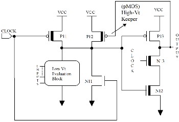
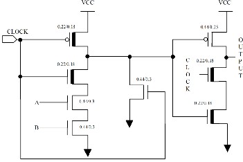
Fig 1(a): Proposed dual-VT domino logic I
International Journal of Scientific & Engineering Research, Volume 3, Issue 6, June-2012 1
ISSN 2229-5518
Design Consideration of Dual Threshold Logic for High Performance and Ultralow Power Carry Look-Ahead Adder
Senthil Sivakumar M, Banupriya M
Abstract— This paper presents the design of high performance and ultralow power 8-bit carry-look-ahead adder circuits using two-phase modified dual-threshold voltage (dual-VT) domino logic method with the feed through logic concept. The proposed concepts are provides lower delay and dynamic power consumption; due to these two advantages it perform better in high fan -out and high switching frequencies. The FTL logic functions can be cascaded in a domino-logic without a need for the intervening inverters. The PMOS high threshold V T keeper increases the circuit speed and reduces the average power consumption. In addition NMOS switch added for avoiding charge sharing problem in pre-charging mode. The additions of two 8-bit binary operands are executed in two cycles. It found that, the circuit is suitable for long adders; the dynamic power consumption is also drastically red uced by more than 50% by the measurement results. This proposed CLA method reducing power (50%) and propagation time delay (around 20%).
Index Terms— Carry look-ahead adder (CLA), CMOS; Domino logic, Dual-threshold voltage (dual-VT), FTL logic, Pipeline, Programmable logic array (PLA).
—————————— ——————————
s the demand for higher performance CMOS VLSI pro- cessors with increased complicating grows, we need to improve the performance, area efficiency, and functional- ity of arithmetic circuits. High speed adders are key ele-
ments in digital circuits, like multipliers, microprocessor unit (MPU), application specific integrated circuit (ASIC) designs, and digital signal processing (DSP) chips. Many efforts have been focused on the improvement of adder designs. Since, the use of carry look-ahead (CLA) principle for high speed arith- metic units are remains dominant. One of the challenges in VLSI processor design today is to structure multilevel CLA circuits, specifially for 8-bit integrated circuits without limiting the functional flexibility.
A low power high performance circuit technique was pro- posed in [1] for reducing power dissipation and diminishing
propagation delay of domio logic circuits. The low power FTL dynamic logic is achieved by feedthrough dynamic CMOS logic structure [2]. Wang, Tsai [3] employed 8-bit CLA using dual-VT domino logic blocks which are arranged in a PLA- like manner and synchronously triggered. It is implemented on silicon to verify the power reduction as well as the preserva- tion of high speed. Huang, li lee [4] proposed an 8-bit pipe- lined CLA using the dual-VT domino logic blocks for low power logics. Dual-VT domino logic circuits proposed for reucing subthreshold leakage current in domino logic circuits is proposed in [5].
Domino logic is widely used in high performance inte- grated circuits. It reduces the device count, silicon area and improves the performance of integrated circuits when com-
pared to the standard fully complementary static CMOS logic circuits. However, the major drawback with the domino dy- namic logic circuit is its excessive power decipation due to the switching activityand the clock load. To deal with the exces- sive power dissipation of the dynamic logic, the current de- sign methodologies are employed with power for performance in the delay critical sections of the circuit. This is achieved through a mix of dynamic and static circuit styles, use of dual supply voltages and dual-VT transistors. Domino and dynamic logic’s are mainly affected by charge sharing and race prob- lems. The proposed circuits are giving solution for these prob- lems and minimizing power wastages. In this paper we pro- pose a design consideration of dual threshold logic for ultra- low power high performance CLA logic structure.
Dual-VT Domino Logic Circuits proposed for reducing sub threshold leakage current and power in domino logic circuits [5]. Low power FTL logic is presented in [1]. By utilizing this logic’s, we proposed our new low power dual high-VT domino logic circuits as shown in Fig 1(a) and (b). The domino logic operation is divided into two phases: precharge phase and evaluation phase. In circuit having NMOS logic network (NMOS block), an NMOS transistor (N11) for resetting the output node to low logic level, together with a pull up PMOS load transistor P11. N11 and P11 are controlled by the clock pulses (Clock). The NMOS keeper is used to operate the circuit with minimum delay.
IJSER © 2012
International Journal of Scientific & Engineering Research, Volume 3, Issue 6, June-2012 2
ISSN 2229-5518
Fig 1(a): Proposed dual-VT domino logic I
1) During the precharge phase when clock=0, P11 is on and N11 is off. Then, node (A) is pre-charges towards VDD. The output is kept into previous stage by the clock controlled N13.
2) During the evaluation phase when clock=1, P11 is off
and N11 is on. If the low-Vt evaluation block is evaluated to be
passing the charge at node A should be ground through the
low-Vt evaluation block and N11. The output then is logic high. If the low-VT evaluation block is evaluated to be stop
there will be no discharging path for node A. A keeper PMOS, P12, is added to keep node A at VDD. Then, the output goes to logic low.
A clock-controlled NMOS transistor, N13 in Fig.1 (a), is in- serted in the discharging path of the output inverter. The op-
eration of the modified dual-VT domino logic circuit is similar to that of the typical dual-VT domino logic circuit apart from the pre-charge phase. During the pre-charge phase, clock= 0, P11 is on, N11 and N13 are both off. Thus, P12 is switched off. The output has neither charging path nor discharging path such that the state will be kept as the previous state. This also results in that the circuit to consume less power.
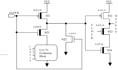
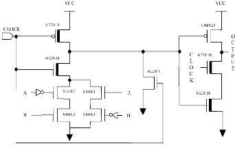
Fig 1(b): Proposed dual-VT domino logic II
The proposed low power circuit is shown in Fig 1(b). It
————————————————
![]() Senthil Sivakumar M is working as a faculty in St.Joseph University, Tanz a- nia. He has received Bachelor of Engineering in Electronics and Communica- tion Engineering from Anna University, India in 2005, and Master of Tech- nology in VLSI Design from VIT University, India. He is published and pre- sented many research papers based on his research projects. Also he was awarded by several integrated circuit companys for his research work.He has a research interest in Low power VLSI Design, Analog and Digital CMOS VLSI Design.
Senthil Sivakumar M is working as a faculty in St.Joseph University, Tanz a- nia. He has received Bachelor of Engineering in Electronics and Communica- tion Engineering from Anna University, India in 2005, and Master of Tech- nology in VLSI Design from VIT University, India. He is published and pre- sented many research papers based on his research projects. Also he was awarded by several integrated circuit companys for his research work.He has a research interest in Low power VLSI Design, Analog and Digital CMOS VLSI Design.
E-Mail: msenthilsivakumar@gmail.com.
![]() Banupriya M is working as a faculty in St.Joseph University, Tanzania. She has received Bachelor of Science from MS Universit, India and Master of Co m- puter Application from Anna University, India. She has a research interest in computer architecture and web designing. She is published and presented some research papers based on her research work.
Banupriya M is working as a faculty in St.Joseph University, Tanzania. She has received Bachelor of Science from MS Universit, India and Master of Co m- puter Application from Anna University, India. She has a research interest in computer architecture and web designing. She is published and presented some research papers based on her research work.
E-mail:mvbanupriya@gmail.com
consists of an NMOS logic network (NMOS block), an NMOS transistor (N21) for resetting the output node to low logic lev- el, together with a pull up PMOS load transistor (P21). N22 and P21 are controlled by the clock signal. N21 is used to con- trol the charge sharing problem; this high Vt NMOS transistor blocks charge sharing while in pre-charging phase.
High VT NMOS switch is driven by clock signal. The pro- posed dynamic logic family is allows to perform the partial evaluation of a computational block before its input signals are valid, and then quickly performs a final evaluation as soon as the inputs arrive. The proposed dynamic logic family is well suited for arithmetic circuits where the critical path is made up of a large cascade of inverting gates.
Consider a long chain of inverters as shown in [1]. When
the clock signal falls, the outputs of the cascaded gates begin to raise the gate threshold voltage to VTH [1]. At this voltage all
the gates in the circuit are in a high gain point. This feature distinguishes the proposed logic family from the other dy- namic logic families. At VTH point any small variation in the input nodes would cause a fast variation of the voltage at the output node. In all other logic families for the output node to begin transition, the inputs need to cross the threshold vol- tage.
Furthermore, when the valid inputs to a gate are asserted,
the gate outputs will only need to make a partial transition from VTH to VOH or VOL through the validation of evaluation
block. The higher performance of the proposed logic circuit is achieved by reducing the propagation delay of both low-to- high and high-to-low transition. However, maintaining the VTH stability for long cascaded circuit structures is a main chal- lenge in this proposed logic, which is the key factor in the fast logic evaluation and high performance of the proposed cir- cuits. In the integrated circuits, VTH stability of cascaded circuit can be achieved by manufacturing technology.
If the propagate signals (Pi) and the generate signals (Gi) of a CLA are produced by combinatorial logic function blocks before they are fed into the function blocks for Si’s and Ci’s, then the Boolean equations of Si’s and Ci’s imply that a two- level AND-OR logic function block is a possible solution to achieve high speed operations. Thus, the PLA styled design is suitable for such a function block. A conceptual PLA styled design for CLA is shown in Fig.3. A typical PLA consists of an AND array and an OR array. It is well known that the series NMOS in the evaluation block of NAND or AND gates will produce long discharging delays which subsequently slow
IJS
http://
International Journal of Scientific & Engineering Research, Volume 3, Issue 6, June-2012 3
ISSN 2229-5518
down the entire circuit.
We can take advantage of the non-inverting feature of the
domino logic to utilize an OR-NOT configuration instead of
the typical AND-OR style, where the two OR planes are made of the modified dual-VT domino logic circuits as shown in Fig
1(b). Mea nwh ile, it can also mi- nim-
ize the series transistor count in the low-VT evaluation block. The OR array is made up of modified dual-VT domino logic with a predefined low-VT evaluation block.
Fig 2: Two stages of proposed dual-VI domino logic I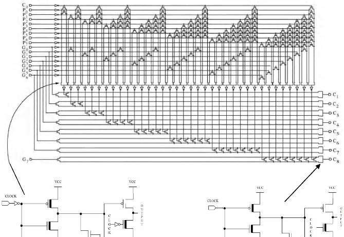
International Journal of Scientific & Engineering Research, Volume 3, Issue 6, June-2012 4
ISSN 2229-5518
Fig 3: PLA – Styled carry lookahead adder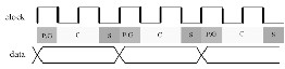
The inputs to the first OR array is the inverted Pi’s and Gi’s signals which are also produced by other modified dual-VT domino logic units as shown in Fig 4. Notably, we define the propagate signals in a different way from the traditional Pi =
Ai + Bi, because the Pi = Ai Bi can be reused to generate the i
sum term, i.e., Si.
The critical path of an adder resides on the generation of carry signals, i.e., C8 in the 8-bit adder. After the binary ope- rands are ready, the generation of Pi’s and Gi’s by using the modified dual-VT domino logic takes the high half of a full cycle. That is, the results of G and P-blocks will be ready when the clock is low.
g 4: (a) G block (b) P block
The inverted Pi’s and Gi’s will then be fed into the first OR plane of the modified dual-VT domino-based PLA. The in- verted outputs of the first OR plane will be presented to the second OR at the high half of the second cycle. The final Ci’s results then are ready in the low half of the second cycle. Right after the generation of every Ci’s, they are inverted and fed into the Si’s function blocks. Another half cycle then is re- quired to produce all of the Si’s. The final result will be latched after two cycles as shown in Fig 5.
Fig 5: Operation timing diagram of the PLA-styled CLA
The transistor count of the PLA-styled implementation for CLA using All-N-Transistor (ANT) logic, an analytic form has been derived in [10]. By the similar derivation method, the number of the total transistors required to implement the pro- posed n-bit CLA with PLA-styled design using the modified dual- VT domino logic is as follows,
(a)
T
Tota l
![]()
![]()
1
(n 1)(n
6![]()
![]()
2)(n 3)![]()
![]()
9
n(n 1)
2![]()
![]()
48n 9
(1)
For instance, for an 8-bit adder using our proposed design, the overall transistor count is 882.
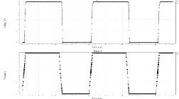
The input and output waveform and comparison chart shown in fig.6. The proposed high performance and low pow- er 8-bit carry-lookahead adder technique increases the circuits speed and reduces the average power consumption. To verify this assertion, simulations were conducted for both circuits of Fig 1(a) and (b). A TSMC 0.18 mm CMOS technology was em- ployed in tanner EDA tool.
IJSER © 2012
International Journal of Scientific & Engineering Research, Volume 3, Issue 6, June-2012 5
ISSN 2229-5518
in the proposed structures. By avoiding these power wastages and dual Vt domino logic technique reduced the total power consumption of circuit. Experiments have shown that high speed and low power obtained by the proposed model match with SPICE simulation results very well. By the experimental verification, the proposed CLA method reduced power more than (60%) and propagation time delay (around 20%).
(a)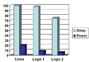
(b)
Fig.6 (a) Output waveform of logic circuit (o/p & i/p),
(b) Comparison chart
The power and delay values are verified using following formulas.Transient power consumption can be calculated us- ing the equation:
The successful completion of any task would be incomplete without the mention of the people who made it possible through their constant guidance and and encouragement crowns all the efforts with success. Most of all, we are very much thankful to Our Parents and Family members whose consistent encouragement, moral support and blessings made to finish this thesis work on time. With great pleasure and pri- vilege I express my sincere thanks to Mr.R.Sakthivel, Asst. Professor (SG), School of Electrical Sciences, VIT Vellore, for his Omni directional guidance throughout the project. We would also like to express our gratitude towards our fellow staff members and students who helped us in every possible way to make this project a success. We express our heartfelt thanks to the VIT University and the Management of the In- stitution for their potential support and provide a good envi- ronment and infrastructure to successful completion of the project.
[1] Saeid Nooshabadi, and Juan A. Montiel-Nelson, ―Fast Feedthrough Logic: A High Performance Logic Family for GaAs‖ IEEE transac- tions on circuits and systems, November 2004.
Where:
Power (PT )
![]()
CPD
![]()
VCC
![]()
![]()
fI NSW
(2)
[2] Victor Navarro-Botello and Juan A. Montiel-Nelson, Saeid Noosha-
badi and Mike DyerLow, ―Power Arithmetic Circuits in Feedth rough
PT Transient power consumption,
VCC Supply voltage,
fI Input signal frequency, NSW Number of bits switching,
CPD Dynamic power-dissipation capacitance.
In the case of single-bit switching, NSW in equation is con-
sidered as 1. Figure of merit of the circuit is measured by,
Dynamic CMOS Logic‖ in 2006 IEEE.
[3] C.-C. Wang, C.-J. Huang, and K.-C. Tsai, ―A 1.0 GHz 0.6- m 8-bit carry lookahead adder using PLA-styled all-N-transistor logic,‖ IEEE Trans. Circuits Syst. II, Analog Digit. Signal Process, Feb. 2000.
[4] Chua-Chin Wang, Chi-Chun Huang, Ching-Li Lee, and Tsai-Wen
Cheng, ―A Low Power High-Speed 8-Bit Pipelining CLA Design Us- ing Dual-Threshold Voltage Domino Logic,‖ IEEE transactions on
Figure of merit
![]()
![]()
Dela y
Power
![]()
Area
(3)
Very Large Scale Integration (VLSI) systems, May 2008.
![]()
The average propagation delay (TPD) is defined as,
[5] J. T. Kao and A. P. Chandrakasan, ―Dual-threshold voltage tech-
TPD
Where,
TPDR
TPDF
2
(4)
niques for low-power digital circuits,‖ IEEE J. Solid-State Circuits, Jul. 2000.
[6] N. Weste, K. Eshraghian, Principles of CMOS VLSI Design, A sys-
tems perspective, Addison Wesley.
TPDR: Rising propagation delay
From input to rising output crossing VDD/2.
TPDF: Falling propagation delay
From input to falling output crossing VDD/2.
In this paper, we have presented an efficient method to minimize power and increase the speed in CLA using dual- Vt and FTL CMOS logic technique. Charge sharing problems as- sociated with dynamic and domino families are also removed
[7] Zhiyu Liu, Volkan Kursun,‖Sleep switch dual thres hold voltage domino logic with reduced subthreshold and gate oxide leakage cur- rent‖ Microelectronics Journal 37 (2006).
[8] Bhaskar Chatterjee, Manoj Sachdev, Ram Krishnamurthy,‖Designing
leakage tolerant, low power wide-OR dominos for sub-130 nm
CMOS technologies―Microelectronics Journal 36 (2005) 801–809.
[9] Seung Hoon Choi, Dinesh Somasekhar, Kaushik Roy, ―Dynamic noise model and its application to high speed circuit design: Micro- electronics Journal 33 (2002) 835–846
[10] C.-C. Wang, C.-F. Wu, and K.-C. Tsai, ―A 1.0 GHz 64-bit high-speed
comparators using ANT dynamic logic with two-phase clocking,‖
IJSER © 2012
International Journal of Scientific & Engineering Research, Vo lume 3, Issue 6, June-2012 6
ISSN 222S-5518
IEEE Proc.Computer Digit. Techn., val. 140, no. 6, pp. 433-436, Nov.
1998.
IJSER lb)2012
htt p://www .'lser. ora