International Journal of Scientific & Engineering Research, Volume 4, Issue 4, April-2013 262
ISSN 2229-5518
DSP based implementation of a Configurable
Composite Digital Transmitter
Soumik Kundu, Amiya Karmakar
Abstract— The latest trend in communications for real time implementation of different transmitters, is a prime contributor to the effo rt being invested in designing and implementing a Composite Transmitter. In this paper, an experimental analysis for the DSP based implementation the composite transmitter, which consists of a combination of four digital modulation schemes, has been presen ted. Extension of the digital domain by implementing and modifying different modulation schemes in software using the same hardware platform of configurable Digital Signal Processor, has been shown.
Index Terms— Binary Modulation, Composite Transmitter, Digital Signal Processing, Modulator, Sampling, Shift Keying Modulation, Signal Processor, Signal-to-Noise Ratio.
—————————— ——————————
1 INTRODUCTION
RANSMITTERS are part of communication systems. De- velopment of a transmitter mainly focuses on developing modulators which are part of the transmitter subsystem.
A modulator is the transmitter subsystem, which is used to facilitate the transmitter for transmitting information in form of signals (digital or analog) [1], [2]. It helps in transmission of signal with lower frequency by shifting the signal’s lower fre- quency spectrum to higher frequency spectrum, using a high frequency carrier signal. In order to develope a modulator the components of a communication system which are required are the information to be transmitted in form of signals (digital or analog), a carrier wave (usually sinusoidal) that carries the information, a channel through which data travels and a modulation scheme that is used by the modulator to modu- lates the incoming data onto the carrier wave with a fixed fre- quency limit imposed by the channel.
With these four components, a transmitter is developed which is Composite and Configurable. This transmitter consists of a composite modulator, which is built with a combination of four digital modulation schemes (BASK, BFSK, BPSK, QPSK). This composition is achieved by union of four modula-
————————————————
Soumik Kundu, School of Engineering & Technology, West Bengal Universi- ty of Technology, India, E-mail: kundu_soumik@yahoo.co.in
Amiya Karmakar, School of Engineering & Technology, West Bengal Uni- versity of Technology, India, E-mail: amiya.karmakar@rediffmail.com
tion schemes [3], [4]. For this reason, this transmitter is named
as Composite. A configurable system is a system whose out- put can be changed without changing its hardware architec- ture using software tools. Digital Signal Processors (DSPs) provide this configurable environment by using a software tool named as Integrated Development Environment (IDE). An IDE provides the basic platform of coding and debugging. In this experiment for implementing the composite transmitter in DSP, the IDE used is Code Composer Studio (CCS). CCS acts as a C compiler that compiles and executes program codes written in C programming languages [5]. It also provides emulation with the Digital Signal Processor. So, composite transmitter C source code is executed in CCS and thereby, output transmitted signals are captured in an oscilloscope.
2 IMPLEMENTATION OF THE COMPOSITE TRANSMITTER
In this section the details of the implementation the composite transmitter system in DSP processor is presented. As men- tioned in the design section, the composite transmitter consists of four digital modulators with the modulation schemes of amplitude shift keying, frequency shift keying, phase shift keying and quadrature phase shift keying respectively. These four modulation schemes are used as algorithms for source codes written in C which are run on the DSK. The arrange- ments of the devices in implementation like connection be- tween the DSK board and PC, connection between DSK and input function generator and output oscilloscope are men- tioned in the following subsection.
IJSER © 2013
http://www.ijser.org
International Journal of Scientific & Engineering Research, Volume 4, Issue 4, April-2013 263
ISSN 2229-5518
We know a transmitter system consists of a input signal to be transmitted, a modulator that will modulate the input sig- nal, a channel through which the modulated signal is trans- mitted, and a carrier that carries the signal. In this experiment, the analog input signal is taken from a function generator, which is a square wave signal with the amplitude 1V (approx.), the modulator is the C source code run on the DSK and the channel used is a wired channel of stereo cables.The modula- tion program is written in C. This program consists of four modules for four digital modulation schemes. It is run on DSK board using the software Code Composer Studio (CCS), as mentioned in the previous chapter. The composite transmitter source code is polling based program. A polling based program is a non interrupt driven program which continuously polls or tests whether or not data are ready to be received or transmit- ted, while the function comm_poll() calls the appropriate func- tions to initialize the DSK [5].The functions input_sample() and output_sample() are used to input and output data respectively. We know, an input signal to the DSK is analog. TLV320AIC23 (AIC23) Onboard Stereo CODEC converts this analog signal into digital signal using the process of sampling and quantiza- tion [5]. The input_sample() function returns samples of the input signal. This samples are compared with a threshold val- ue 0, in order to generate the binary bit stream of 0s and
1s.Though the transmitter is composite, we cannot transmit all
four modulated signal all together. But here a special mecha- nism is used to transmit a particular modulated signal at a time. This special mechanism is the use of the DSK DIP switches and LEDs [5]. As mentioned in the earlier chapter, there four DIP switches, these four DIP switches are used for transmission of four modulated signal, i.e., switch 0 for BASK signal, switch 1 for BFSK signal, switch 2 for BPSK signal and switch 3 for QPSK signal, as shown.
From the basic concepts of modulation, we know that a carrier signal is required to transmit the input signal. In this transmitter system, a sinusoidal carrier of frequency 8000 Hz and 1.6V (approx.) amplitude has been used for this purpose. In the program, sine tables are used for this carrier. These sine tables are generated as header file from a MATLAB M file [5]. The connectivity between the DSK and PC and between the DSK and function generator and oscilloscope is made for emulation and capturing output signals in oscilloscope. The DSK board TMS320C6713 consists of two input channels LINE IN and MIC IN and two output channels LINE OUT and MIC OUT. The input channel LINE IN is connected to a function generator and output channel LINE OUT is connected to an
oscilloscope. Some snapshots of the transmitted signals have been presented in the following Fig. 1.
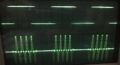

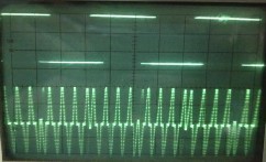
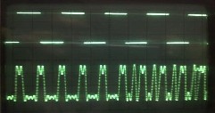
Fig 1. Snapshots of the four transmitted signals taken from oscillo- scope
3 Development of a Composite Modulation
Algorithm
The composite modulation algorithm is developed with the combination of four digital modulation schemes of BASK, BFSK, BPSK and QPSK respectively. The following flowcharts describes the composite modulation scheme along with indi-
vidual modulation schemes of BASK and QPSK. The flowchart
IJSER © 2013
http://www.ijser.org
International Journal of Scientific & Engineering Research, Volume 4, Issue 4, April-2013 264
ISSN 2229-5518
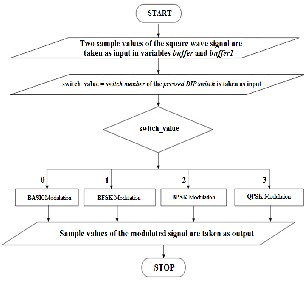
of the Fig. 2 shows how the composite modulation program works. The program takes two inputs, one is sample values of the input square wave signal taken in variables buffer and buff- er1, and another is the switch number of the pressed DIP switch. According to the switch number, one of the four modulation program module is selected. The selected program module gen- erates the sample values of the modulated signal, which is tak- en as output.
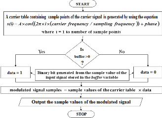
Fig 3. Flowchart of the BASK Modulation Scheme
Fig 2. Flowchart of the Composite Modulation Scheme
The following Fig. 3 is the flowchart of BASK modulation program module used in the composite modulation program. A carrier table containing 32 sample points of the cosine carrier signal is generated by using the equation (given in the flowchart) at phase = 0. As mentioned earlier, the binary bits are generated from the sample values of the input square wave signal. These binary bits are multiplied with the sample points of the carrier table to generate the sample value of the BASK modulated signal.
The flowchart of the QPSK modulation program module of the composite modulation program is present in the following Fig. 4. In the composite modulation program flowchart, it have been shown that two sample values of the input square wave signal are taken as input to variables buffer and buffer1 respec- tively. The values of these two variables are used to generate an even and odd bit respectively, using the same logic for gener- ating the binary bit mentioned in flowchart of BASK modula- tion program module (Fig. 3). These two bits are converted into bipolar bits of -1 or 1 and stored in the variables bipolar even bit and bipolar odd bit respectively. Then, the even bipolar bit is multiplied with the sample points of the cosine carrier table and odd bipolar bit is multiplied with the sample points of the sine carrier table. The two products obtained from the previous calculation, are added to get the sample value of the QPSK modulated signal.
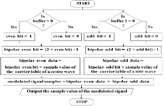
Fig 4. Flowchart of the QPSK Modulation Scheme
IJSER © 2013
http://www.ijser.org
International Journal of Scientific & Engineering Research, Volume 4, Issue 4, April-2013 265
ISSN 2229-5518
4 Performance Analysis with Signal to Noise
Ratio
Signal-to-noise ratio (often abbreviated SNR or S/N) is a meas- ure used in science and engineering that compares the level of a desired signal to the level of background noise. It is defined as the ratio of signal power to the noise power. Noise levels in a digital system are expressed using SNR, which is the ratio of Eb/Pn, the energy per bit per average noise power spectral density. MATLAB has been used as a tool for determining the SNR and plotting of Eb/Pn graph.
4.1 Signal Power and Energy
Suppose we have a signal x(n), where n is an index of the sample number. We define the instantaneous power of the signal as,
contain the modulated signal sample values at three different input signal frequency and carrier frequency of 8 KHz. From these samples 50 samples are taken for the calculation of Eb.
4.2 Noise
In this calculation of signal to noise ratio, the transmitted sig- nal is assumed to be perturbed by an additive, zero-mean, sta- tionary, white, Gaussian noise, denoted by W(t). The reasons for this assumption are that it makes calculation traceable, and also it is reasonable description of the type of front end receiv- er noise present in many communication systems. Another assumption is made in this context that is the transmission channel is linear, with a bandwidth that is large enough to accommodate the transmission of the modulated signal.The average noise power Pn is generally expressed as noise power
spectral density of N0/2, where the constant N0 = kt × fs
Pins x2 (n)
(1)
(Boltzmann constant × room temperature in Kelvin × Sam- pling Frequency), whose value is 6.4 × 10⁻¹⁷ W/s, taking k=
In other words, the instantaneous power of a sample is just the value of that sample squared. Since the units of the sample are volts, the units of the power are watts. A far more useful quan- tity is the average power, which is simply the average of the instantaneous power of every sample in the signal. For signal x(n), of N samples, we have:
1.38 × 10⁻²³ J/0K , t = 2900 K and fs = 32000 Hz.
4.3 Results for performance analysis with signal to noise ratio
By considering the assumptions specified in the previous sub- section, the values of SNR for each of the four modulated sig-
nals transmitted by the composite transmitter are as follows:
Pave
N

x2 (n) (2)
N n1
By definition, power is the time derivative of energy; or equivalently, energy is the time integral of power. For sam- pled signals, integration reduces to a summation. Since energy is the product of power and time, the total energy of a signal must be equal to its average power multiplied by its duration. Furthermore, the duration of a signal is its length in samples, divided by the sampling frequency, in samples per second.
Therefore:
Eb Pave.t
(3)
N


x2 (n). (4)
N n1 fs
N

x2 (n) (5)
fs n1
In the DSP implementation of the composite transmitter the sampling rate used is 32 KHz. Twelve files are generated from the execution of the composite transmitter code. These files
Table 1. Table for result of performance analysis with SNR
SNR values obtained are significantly greater than zero, which reveals the fact that the effect of white noise on the modulated signal during transmission is almost negligible. The average SNR value for four modulation schemes is 228 dB, which is the maximum acceptable SNR value for a modulated signal transmission in the presence of white noise. Moreover, the
SNR value less than zero reveals the fact the noise power is
IJSER © 2013
http://www.ijser.org
International Journal of Scientific & Engineering Research, Volume 4, Issue 4, April-2013 266
ISSN 2229-5518
greater than the signal power, which is not accepted for signal transmission. So, in this case the acceptable range of signal to noise ratio is from 0 to 228 dB. From these results, a graph be- tween Eb and Pn is plotted, as shown in the following diagram.
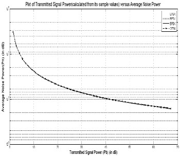
Fig 5. Graph of Transmitted Signal Energy versus Average Noise
Power
4 CONCLUSION
The idea of composition is utilized in the DSP based imple- mentation of a composite transmitter. For this implementa- tion, a single program containing four digital modulation schemes is executed in the DSK board; from which four modu- lated signals are generated. It is a very simple implementation compared to conventional methodology in which the transmit- ters are developed with analog circuitry. It is also a very cost effective as we have implemented four modulation schemes together into a single modulator on the same hardware plat- form using the switching facility of the DSK board and a soft- ware support tool.
REFERENCES
[1] J. D. Oetting, A Comparison of Modulation Techniques for Digital
Radio, IEEE Transactions on Communication, Vol. COM-27, No. 2, pp.
1752-1762, December 1979.
[2] T. D. Memon, W. Ghangro, Dr. B. S. Chowdhry, A. A. Shaikh, Quad- rature Phase Shift Keying Modulator & Demodulator for Wireless Modem, 2nd IEEE Conf. on Computer, Control and Communication, Ka-
rachi, pp. 1-6, 2009.
[3] J.C. Pliatsikas, C. S. Koukourlis and J. N. Sahalos, On the Combining of the Amplitude and Phase Modulation in the Same Signal, IEEE Transactions on Broadcasting, Vol. 51, No. 2, pp. 230-236, June 2005.
[4] A. Karamakar, A. Sinha, A novel architecture of a reconfigurable radio processor for implementing different modulation schemes, 3rd IEEE Conf. on Computer Research and Developement (ICCRD), Shanghai, vol. 1, pp. 115-119, 2011.
[5] Rulph Chassaing, Digital Signal processing and Applications with the
C6713 AND C6416 DSK, Hoboken, NJ: John Wiley and Sons, 2005.
IJSER © 2013
http://www.ijser.org