
1
International Journal of Scientific & Engineering Research Volume 2, Issue 11, November-2011
ISSN 2229-5518
“Design of High Gain Folded-Cascode Operational Amplifier Using 1.25 um CMOS Technology”
Er. Rajni
Abstract This paper presents a design of the Folded-cascode operational amplifier using 1.25µm CMOS technology, which leads to high gain as compared to a normal cascode circuit. The simulation of the cascode and folded cascode circuits is done using TSPICE simulation tool and the LEVEL–2, 1.25 µm parameters are used. A complete analysis of the circuit is presented in this paper which shows how this circuit leads to a high gain and resistance at output. A comparison between the cascode and Folded-Cascode op amps is described. We have also described their simulated and calculated results comparison individually. This paper provides a considerable insight into the overall operation and advantages of the folded-cascode circuit. This design overcomes some limitations and drawbacks of the various previously presented described architectures.
Index Terms Operational amplifier, complementary metal-oxide semiconductor, common-mode range, input common-mode range, power-supply rejection ratio.
—————————— ——————————
digital (A/D) and digital-to-analog (D/A) converters, input
he design of op amps continues to pose a challenge as the supply voltage and transistor channel length scale down with each generation of CMOS technologies. Operational amplifiers are the amplifier (controlled sources) that has sufficiently high gain so that when negative feedback is applied, the closed loop transfer function is practically independent of the gain of the op amp. This principle has been exploited to develop many useful analog circuits and systems. The primary requirement of an op amp is to have an open-loop gain that is sufficiently large to
implement the negative feedback concept.
Different architectures have been used [10],[11],[12],[13] to
obtain high gain bandwidth, output resistance and power-
supply rejection. Two-stage Cascode op amps circuits are widely used in circuit designs at places where high gain and high output impedances are required. Folded cascade gives better performance even than the cascode op amp circuit.
These architectures have been compared, using TSPICE
and output signal buffers, and many more, and to compare its
some of the performance parameters with the two-stage
cascode op-amp by designing cascode op-amp for the almost same specifications.
The paper is organized as follows: in section-2 we present all the configurations for simulating and measuring the above specified and many other characteristics. The section-3 gives conclusion of this paper.
As we know the input signal of a common-gate stage may be a current and also that in the common-source arrangement a transistor converts a voltage signal to a current signal. The cascade of a CS stage and a CG stage is called a ‘cascode’ topology, which provides many useful properties. Fig.2.1 shows the basic configuration: M1 generates a small signal drain current that is proportional to
simulations, in this paper along with drawbacks and
Vin
and M2 simply routes the current to RD . We call M1 the
advantages of each.
The difference between an Operational Transconductance Amplifier (OTA) and an Operational Amplifier (Op-Amp) is that the op-amp has got an output buffer so that it is able to drive resistive loads. An OTA can only drive capacitive loads.
Our goal is the design analysis and simulation of a High Gain Folded-Cascode Op Amp using CMOS process in order to use it in wide applications ([7],[14],[17],18]) like in the design of high-order filters, signal amplifiers, analog-to-
input device and M2 the cascode device. Note that in this
example, M1 and M2 carry equal currents. As we describe
the attributes of the circuit in this section, many advantages
of the cascode topology over a simple Common-Source stage become evident. [Razavi, design of Analog CMOS Integrated Circuits]
————————————————
Author is currently working as Assistant Professor at JCDM college of
Engg., Sirsa(Hry), India. E-mail: er.rajni08@gmail.com
IJSER © 2011
2
International Journal of Scientific & Engineering Research Volume 2, Issue 11, November-2011
ISSN 2229-5518
Figure.3.1 Two-stage Cascode op amp
Figure.2.1 Cascode stage
1. VDD
VSS =2.5V
2. Slew rate = 5V/ s with a 50 pF load
3. GB = 10MHZ with a 10 pF load
4. Av 5000V/V
5. ICMR = -1 to +1.5V
6. Output swing = 1.5 V
1. Slew rate =
I out
![]()
C L
(1)
g m1 g m6 g m8
![]()
2. (2)
2g m3CL
g m1 g m6 g m8
Figure.2.2 Input-output characteristics of a cascode stage
3. Av
![]()
![]()
g m3 2
RII
(3)
4. Positive CMR
I 5
![]()
Vin (max) VDD
| VTO3 | (max) VT 1 (min)
3
(4)
5. Negative CMR
Vin min VSS VDS
sat
I 5
1 / 2
VT 1 (max)
(5)
![]()
5
1
IJSER © 2011
3
International Journal of Scientific & Engineering Research Volume 2, Issue 11, November-2011
ISSN 2229-5518
![]()
6. g m
2 K N ,P S N , P I D
(6)
7. g ds I D
8. rds 1/ I D

(7)
(8)
9. VDS
(sat)
2I DS
(9)
![]()
10. The overall gain of the input stage is
AvI
g m2 / g m4 g m1 / g m3
(10)
11. The gain of second stage is
g m6 g m8
AvII
![]()
RII
2
(11)
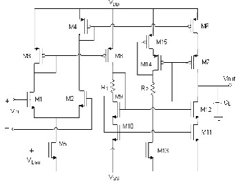
Figure 4.1 Proposed folded cascode op amp
Where RII
is given by
1. Power Supply, VDD
VSS 2.5V
![]()
RII
g m7 rds7 rds6 g m12rds12rds11
(12)
2. Slew rate (SR) = 10V/ S
3. Load capacitance, C L = 10pF
therefore
Av g m1 / 2g m4 g m6 g m8 kRII
(13)
4. Output Voltage Swing ( Vout (swing)) = 2V
5. Gain Bandwidth (GB) = 10MHz
TABLE 4.1. TRANSISTOR SIZING OF THE TWO-STAGE CASCODE OP AMP CIRCUIT OF FIG.4.3
1 2 1 2
6. Input Common-Mode Voltage Range (ICMR) = -
1.5V to +2.5V
7. Differential Voltage Gain ( v ) 5000V/V
8. Power Dissipation 5mW
I 3
![]()
5 5 1. Slew rate =
C L
S13
14 15
13
14 15
2. Bias currents in output cascodes, avoiding zero currents in cascodes
I 4 I 5 1.2I 3to1.5I 3
3. Using maximum output voltage, vout max
![]()
S 2I 5 , S
![]()
2I 7
(14)
5 ' 2 7 ' 2
K PVSD5
K PVSD7
IJSER © 2011
4
International Journal of Scientific & Engineering Research Volume 2, Issue 11, November-2011
ISSN 2229-5518
VSD5
sat V
SD7
![]()
sat VDD Vout min
2
(15)
10. Power dissipation
Pdiss VDD VSS I 3 I12 I10 I11
(25)
LetS 4 S14 S5 and S13 S6 S7
(16)
11.Positive CMR
I 5
Vin (max) VDD
| VTO3 | (max) VT 1 (min)
![]()
4. Using minimum output voltage, Vout min
3
VDS 9
sat V
DS11
![]()
sat Vout min | VSS |
2
(17)
12. Negative CMR
Vin min VSS VDS
sat
I 5
1 / 2
VT 1 (max)
5
S11
![]()
![]()
2I11
' 2
S9
![]()
2I 9
(18)
1
K NV
DS11
K ' N V 2 DS 9
13. R9 g m9 rds9 rds11
(26)
Let S10 S11 and
5. Self-bias cascade
S8 S9
(19)
14. The second stage resistance is
RII
R9
![]()
![]()
1
![]()
g m7 g g g
(27)
R1 VSD14 sat \ I14 and
R2 VDS 8 sat \ I 6
(20)
ds7
ds2
ds5
![]()
6. GB g ml
CL
RII
![]()
g m9 rds9 rds11 g m7
g
![]()
1
ds7
![]()
ds2
g ds5
g 2 ml
![]()
GB2 C 2 L
(28)
![]()
S1 S 2 '
K N I 3
K ' N I
(21)
15. The small-signal voltage gain is given by
7. Using minimum input CM
2 k
![]()
(29)
S3
2I 3
![]()
'
Vin
min VSS
![]()
2
I 3
' VT 1
v g mI RII
2 2k
K N
K N S1
R g
g
9 ds2 ds4
8. Using maximum input CM
(22)
where k
'
g m7
rds7
S 4 and S 5 must meet or exceed the requirement of step
3
16.
![]()
g m
2 K N ,P S N , P I D
S 4 S5
![]()
2I 4
K P VDD Vin max VT 1
(23)
17.
18.
g ds I D
rds 1/ I D
9. Differential voltage gain
![]()
vout g m1
g m 2 R
2 k g R 2I
![]()
![]()
v 2
![]()
21 k II
![]()
m1 II
2 2k
19. V
(sat) DS
in
(24)
DS
IJSER © 2011
5
International Journal of Scientific & Engineering Research Volume 2, Issue 11, November-2011
ISSN 2229-5518
TABLE 4.2.1 TRANSISTOR SIZING OF THE PROPOSED FOLDED CASCODE OP AMP CIRCUIT OF FIG. 4.1
The following table shows the comparison between the performance parameters taken in specifications for the design and that resulted after simulations of the Folded Cascode Op Amp.
TABLE.5.4. RESULTS FOR THE FOLDED CASCODE OP-AMP
For simulating the proposed cascode and the folded cascode
Op-Amp topologies in TSPICE, 1.25m CMOS technology
parameters [TSPICE model ml2_125] taken for NMOS and PMOS transistors are as mentioned in Table.5.1 and Table.5.2.
TABLE.5.1 PARAMETERS OF NMOS
circuits, having the loading capacitance of
10 pF , dual
voltage supply of
2.5V
and using the CMOS 1.25m
TABLE.5.2 PARAMETERS OF PMOS
technology. For comparison, the transistors used in op amps have been sized for almost same specifications.
Simulated results show that this op amp exhibits high DC
gain, improved ICMR. The typical values for DC gain is of the order of 6.035KV / V , ICMR is of the order of -1.0V to
2.5Vand unity gain bandwidth of the order of 8MHz have been obtained.
IJSER © 2011
International Journal of Scientific & Engineering Research Volume 2, Issue 11, November-2011
ISSN 2229-5518

6
(3)

(1)
2. AC RESPONSE MEASUREMENT:
4. PSRR MEASUREMENT:
A small sinusoidal voltage is inserted in series with
VDD (VSS )
to measure PSRR+ (PSRR-). Here we are
(2)
The slew rate is calculated by changing the inputs of the op amp to pulsed, and measuring the slope at the differential output of the op amp. The slope of the output at the rising edge gives the positive slew rate of the amplifier, and the slope of the output at the falling edge gives the negative slew rate of the amplifier. The positive slew rate of the
inserting a small ac voltage of 1V. We get PSRR of 55dB.
(4)
Figure 5.1 Simulated Waveforms of Folded Cascode Op Amp
designed amplifier is 8.55 rate is 6.72 V / s
.
V / s
and the negative slew
IJSER © 2011
7
International Journal of Scientific & Engineering Research Volume 2, Issue 11, November-2011
ISSN 2229-5518

TABLE 5.5. RESULTS FOR THE TWO STAGE CASCODE OP-AMP
(2)

3. TRANSIENT RESPONSE MEASUREMENT:
1. INPUT COMMON MODE RANGE MEASUREMENT:


4. PSRR MEASUREMENT:
(3)
(1)
2. AC RESPONSE MEASUREMENT:
(4)
Figure 5.1 Simulated Waveforms of Cascode Op Amp
IJSER © 2011
8
International Journal of Scientific & Engineering Research Volume 2, Issue 11, November-2011
ISSN 2229-5518
The comparison of the design and simulations of the two- stage cascode and the folded cascode op amps can be sum up in the table below.
TABLE 5.3. COMPARISON RESULTS BETWEEN CASCODE AND FOLDED CASCODE OP-AMPS
S.No. | Parameter | Two-stage cascode op- amp | Folded cascode op-amp |
1. | Voltage Gain | Low (4721 V/V) | High (6053V/V) |
2. | ICMR | Low (-0.0 to 0.5V) | Very High (- 1.0V to 2.5V) |
3. | PSRR | Very Low (25dB) | High (60dB) |
4. | Output Resistance | Low (8.5 M ) | High (130 M ) |
This paper presents design analysis of the Folded-cascode amplifier using 1.25 µm CMOS technology. Initially our work describes the design of two-stage cascode op amp using the same i.e. 1.25 µm technology and then to overcome some of the limitations of the cascode op amp we have designed a high gain folded-cascode op amp which provides a high output resistance which leads to high gain as compared to a normal cascode circuit. The simulation of the cascode and folded cascode circuits is done using TSPICE simulation tool and the LEVEL–2, 1.25 µm parameters are used. A complete analysis of the circuit is presented in this thesis which shows how this circuit leads to a high gain and high resistance at output. A comparison between the cascode and Folded-Cascode op amps is described. We have also described their simulated and calculated results comparison individually. This paper provides a considerable insight into the overall operation and advantages of the folded-cascode circuit. This design overcomes various limitations and drawbacks of the various previously presented described architectures.
In this paper, a folded cascode op amp has been designed in
1.25m CMOS technology. This op amp structure is used
for many applications. Simulated results show that this op
amp exhibits high DC gain, improved PSRR and ICMR and
large output voltage swing. The typical values for DC gain is of the order of 6.035KV / V , ICMR is of the order of -1.0V to 2.5V, PSRR is 55dB , output swing is of the order of -
2.3V to +2.0V, unity gain bandwidth of the order of 8MHz
PMOS for proper operation and also finding different gains, currents in all the branches, resistances shown in circuits. But after careful analysis of simulation and designing at different points, the goal was achieved. The op amp fulfills all the other requirements with a good margin and has been simulated for worst cases.
Therefore the proposed folded cascode op amp exhibits the following advantages over the two-stage cascode op amps:
Improved DC gain
Improved ICMR
Better PSRR
[1] M. Banu, J. M. Khoury, and Y. Tsividis, ―Fully Differential Operational amplifier with Accurate Output Balancing,‖ IEEE Journal of Solid State circuits, Vol. 23, No. 6, pp. December
1990.
[2] B. G. Song, 0. J. Kwon, I. K.Chang, H. J. SONG and K. D.
Kwack,‖A 1.8V Self-Biased Complementary Folded-Cascode
Amplifier‖, IEEE J. Solid State circuits pg. No. 63-65, 1999.
[3] Bazes, "Two novel fully complementary self- biased CMOS differential amplifiers", IEEE J. of Solid-state Circuits, vol 26, No 2, pp. 165-168, Feb. 1990.
[4] E. Sacking and W. Guggenbuhi, "High-swing, high- impedance MOS cascode circuit", IEEE J. of Solid-state Circuits, vol 25, No 1, pp. 289-298, Feb. 1991.
[5] R. E. Vallee and E. I. El-Masry, "A very high-frequency CMOS complementary folded cascode amplifier," IEEE J. of Solid- state Circuits, vo1.29, no. 2, pp. 130-133, Feb. 1994.
[6] Pradeep Mandal and V. Visvanathan, "A self-biased high performance folded cascode Op-Amp", IEEE 10th International Conference on VLSI Design, pp.429-434, Jan.,
1997.
[7] Olivera-Romero and Silva-Martinez, ―A folded-cascode OTA based on complementary differential pairs for HF applications,‖ Design of Mixed-Mode Integrated Circuits Design and Applications, pp. 57–60, Jul. 1999.
[8] Roewer and Kleine, ―A novel class of complementary folded cascode opamps for low-voltage,‖ IEEE J. Solid- State Circuits, vol. 37, no. 8, pp. 1080–1086, Aug. 2002.
[9] Yan and Allstot, ―Considerations for fast settling operational
amplifiers,‖ IEEE Trans. Circuits Syst., vol. 37, no. 3, pp.
326–334, Mar. 1990.
[10] Milton Wilcox, "High Frequency CMOS switched capacitor filters for communications applications ", IEEE Journal of Solid State Circuits, vol. SC-18, No. 6, December 1983.
[11] P. Naus et al. , "A CMOS stereo 16-bit convertor for digital
and slew-rate of
8.55V / s
have been obtained. Most
audio", IEEE J. Solid State Circuits, vol. SC-22, no. 3, 1987, pp.
390-395.
difficult part in this design was optimization of NMOS and
IJSER © 2011
[12] S.H. Lewis and P.R. Gray, "A pipelined 5-Msamples 9-bit
9
International Journal of Scientific & Engineering Research Volume 2, Issue 11, November-2011
ISSN 2229-5518
analogto-digital conVertor", IEEE J. Solid State Circuits, vol. SC-22, no. 6, 1987, pp. 954-961.
[13] S. Wong and C.A.T. Salama, "Impact of scaling on MOS analog performance", IEEE J. Solid State Circuits, vol. SC-18, no. 1, 1983, pp.106-114.
[14] R.G. Eschuzier, L.P.T. Kerklaan, and J.H.Huising, ―A 100
MHz 100dB Operational Amplifier with Multipath Nested Miller Compensation, ―IEEE J. of Solid State Circuits, vol.27,pp.1709-1717, Dec. 1992.
[15] Ziazadeh, H.T. Ng, and D.J.Allstot, ―A Multistage Amplifier
Topology with Embedded Tracking Compensation, ―CICC
proc.,pp.361-364,May 1998.
[16] M. Loulou, S. Ait Ali, M. Fakhfakh, and N. Masmoudi Laboratoire d’Electronique et des Technologies de l’Information, LETI. National Engineering School of Sfax Tunisia..,‖ An Optimized Methodology to Design CMOS
Operational Amplifier‖ IEEE J. Solid State Circuits, 2002, pp.
no. 14-17.
[17] Analog IC Design Project ―Folded Cascode Operational
Amplifier‖ submitted by Rahul Prakash 12/06/04.
[18] B. G. Song, 0. J. Kwon, I. Caching, H. J. SONG and K. D.
Kwack,‖A 1.8V Self-Biased Complimentary Folded Cascode
Amplifier‖, IEEE, AP-ASIC ’99,pp-63-65, 1999.
[19] http://metalab.uniten.edu.my/~./microe/files/OPAMP_
[20] M. Loulou, S. Ait Ali, M. Fakhfakh, and N. Masmoudi ―An Optimized methodology to Design CMOS Operational Amplifier‖, IEEE journal ,pg. No. 14-17,2002
[21] CMOS Operational Amplifier‖, IEEE journal ,pg. No. 14-
17,2002
IJSER © 2011