International Journal of Scientific & Engineering Research Volume 2, Issue 9, September-2011 1
ISSN 2229-5518
Comparison of CMOS and Adiabatic Full Adder
Circuits
Y.Sunil Gavaskar Reddy, V.V.G.S.Rajendra Prasad
Abstract— Full adders are important components in applications such as digital signal processors (DSP) architectures and microprocessors. Apart from the basic addition adders also used in performing useful operations such as subtraction, multiplication, division, address calculation, etc. In most of these systems the adder lies in the critical path that determines the overall performance of the system. In this paper conventional complementary metal oxide semiconductor (CMOS) and adiabatic adder circuits are analyzed in terms of power and transistor count in 0.18um technology.
Index Terms— Low-power, adiabatic logic, Full adder, CMOS, Pass transistor logic, Positive feed back adiabatic logic, Transmission gate logic
—————————— ——————————
ower minimization is one of the primary concerns in today VLSI design methodologies because of two main reasons one is the long battery operating life requirement of mobile
and portable devices and second is due to increasing number of transistors on a single chip leads to high power dissipation and it can lead to reliability and IC packaging problems.
Power dissipation can be reduced by employing different techniques at different levels of abstraction of the IC design process (system, algorithmic, architecture et al.). At the circuit level, power dissipation in CMOS Logic is related to kCV2 where k is switching activity, C is load capacitance and V represents supply voltage. General approaches for reducing power consumption at circuit level are reducing the power supply voltage, reducing switching activity or reducing load capacitance [1],[2]. Another approach for reducing power dis- sipation at the circuit level is usage of AC power supply for recycling energy of node capacitances. The principle is known as adiabatic which is taken from thermodynamics. In literature, there are two kinds of adiabatic circuits presented one is full- adiabatic and other is quasi-adiabatic or partial adiabatic cir-
details of conventional charging and adiabatic charging prin- ciple, Section 3 explains different full adder implementations, section 4 simulation results and finally sec 5 is conclusion.
The operation of adiabatic logic gate is divided into two dis- tinct stages: one stage is used for logic evaluation; the other stage is used to reset the gate output logic value. Both the stag- es utilize adiabatic switching principle. In the following section conventional switching and adiabatic switching analyzed in detail.
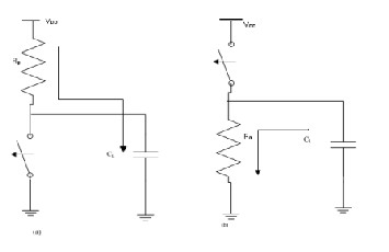
There are three major sources of power dissipation in digital CMOS circuits those are dynamic, short circuit and leakage power dissipation. The dominant component is dynamic pow- er dissipation and is due to charging, discharging of load capa- citance [2]. The equivalent circuits of CMOS logic for charging and discharging is shown in Fig.1. The expression for total power dissipation is given by.
cuits. [1]
Addition is one of the important and commonly used
arithmetic operation in many signal processing and other ap- plications. So, an adder is one of the most critical components
of a processor which determines its throughput, as it is used in the ALU, the floating-point unit, and for address generation in case of cache or memory access. In this paper we present dif- ferent full adder designs based on adiabatic and conventional CMOS logic principle and their performance based on the power dissipation compared.
The rest of the paper is organized as follows. Section 2 gives
Ptot .CL .V .VDD . fclk I SC .VDD Ile .VDD
(1)
————————————————
Fig.1. Conventional CMOS a) Charging b) Discharging
IJSER © 2011
International Journal of Scientific & Engineering Research Volume 2, Issue 9, September-2011 2
ISSN 2229-5518
Equation (1), the first term represents the dynamic power, where CL is the loading capacitance, fclk is the clock frequen- cy, and α is the switching activity. In most cases, the voltage swing V is the same as the supply voltage Vdd; however, in some logic circuits, the voltage swing on some internal nodes may be slightly less. The second term is due to the direct-path short circuit current Isc which arises when both the NMOS and PMOS transistors are simultaneously active, conducting cur- rent directly from supply to ground. Finally, leakage current Ile which can arise from substrate injection and sub threshold ef- fects is primarily determined by fabrication technology consid- erations. [2], [4]
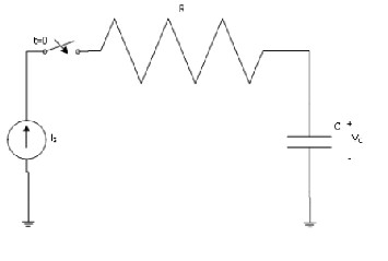
Adiabatic switching can be achieved by ensuring that the po- tential across the switching devices is kept arbitrarily small. This can be achieved by charging the capacitor from a time- varying voltage source or constant current source [1], [4], [9], as shown in Fig. 2. Here, R represents the on-resistance of the pMOS network. Also note that a constant charging current cor- responds to a linear voltage ramp.
be made small by increasing the charging time. A portion of the energy thus stored in the capacitance can also be reclaimed by reversing the current source direction, allowing the charge to be transferred from the capacitance back into the supply. Adiabatic logic circuits thus require non-standard power sup- plies with time-varying voltage, also called pulsed power sup- plies. The additional hardware overhead associated with these specific power supply circuits is one of the design trade-off. Practical supplies can be constructed by using resonant induc- tor circuits. But the use of inductors should be limited from integrated circuit point because of so many factors like chip integration, accuracy, efficiency etc. [4]
An alternative to using pure voltage ramps is to use stepwise supply voltage waveforms, where the output voltage of the power supply is increased and decreased in small increments during charging and discharging. Since the energy dissipation depends on the average voltage drop across the resistor by using smaller voltage steps the dissipation can be reduced con- siderably [4]. The total dissipation using step wise charging is given by (6)![]()
1 2
Etdiss
![]()
C VDD 2
n
(6)
Fig .2.adiabatic charging principle
Assuming that the capacitance voltage VC is zero initially, the variation of the voltage as a function of time can be found as
Where n is number of steps used to charge up capacitance to
VDD.
In literature, adiabatic logic circuits classified into two types: full adiabatic and quasi or partial adiabatic circuits. Full- adiabatic circuits have no non-adiabatic loss, hut they are much more complex than quasi-adiabatic circuits. Quasi-adiabatic circuits have simple architecture and power clock system. There are two types of energy loss in quasi-adiabatic circuits, adiabatic loss and nonadiabatic loss. The adiabatic loss occurs when current flows through non-ideal switch, which is propor- tional to the frequency of the power-clock. If any voltage dif- ference between the two terminals of a switch exists when it is turned on, non-adiabatic loss occurs. The non-adiabatic loss, which is independent of the frequency of the power-clock, is proportional to the node capacitance and the square of the vol- tage difference. Several quasi-adiabatic logic architectures have been reported, such as ECRL, 2N-2N-2P, PFAL etc.![]()
VC (t ) I S .t C
(2)
Hence the charging current can be expressed as a function of
VC and time t
A basic cell in digital computing systems is the 1-bit full adder![]()
I S C.VC (t ) t
(3)
which has three 1-bit inputs (A, B, and C) and two 1-bit out- puts (sum and carry). The relations between the inputs and the
The amount of energy dissipated in the resistor R from t = 0 to
t = T can be found as
outputs are expressed as![]()
![]()
![]()
![]()
Sum ABC ABC ABC ABC
(7a)
T 2 2
Ediss R I S dt RI S T
0
(4)
Carry AB BC CA
(7b)
Combining (3) and (4), the dissipated energy during this charge-up transition can also be expressed as
Conventional CMOS Implementation consists of two functional blocks pull-up and pull-down. Pull-up functional
Ediss
RC 2
![]()
.CVC (T )
T
(5)
block is implemented with P-channel MOS transistors and pull-down functional block is implemented with N-channel
From (5) we can say that the dissipated energy is smaller than for the conventional case if the charging time T >>2RC and can
MOS transistors. In order to get symmetrical structure (7a) is rearranged as (8) and sum and carry implementation is shown
IJSER © 2011
International Journal of Scientific & Engineering Research Volume 2, Issue 9, September-2011 3
ISSN 2229-5518
in Fig.3.![]()
Sum ABC ( A B C )Carry
(8)
Fig.3. Conventional CMOS full adder
Fig.5. Transmission gate based full adder
The sum and carry expressions for one bit full adder is given by
Sum A B C
Pass transistor logic is one of the well known nMOS logic style used to implement different functions. General method for deriving pass transistor logic diagram for a function is choosing control variable and pass variable based on the func-
Carry AB BC CA
The above equations can be re arranged as![]()
![]()
Sum ( A B)C ( A B)C
![]()
Carry ( A B)C ( A B)B
(9)
(10)
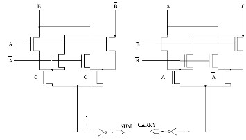
tional description. Adder implementation based on pass tran- sistor principle is shown in Fig.4.
Fig.4.Pass transistor based full adder
Transmission gate approach is another widely used CMOS design style to implement digital function. Transmission gate based implementation is similar to pass transistor with the dif- ference that transmission gate logic uses nMOS and pMOS transistors where as pass transistor logic uses only one type of transistor i.e. either nMOS or pMOS. Full adder implementa- tion based on TG logic is shown in Fig.5. [4]
The sum and carry expressions in (10) have common terms and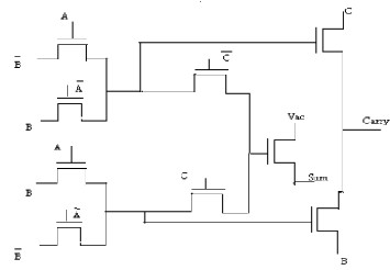
can be implemented using Fig.6. [7]
Fig.6. Pass transistor based adiabatic full adder
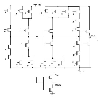
The general PFAL gate consists of a two cross coupled inver- ters and two functional blocks F and /F (complement of F) dri- ven by normal and complemented inputs which realizes both
IJSER © 2011
International Journal of Scientific & Engineering Research Volume 2, Issue 9, September-2011 4
ISSN 2229-5518
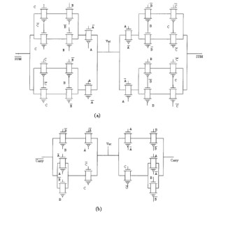
normal and complemented outputs. Both the functional blocks implemented with n channel MOS transistors. The equations used to implement PFAL adder given by (11) and the corres- ponding sum and carry implementations are shown in Fig.7a and Fig.7b![]()
![]()
![]()
![]()
Sum ABC ABC ABC ABC
Carry AB BC CA
(11)
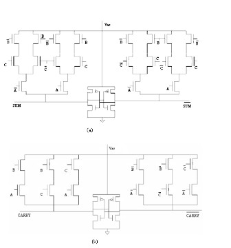
Fig.7.Positive feedback based adiabatic logic a)sum cell b)carry cell
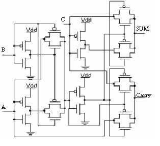
The general block diagram of transmission gate based adiabatic logic consists of two functional blocks F and complement of F operated with single clock power supply. Both normal and complemented inputs are available to functional blocks. Func- tional blocks are implemented using transmission gate or pass gate. The sum and carry implementation using transmission gate logic is shown in Fig .8a and Fig.8b. [4], [11]
In order to estimate the power dissipation of the different cir- cuits present in previous section we used power meter simula- tion model present in [4] and RC model present in [10].All the circuits are designed in Tanner tools(S-edit,T-SPICE) using
0.18um technology parameters.Table.I gives power dissipation values under the operating conditions VDD=1.8V,CL=20fF and frequency 50MHz.Fig.9 shows the variation of power dissipa- tion with the frequency for the different circuit implementa- tions presented in previous section and it confirms that adia- batic logic circuits consume less power than CMOS circuits.
Fig.8. Trasmission gate based adiabatic logic a) sum cell b) carry cell
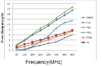
TABLE 1POWER DISSIPATION OF VARIOUS ADDERS UNDER THE OPER- ATING CONDITIONS (VDD=1.8V,CL=20FF,FCLK=50MHZ)
Parameter | Adder type | |||||
Parameter | CMOS | PL | TGL | PAL | PFAL | TGAL |
Transistor count | 28 | 22 | 20 | 10 | 38 | 60 |
Power dissipa- tion(µw) | 1.9 | 1.2 | 2.1 | 0.06 | 0.05 | 0.85 |
Fig.9. variation of power dissipation with frequency
IJSER © 2011
International Journal of Scientific & Engineering Research Volume 2, Issue 9, September-2011 5
ISSN 2229-5518
In this paper we compared the performance of different adia- batic logic adder circuits with traditional CMOS adder circuits. The simulation results show that designs based on adiabatic principle gives superior performance when compared to tradi- tional approaches in terms of power even though their transis- tor count is high in some circuits.
[1] W.C. Athas, L. Svensson, J.G. Koller et ,N.Tzartzanis and E.Y.Chou: “Low- power Digital Systems Bared on Adiabatic-switching Principles”. IEEE Transactions on VLSI Systems. Vol. 2, No. 4, pp. 398-407 December. 1994.
[2] A. Chandrakasan, S. Sheng and R. Brodersen, “Low-power CMOS digital design,” IEEE Journal of Solid State Circuits, Vol. 27, No 4, pp. 473-484, April 1992.
[3] N. Zhuang and H.Wu , “A New Design of the CMOS Full Adder,” IEEE
Journal of Solid-state Circuits, Vol. 27,No. 5, pp 840-844,May 1992.
[4] S.Kang and Y.Leblebici, CMOS Digital Integrated Circuits - Analysis and
Design, Reading chapter 6, McGraw-Hill, 2003.
[5] R K. Navi, Md.Reza Saatchi and O.Daei, “A High-Speed Hybrid Full
Adder,” European Journal of Scientific Research,Vol 26 No.1,pp 29-
33,January 2009.
[6] D. Sourdis, C. Piguet and C. Goutis, “ Designing CMOS Circuits for Low Power, European Low-Power Initiative for Electronic System Design”, Reading pp 71-96, Kluwer Academic Publishers, 2002.
[7] D. Soudris, V. Pavlidis and A. Thanailakis, “Designing Low-Power Energy
Recovery Adders Based On Pass Transistor Logic,” IEEE 2001.
[8] R. Shalem, E. John and L.K. John, “A Novel Low Power Energy Recovery
Full Adder Cell”publisher details unknown
[9] A.G.Dickinson and J.S.Denker, "Adiabatic Dynamic Logic," IEEE Journal of
Solid-state Circuits, Vol. 30 No.3, pp 311-315,March 1995.
[10] M.Alioto and G.Palumbo, “Power Estimation in Adiabatic Circuits: A Simple and Accurate Model”, IEEE Trans on VLSI Systems, VOL. 9, NO. 5, pp 608-615 October 2001.
IJSER © 2011