International Journal of Scientific & Engineering Research, Volume 4, Issue 11, November-2013 1356
ISSN 2229-5518
Clap Switching
Somangshu Bagchi (B.Tech), Subhadip Ghosh (B.Tech), Deepak Nandi (B.Tech)
ABSTRACT
This is a project on CLAP SW ITCH which can switch on/off any electrical circuit by the sound of the clap. The clap-operated circuit is a circuit which operates by clapping from a remote point. W hen a person claps one, the first output of the circuit is turned on. If another one is clapped, the second output is switched on and then another one will cause to energize the third output.
The basic idea of clap switch is that the electric microphone picks up the sound of your claps, coughs, and the sound of that book knocked off the table. It produces a small electrical signal which is amplified by the succeeding transistor stage. Two transistors cross connected as a bistable multivibrator change state at each signal. One of these transistors drives a heavier transistor which controls a lamp. Basically, this is a Sound operated switch.
For example, fan, fluorescent light, TV and other appliances can be switched on (or) off by clapping. This circuit can be used by changing individual situations.
INDEX TERMS
Condenser microphone, BJTs, NE555 Timer, decade counter, LED, relays
——————— ———————
1. INTRODUCTION
A circuited switch, which operates with sound of clapping hands or something similar; i.e. the switch comes to 'on' position when clapped once or twice, and to'off' position when again clapped once or twice (depends on circuit design)
A clap -switch circuit is a sound sensitive circuit. .
The operation of the circuit is simple. Clap and the lamp turns on. Clap again and it turns off. The condenser microphone picks up the sound of your claps, coughs, and the sound of that book knocked off the table. It produces a small electrical signal which is amplified by the succeeding
transistor stage. Two transistors cross connected as a
bistable multivibrator change state at each signal. One of these transistors drives a heavier transistor which controls a lamp. This circuit can switch on and off a light, a fan or a radio etc by the sound of a clap. This working of this circuit is based on amplifying nature of the transistor, switching nature of transistor, relay as an electronic switch .
The LED on-time can be varied by changing the value of the capacitor (100mF). When capacitor value is changed from 100 mF to 10mF, the LED ontime is decreased.
Your clap should be loud, you can blow air from your mouth on the electric condenser to turn on the LED.

Somangshu Bagchi has completed B.Tech in Electronics and Communication from Techno India, Saltlake. He is currently working as an assistant system engineer for Tata Consultancy Services.
Ph No.-+919874194965, E-mail. somangshu282@gmail.com
IJSER © 2013 http://www.ijser.org
International Journal of Scientific & Engineering Research, Volume 4, Issue 11, November-2013 1357
ISSN 2229-5518
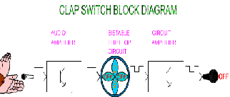
Fig. 1: Clap Switch Block Diagram
An audio power amplifier is an electronic amplifier that amplifies low-power audio signals (signals composed primarily of frequencies between 20 - 20 000 Hz, the human range of hearing) to a level suitable for
driving loudspeakers.
A flip-flop or latch is a circuit that has two stable states and can be used to store state information. A flip-flop is
a bistable multivibrator. Flip-flops and latches are used as data storage elements. Such data storage can be used for storage of state, and such a circuit is described as sequential logic. When used in a finite-state machine, the output and next state depend not only on its current input, but also on its current state (and hence, previous inputs). It can also be used for counting of pulses, and for synchronizing
variably-timed input signals to some reference timing signal.
A bistable circuit has two stable states. The output of a bistable can be either logic1 or logic 0, according to signals received at the inputs. One of the simplest bistable circuits
consists of two NAND gates.
2. METHODOLOGY:
2.1 PROBLEM DEFINITION:
Our objective is to develop a switch which will recognize two intense sounds within a interval of 3 seconds.
2.2 PLANNING AND APPROACH:
First we take a condenser microphone that senses the sound of the clapping. Next is the amplifying stage that will amplify the sound received from the microphone. Two ICs have been used. The first one senses the first clap and the output of which gives power to the second IC. The second IC is activated by the second clapping sound and its output is fed to the relay which switches on the load when output from the second IC is received.
PLANNING:
1.1 PROJECT OBJECTIVE:
This objective of the project is to design a clap activated switch device that will serve well in different phono- controlled applications, providing inexpensive key and at the same time free from false triggering. This involves the design of various stages consisting of the pickup transducer, low frequency, audio low power and low noise amplifier, timer, bistable multivibrator and switches. It also
consists of special network components to prevent false
APPROACH:
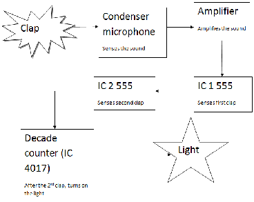
Fig. 2: Block Diagram
triggering and ensure desired performance objectives. A
decade counter IC serves the bistable function instead of flip-flop.
• The condenser microphone will capture the sound and convert it into an electric signal.

Somangshu Bagchi has completed B.Tech in Electronics and Communication from Techno India, Saltlake. He is currently working as an assistant system engineer for Tata Consultancy Services.
Ph No.-+919874194965, E-mail. somangshu282@gmail.com
IJSER © 2013 http://www.ijser.org
International Journal of Scientific & Engineering Research, Volume 4, Issue 11, November-2013 1358
ISSN 2229-5518
• Hand claps are typically within the 2200 to 2800 hertz range.
• The 2nd stage amplifier will enlarge the signal which will help the 1st 555 timer to recognize the 1st clap.
• Now, if a 2nd clap is recognized by the 2nd 555 timer within an interval of 3 secs. Then the
switch will trigger the device and move to ON
state.
• The decade counter is there to check if the two claps are generated within 3 seconds.
2.2.1 PROJECT DESIGN:
Input Stage :
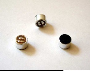
Fig. 3: Condenser Microphone (Transducer)
The sound of your claps is picked up using a condenser microphone. This microphone has a stage of amplification built in. The power for this built in amplifier is supplied by connecting a resistor to a positive source of voltage, and the changes in current get reflected as changes in voltage across this resistor according to the familiar relation V = I*R. A larger resistor will give you a larger voltage, but then, the current into the device gets reduced which brings down the gain. The value of 5600 ohms (usually abbreviated to 5.6K, and written down in schematics as 5K6) seems to work all right.
Amplifier Stage:
A transistor stage, biased near cut-off amplifies the signal from the microphone. The output of the microphone is coupled to the base of the transistor using an electrolytic capacitor (note: using a better capacitor here will not work). The first time the microphone output goes positive, however, (because somebody clapped) this change gets coupled to the base entirely due to the action of the capacitor. This causes the current through the transistor to increase, and this increase in current causes the voltage at the collector, which was sitting near the supply voltage, to fall to nearly zero. This is not a high fidelity audio
amplifier. Its function is to produce no output for small
sounds and large output for (slightly) bigger sounds, so the customary biasing network can be omitted.
Bistable Multivibrator Stage:
Two cross connected transistors in a bistable multivibrator arrangement make up a circuit that remembers. You can set it to one of two possible states, and it will stay in that state until the end of time. When one transistor conducts, its collector is near ground, and a resistor from this collector feeds the base of the other. Since this resistor sees ground at the collector end the base at the other end receives no current, so that transistor is off. Since this transistor is off,
its collector is near supply potential and a resistor connects from this to the base of the other transistor. Since this resistor sees voltage, it supplies the base with current, ensuring that the transistor remains on. Thus this state is stable. By symmetry, the other state is, too. e.g IC555
IC555 Timer
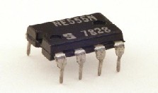
Fig. 4: IC-555 Timer
The 8-pin 555 timer must be one of the most useful ICs ever made and it is used in many projects. With just a few external components it can be used to build many circuits, not all of them involve timing. A popular version is the

Somangshu Bagchi has completed B.Tech in Electronics and Communication from Techno India, Saltlake. He is currently working as an assistant system engineer for Tata Consultancy Services.
Ph No.-+919874194965, E-mail. somangshu282@gmail.com
IJSER © 2013 http://www.ijser.org
International Journal of Scientific & Engineering Research, Volume 4, Issue 11, November-2013 1359
ISSN 2229-5518
NE555 and this is suitable in most cases where '555 timer' is specified. Low power versions of the 555 are made, such as the ICM7555, but these should only be used when specified (to increase battery life) because their maximum output current of about 20mA (with a 9V supply) is too low for many standard 555 circuits. The ICM7555 has the same pin arrangement as a standard 555.The circuit symbol for a 555 is a box with the pins arranged to suit the circuit diagram: for example 555 pin 8 at the top for the +Vs supply, 555 pin
3 output on the right. Usually just the pin numbers are used
and they are not labeled with their function. The 555 can be
used with a supply voltage (Vs) in the range 4.5 to 15V (18V
absolute maximum).Standard555 ICs create a significant
'glitch' on the supply when their output changes state. This
is rarely a problem in simple circuits with no other ICs, but in more complex circuits a capacitor (eg. 100µF) should be connected across the +Vs and 0V supply near the 555.
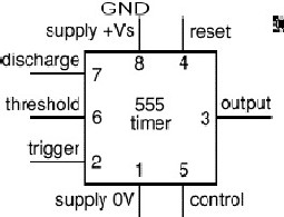
Fig. 5: Pinout Diagram
Trigger input
When <1/ 3 Vs ('active low') this makes the output high (+Vs). It monitors the discharging of the timing capacitor in an a stable circuit. It has a high input impedance > 2M.
Threshold input
When >2 / 3 Vs ('active high') this makes the output low (0V). It monitors the charging of the timing capacitor in a stable and monostable circuits. It has a high input impedance > 10Mproviding the trigger input is >1 / 3 Vs, otherwise the trigger input will override the threshold input and hold the output high (+Vs).
Reset input
When less than about 0.7V ('active low') this makes the output low (0V), overriding other inputs. When not required it should be connected to +Vs. It has an input impedance of about 10k.
Control input
This can be used to adjust the threshold voltage which is set internally to be 2 / 3 Vs. Usually this function is not required and the control input is connected to 0V with a0.01µF capacitor to eliminate electrical noise. It can be left unconnected if noise is not a problem.
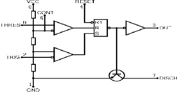
Fig. 6: Internal Circuit of 555 Timer
Modes of 555 Timer
MONOSTABLE

Somangshu Bagchi has completed B.Tech in Electronics and Communication from Techno India, Saltlake. He is currently working as an assistant system engineer for Tata Consultancy Services.
Ph No.-+919874194965, E-mail. somangshu282@gmail.com
IJSER © 2013 http://www.ijser.org
International Journal of Scientific & Engineering Research, Volume 4, Issue 11, November-2013 1360
ISSN 2229-5518
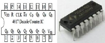
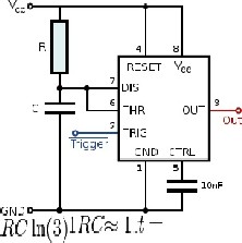
Fig. 7: Schematic of a 555 in monostable mode
The relationships of the trigger signal, the voltage on C and the pulse width in monostable mode. In the monostable mode, the 555 timer acts as a “one-shot” pulse generator. The pulse begins when the 555 timer receives a signal at the trigger input that falls below a third of the voltage supply. The width of the output pulse is determined by the time constant of an RC network, which consists of a capacitor(C) and a resistor(R). The output pulse ends when the voltage on the capacitor equals 2/3 of the supply voltage. The output pulse width can be lengthened or shortened to the need of the specific application by adjusting the values of Rand C. The output pulse width of time t, which is the time it takes to charge C to 2/3 of thesupply voltage, is given by
t=RCln(3)=1.1RC (approx.)
where t is in seconds, R is in ohms and C is In farads.. While using the timer IC as a monostable, the main disadvantage is that the time span between the two triggering pulses must be greater than the RC time constant
BISTABLE
In bistable mode, the 555 timer acts as a basic flip-flop. The trigger and reset inputs (pins 2and 4 respectively on a 555) are held high via Pull-up resistors while the threshold input (pin6) is simply grounded. Thus configured, pulling the trigger momentarily to ground acts as a 'set' and transitions the output pin (pin 3) to Vcc (high state). Pulling the reset input to ground acts as a 'reset' and transitions the output pin to ground (low state). No capacitors are required in a bistable configuration. Pin 5 (control) is connected to
ground via a small-value capacitor (usually 0.01 to 0.1 uF);
pin 7 (discharge) is left floating.
Decade Counter (CD4017IC):
4017 IC is a common useful digital IC. [ From input pin (14 nodes)]. This is called divided by10 counter because it produces one tenth of square wave frequency provided from input pin(pin 14) to output pin (on pin 12).Counter circuit is a digital circuit. Generally, counter is the circuit that counts the number of the square wave entered to the circuit. In CD 4017 IC means the symbol of the company
that produces the IC. There are IC, with other letters, this IC
is called 4017 IC is the form of 14 pin DIP which includes 16
pins. Block diagram of IC pin and the application of IC are shown in Figure (a) and (b) respectively. The function of each pin is shown in the following:
Fig. 8: Pinout Diagram of CD4017 IC
INPUT PINS
CLK-clock input (pin 14) Pin 14 is input which is connected with the square wave. If 10V is supplied to IC, the frequency of the input square wave must be below 5MHz. Similarly, the supplied voltage is5V, the frequency of the input square wave must be below 2.5 MHz.
En- clock Enable input (pin13) Pin 13 is grounded to alternate the high-state of the output pin (Qo - Q9) of 4017
ICregularly. If pin 13 is connected to positive supply, the counter will stop.
R- Reset input (pin 15) Pin 15 is grounded to alternate the high-state of the output pin (Qo - Q9). In practice, pin15 is connected to the positive supply and time directly reconnected to the ground to reset it.
VDD, VSS Supply pins (pin 16 and pin 18) Pin 16 is connected to the positive supply and illustrated with VDD. Pin18 is the pin to be connected to the ground is described with VSS.
OUTPUT PINS
Q0 – Q9 The output pins are from Q0 to Q9. When the square wave is supplied to input pin 14, each pin from Q0 to Q9 changes to high state in its every positive going edge. Only one of the 10 output pins is in high-state and other 9 output pins are all low-sate.CO- Carry Out CO is also output pin. But, the frequency of square wave from output pin is one tenth of the frequency supplied from pin 14.
CD 4017 IC Specification Supplied voltage 3V–15V Max: out current 10mA Max
Power absorbed by each pin 100 Mw

Somangshu Bagchi has completed B.Tech in Electronics and Communication from Techno India, Saltlake. He is currently working as an assistant system engineer for Tata Consultancy Services.
Ph No.-+919874194965, E-mail. somangshu282@gmail.com
IJSER © 2013 http://www.ijser.org
International Journal of Scientific & Engineering Research, Volume 4, Issue 11, November-2013 1361
ISSN 2229-5518
4017 IC can work very well with supplied voltage 3V to 5V. Although the maximum supplied voltage is 15V, practically only 12V usually used.
The counting action of the 4017 can be understood from the graph below:
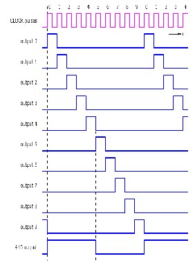
Fig. 9: Timing Diagram
Transistor BC 548/549:
As a representative of the large family of bipolar transistors the BC548 provides a "steppingoff point" to the use of more esoteric, higher voltage, current or frequency devices forbeginners.If theTO-92package is held in front of one's face with the flat side facing towardyou and the leads downward, (see picture) the order of the leads, from left to right is collector, base, emitter.
The BC548/549 transistor is an NPN Epitaxial Silicon Transistor. The BC547transistor is a general-purpose transistor in a small plastic package. It is used in general- purpose switching and amplification BC548/BC549 series
45 V, 100 mA NPN general-purpose transistors.
The BC548/549 transistor is an NPN bipolar transistor, in which the letters "N" and "P" refer to the majority charge carriers inside the different regions of the transistor. Most bipolar transistors used today are NPN, because electron mobility is higher than hole mobility in semiconductors, allowing greater currents and faster operation. NPN transistors consist of a layer of P-doped semiconductor (the "base") between two N-doped layers. A small current entering the base in common-emitter mode is amplified in the collector output. In other terms, an NPN transistor is "on" when its base is pulled high relative to the emitter. The arrow in the NPN transistor symbol is on the emitter leg and points in the direction of the conventional current flow when the device is in forward active mode. An NPN transistor can be considered as two diodes with a shared anode region. In typical operation, the emitter base junction is forward biased and the base collector junction is reverse biased. In an NPN transistor, for example, when a positive voltage is applied to the base emitter junction, the equilibrium between thermally generated carriers and the repelling electric field of the depletion region becomes unbalanced, allowing thermally excited electrons to inject into the base region. These electrons wander (or "diffuse")
through the base from the region of high concentration near
the emitter towards the region of low concentration near the collector. The electrons in the base are called minority carriers because the base is doped p-type which would make holes the majority carrier in the base.
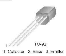
Fig. 10: NPN transistor

Somangshu Bagchi has completed B.Tech in Electronics and Communication from Techno India, Saltlake. He is currently working as an assistant system engineer for Tata Consultancy Services.
Ph No.-+919874194965, E-mail. somangshu282@gmail.com
IJSER © 2013 http://www.ijser.org
International Journal of Scientific & Engineering Research, Volume 4, Issue 11, November-2013 1362
ISSN 2229-5518
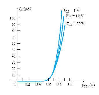
Fig. 11: BC548/549 and its input characteristics
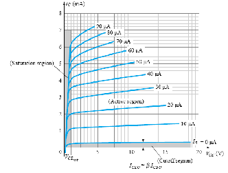
Fig. 12: Output characteristics of BC548/549
In the active region of a common-emitter amplifier the collector-base junction is reverse-biased, while the base- emitter junction is forward-biased.
2.2.2 A GENERAL DESCRIPTION OF THE COMPONENT USED:
1. Condensor Microphone
A microphone is an acoustic-to-electric transducer or sensor that converts sound into an electrical signal. The condenser microphone, invented at Bell Labs in 1916 by E. C. Wente is also called a capacitor microphone or electrostatic microphone. Here, the diaphragm acts as one plate of a capacitor, and the vibrations produce changes in the distance between the plates. The voltage maintained across the capacitor plates changes with the vibrations in the air, according to the capacitance equation (C = Q / V), where Q = charge in coulombs, C = capacitance in farads and V = potential difference in volts. The capacitance of the plates is inversely proportional to the distance between them for a
parallel-plate capacitor.
2. Resistor (R)
A component is used for its resistance. In the past, most resistors were manufactured from carbon composition, a baked mixture of graphite and clay. These have been almost completely superseded by carbon or metal film resistor. Wire-wound resistors are used for comparatively low values of resistance where precise value is important, or for high dissipation. They are unsuitable for RF use because of their reactance.
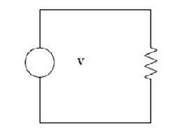
Fig. 13: Resistive Network
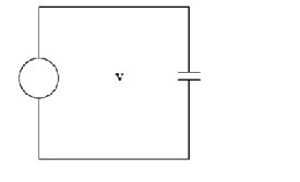
3. Capacitor (C)
A passive circuit component is a capacitance. A capacitor is formed from a pair of conducting surfaces separated by a layer of insulator. A capacitor made from a pair of parallel

Somangshu Bagchi has completed B.Tech in Electronics and Communication from Techno India, Saltlake. He is currently working as an assistant system engineer for Tata Consultancy Services.
Ph No.-+919874194965, E-mail. somangshu282@gmail.com
IJSER © 2013 http://www.ijser.org
International Journal of Scientific & Engineering Research, Volume 4, Issue 11, November-2013 1363
ISSN 2229-5518
conducting plates of area S separated by a distance d, with the gap between the plates filled by a dielectric of relative permittivity E, will have a capacitance C given by
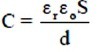
where εo is the permittivity of free space.
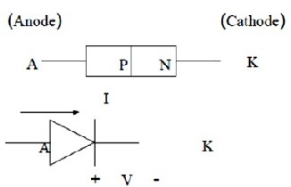
Fig. 15: Symbol of a Diode
5. Bipolar Junction Transistor
Fig 14: Capacitive Network
4. Diode (D)
Diode can be made of either two of semiconductor materials, silicon and germanium. Power diodes are usually constructed using silicon and germanium. Silicon diode can operate at higher current and at higher junction temperature, and they have greater reverse resistance. The structure of a semiconductor diode and it symbol are shown in Figure. The diode has two terminals, an anode, A terminal ( P junction ) and a cathode K terminal ( N junction ). When the anode voltage is more positive than the cathode, the diode is said to be forward biased and it
conducts current readily with a relatively low voltage drop.
When the cathode voltage is more positive than the anode,
the diode is said to be reverse biased, and it blocks current
flow. The arrow on the diode symbol shows the direction of convection current flow when the diode conducts.
A multi electrode semiconductor device in which the current flowing between two specified electrons is controlled or modulated by the voltage applied at third (control) electrodes. The term transistor was originally derived from the phase transfer resistor, as the resistance of the output electrode was controlled by the input circuit. Transistors fall into twomajor classes: the bipolar junction transistor (BJT) and the field-effect transistor (FET).We used bipolar junction transistor (BJT).Bipolar junction transistor consists of (a) pnp transistor and (b) npn transistor.
(a) pnp transistor
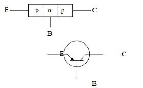
Fig. 16: pnp transistor circuit symbol
In a pnp transistor, a thin layer of n-type semiconductor is sandwiched between two layers of p-type semiconductor.

Somangshu Bagchi has completed B.Tech in Electronics and Communication from Techno India, Saltlake. He is currently working as an assistant system engineer for Tata Consultancy Services.
Ph No.-+919874194965, E-mail. somangshu282@gmail.com
IJSER © 2013 http://www.ijser.org
International Journal of Scientific & Engineering Research, Volume 4, Issue 11, November-2013 1364
ISSN 2229-5518
(b) npn transistor
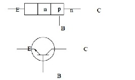
Fig. 17: npn transistor circuit sysmbol
5. RELAY
Relays are one of the oldest, simplest, and yet, easiest and most useful devices. Before the advent of the mass produced transistor, computers were made from either relays or vacuum tubes, or both. A relay, quite simply, is a small machine consisting of an electromagnet (coil), a switch, and a spring. The spring holds the switch in one position, until a current is passed through the coil. The coil generates a magnetic field which moves the switch. It's that simple. You can use a very small amount of current to activate a relay, and the switch can often handle a lot of current. The relay we are going to look at is the Bosch 5 pin relay. Bosch is a German manufacturing conglomerate
(who also happen to own Bosch Telekom and Blaupunkt),
but they are not the only manufacturer of this relay. There
are several other companies such as Siemens (stop laughing) and Potter & Brumfield. The Bosch 5 pin relay is the most widely usedand versatile relay, and it can handle up to 30 amps, which is more than suitable for most applications.
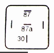
Fig 18: Pinout of Relay
Looking at the diagram to the right, we see the pin out of the relay. Note that each pin is numbered, 85, 86, 87, 87a, and 30. The 30 pin is set perpendicular to the other pins to let you know where each pin is at (although, most relays are labeled at the bottom). 85 and86 are the coil pins. Normally, it doesn't matter which way you pass the current, because if you hook it up backwards, the coil will still activate the relay. However, relays sometimes have an odd tendency to turn themselves back on briefly. To counter this, a diode (a one way switch) is placed between
85 and 86.This is referred to as a tamping diode.
A diode wall have a very high resistance in one direction, and a very low resistance in the opposite direction. When a tamping diode is used, it is important that you hook the coil up according to polarity. If a tamping diode is used, and
you hook it up backwards, you will essentially be shorting a wire out, which sucks, because you can and will burn something up.
30, 87, and 87a are the other three pins. 87 and 87a are the two contacts to which 30 will connect. If the coil is not activated, 30 will always be connected to 87a. Think of that pin as"87, always connected". When current is applied to the coil, 30 is connected to 87. 87 and87a are never connected to each other. Here, polarity does not ever matter. You can connect30 up to positive or negative, and that is what you will get out of 87 or 87a. As you can see, the coil is in no way connected to the switch part of the relay. This can allow you to completely isolate one circuit from another. You can even use a separate power supply to control the relay.
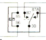
Fig. 19: Diagram of Relay

Table 1:Items and Components Details:
Item Name Value/Details Quantity

Somangshu Bagchi has completed B.Tech in Electronics and Communication from Techno India, Saltlake. He is currently working as an assistant system engineer for Tata Consultancy Services.
Ph No.-+919874194965, E-mail. somangshu282@gmail.com
IJSER © 2013 http://www.ijser.org
International Journal of Scientific & Engineering Research, Volume 4, Issue 11, November-2013 1365
ISSN 2229-5518
CIRCUIT DESIGN:
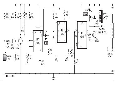
Fig. 20: Circuit Diagram of Clap Switch
CIRCUIT OPERATION:
The clap sound sensed by condenser microphone is amplified by transistor T1. The amplified signal provides negative pulse to pin 2 of IC1 and IC2, triggering both the ICs. IC1, commonly used as a timer, is wired here as a monostable multivibrator. Triggering of IC1 causes pin 3 to go high and it remains high for a certain time period depending on the selected values of R7 and C3. This ‘on’ time (T) of IC1 can be calculated using the following relationship: T=1.1R7.C3 Seconds where R7 is in ohms and C3 in microfarads. On first clap, output pin 3 of IC1 goes high and remains in this standby position for the preset time. Also, LED1 glows for this period. The output of IC1 provides supply voltage to IC2 at its pins 8 and 4.Now IC2 is ready to receive the triggering signal. Resistor R10 and capacitor C7 connected to pin 4 of IC2 prevent false triggering when IC1 provides the supply voltage to IC2 at
first clap.
3. CIRCUIT DESIGN AND CIRCUIT OPERATION:
On second clap, a negative pulse triggers IC2 and its output pin 3 goes high for a time period depending on R9 and C5.This provides a positive pulse at clock pin 14 of
decade counter IC 4017 (IC3). Decade counter IC3 is wired

Somangshu Bagchi has completed B.Tech in Electronics and Communication from Techno India, Saltlake. He is currently working as an assistant system engineer for Tata Consultancy Services.
Ph No.-+919874194965, E-mail. somangshu282@gmail.com
IJSER © 2013 http://www.ijser.org
International Journal of Scientific & Engineering Research, Volume 4, Issue 11, November-2013 1366
ISSN 2229-5518
here as a bistable. Each pulse applied at clock pin 14 changes the output state at pin 2 (Q1) of IC3 because Q2 is connected to reset pin 15. The high output at pin 2 drives transistor T2 and also energises relay RL1. LED2 indicates activation of relay RL1 and on/off status of the appliance. A free-wheeling diode (D1) prevents damage of T2 when relay de-energises.
4. RESULTS AND DISCUSSION:
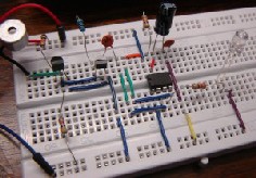
Fig. 21: When the battery is not connected
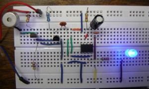
Fig. 22: When the battery is connected
During the practical implementation of the project, some of the values or components had to be changed in order to get more accurate result. The circuit was first performed on bread board and only after successful implementation and satisfied output, it was built on a vero board.
1. In the output, a bulb is used instead of an LED.
A red LED is used to indicate the first clap. When the first NE 555 timer generates the output, the LED glows.
2. A 12 volts power supply has been used instead of the
9 volts power supply to get satisfied results.
3. The relay can drive any common home electrical appliance like fan, light, television etc.
The time period of the pulse applied as the power supply of the IC 2(second NE 555 timer) is calculated by the formula:
T = 1.1 x R7 x C3
According to the theoretical values, the time period should be:
T = 1.1 x 270k x 10u
=2.97
But the practical value of T in this circuit is 3.20 seconds which is slightly greater than the calculated theoretical output. This is due to the tolerance of the components used in the circuit.
5. CONCLUSION
Assemble the circuit on a general-purpose PCB and enclose it in a suitable box. This circuit is very useful in field of electronic circuits. By using some modification it area of application can be extended in various fields. It can be used to raised alarm in security system with a noise, and also used at the place where silence needed.
This project gives us a great deal of knowledge about the
555 timer chips, working of clocks and the relay. This type of device provides us with the working of NE555 timer chips and the relay. The relay is a type of switch which provides a conducting path only when current flows it. In this project as soon as the 2nd timer triggers the relay a conducting path is established between terminals of the load and hence the device is turned on. The time interval between the claps is judged with the time constant
established with the RC configuration which is T=1.1R7*C3.

Somangshu Bagchi has completed B.Tech in Electronics and Communication from Techno India, Saltlake. He is currently working as an assistant system engineer for Tata Consultancy Services.
Ph No.-+919874194965, E-mail. somangshu282@gmail.com
IJSER © 2013 http://www.ijser.org
International Journal of Scientific & Engineering Research, Volume 4, Issue 11, November-2013 1367
ISSN 2229-5518
This switch is very low cost and is very useful to the elderly and physically challenged people. But the major disadvantage of this switch is false triggering. The switch can be triggered by any two sounds similar to that of hands clapping. So care has to be taken to avoid this kind of false triggering and the switch should not be used in very sensible applications. It is only for home uses.
But nevertheless it is an excellent example of electronics evolution and how engineering and electronics have made our life easier.
ADVANTAGES AND APPLICATIONS: ADVANTAGES:
1. Energy efficient
2. Low cost and reliable circuit
3. Complete elimination of manpower
4. High Accuracy
APPLICATIONS:
The major advantage of a clap switch is that you can turn something (e.g a lamp) on and off from any location in the room (e.g while lying in bed) simply by clapping your hands.
The primary application involves an elderly or mobility- impaired person. A clap switch is generally used for a light, television, radio or similar electronic device that the person will want to turn on/off from bed.
The major disadvantage is that it is generally cumbersome to have to clap one’s hands to turn something on or off and it is generally seen as simpler for most use cases to use a traditional light switch.
There is a further scope of work on this project. This circuit can be made more accurate and more sensible to suit the practical use in our daily lives.
FUTURE SCOPE
No filter has been used here so the switch will respond to more or less every two sounds similar to clapping that comes with a gap of in between 3 seconds. But if a simple bandpass filter is used then this problem could be avoided. The frequency range of hand clapping is in between 2200 and 2800 Hertz.
Here the signal from the condenser mic is beta times amplified by the amplifier stage. To add more sensitivity to the switch, the amplification factor may be
increased.
Unconventional Uses for IC Timers” Jim Wyland and
Eugene Hnatek,
Electronic Design, June 7, 1973, pp. 88-90.
DC-to-DC Converter Uses the IC Timer”, Robert Soloman and Robert
Broadway, EDN, September 5, 1973, pp. 87-91.
Books:
[1] Robert L. Boylestad and Louis Nashelsky, Electronics devices and circuit theory, ninth edition.
[2] Millman and Halkias, Electronics devices and circuit theory.

Somangshu Bagchi has completed B.Tech in Electronics and Communication from Techno India, Saltlake. He is currently working as an assistant system engineer for Tata Consultancy Services.
Ph No.-+919874194965, E-mail. somangshu282@gmail.com
IJSER © 2013 http://www.ijser.org
International Journal of Scientific & Engineering Research, Volume 4, Issue 11, November-2013 1368
ISSN 2229-5518

Somangshu Bagchi has completed B.Tech in Electronics and Communication from Techno India, Saltlake. He is currently working as an assistant system engineer for Tata Consultancy Services.
Ph No.-+919874194965, E-mail. somangshu282@gmail.com
IJSER © 2013 http://www.ijser.org