International Journal of Scientific & Engineering Research, Volume 5, Issue 6, June-2014 81
ISSN 2229-5518
Carrier Based Hybrid PWM Algorithm With Reduced Common Mode Voltage For Three Phase Voltage Source Inverter Fed Vector Controlled Induction Motor Drives
A Pradeep B Jyoti
E.E.E. Department
RYM Engineering college, Bellary, Karnataka, India pradeepbjyoti@gmail.com
J. Amarnath, Professor
E.E.E. Department
JNTUH College of Engineering, Hyderabad, Andhra Pradesh, India amarnathjinka@yahoo.com
D. Subba Rayudu, Rtd. Professor, E.E.E. Department,
G.Pulla Reddy Engineering college, Kurnool, Andhra Pradesh, India
dr-subbarayudu@yahoo.co.in
voltage vectors, the common mode voltage variations can be minimized from
± Vdc
![]()
2 to
![]()
± Vdc 6
when compared with the SVPW M algorithm.
Furthermore, the rms flux ripple which is a measure of current ripple characteristics are plotted for all the sequences of AZSPW M algorithm. Then, in each sampling time period, the suitable sequence, which gives reduced common mode voltage, is applied to obtain the HAZSPW M algorithm. To evaluate the proposed algorithm simulation studies have been carried on vector controlled induction motor drive and the results are presented. The results show good agreement with the proposed work.
I. INTRODUCTION
The Pulsewidth Modulated Voltage Source Inverter (PWMVSI) fed Variable Speed Drives (VSD) are increasingly used in many industrial, traction and electric vehicle applications. Due to the recent advancements in the fast switching semiconductor technology, pulsewidth modulation methods are of growing interest to achieve the variable voltage and variable frequency ac supply.
In the traditional days, the variable speed drive applications are mainly based on dc motors. After the
and excellent dc bus utilization [6]. In SVPWM algorithm, the switching times are calculated based on the magnitude of the reference. Though this algorithm gives out superior waveform quality, it gives more switching losses and harmonic distortion at higher modulation indices. In order to obtain superior waveform quality at higher modulation indices, the Discontinuous PWM (DPWM) techniques are proposed [7 - 9]. A hybrid PWM technique is presented in [8] combining DPWM and SVPWM at all modulation indices by using stator flux ripple concept. But, at all modulation indices SVPWM and DPWM algorithms give large amount of
invention of vector control or Field oriented control (FOC)
algorithm, induction motors are becoming popular in
Common Mode Voltage (CMV) variations between
due to the presence of zero states.![]()
± Vdc 2
controlling the drive system. In FOC, the control of induction motor is similar to separately excited dc motor [1]. By using digital signal processor and power electronic converters, much advancement has been made in the vector control algorithm which is explained [2-4]. Due to the requirement of variable voltage and variable frequency, the usage of PWM algorithms is mandatory for the control. A detailed survey of newly developed PWM algorithms which are different in concept and performance are described in [5]. Compared with the sinusoidal modulation, the PWM method based on the voltage space vectors result in reduced harmonic distortion
Moreover, with the increase in CMV, the Common
Mode Current (CMV) flows through the winding which cause
bearing problems and early mechanical failure of the machine [10-11]. In the traditional days, the effect of CMV and CMC is reduced using passive and active filters which are explained in detail in [12]. But, the active and passive filters require power electronic converter, inductor and capacitor which increase the cost and also require additional hardware.
In the recent years, many researchers are focusing
their interest on the development of various reduced CMV PWM algorithms without the requirement of additional
IJSER © 2014 http://www.ijser.org
International Journal of Scientific & Engineering Research, Volume 5, Issue 6, June-2014 82
ISSN 2229-5518
equipment [13-17]. The detailed study of various Reduced
Common Mode Voltage PWM (RCMVPWM) algorithms is given in [14]. The PWM algorithms, which are used for the reduction of CMV variations, may be classified into three categories such as Active Zero State PWM (AZSPWM), Remote State PWM (RSPWM) and Near State PWM (NSPWM) algorithms. The AZSPWM algorithm gives reduced common mode voltage of the inverter but the total harmonic distortion is more.
The generation of pulse pattern using the classical space
V
o V V
V
Induction Motor
Z
n
V
vector approach requires sector and angle information which
increases the complexity. To minimize the burden, a simple
carrier comparison approach is explained in [10-13]. It
involves the generation of modulating signals using the voltage magnitude tests. However, in this approach the
selection of the carrier wave is region dependent.
This paper first presents a simple scalar approach for the generation of different PWM techniques such as SVPWM, AZSPWM, NSPWM and DPWM algorithms. Then, by utilizing the concept of stator flux ripple, the rms stator flux ripple characteristics are plotted, from which finally HAZSPWM techniques using flux ripples are presented with reduced common mode voltage and lesser harmonic distortion. Moreover, this algorithm is applied for the vector control of induction motor.
A. Principle of Carrier Comparison Approach
Volt-Second balance is the most commonly used principle for all the PWM algorithms. According to this principle, the generation of the required reference voltage has to be done within a sampling time period. The principle of the carrier comparison approach involves the comparison of the triangular (carrier) signal with the modulating signal of a, b, c
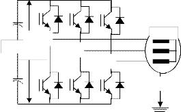
Fig. 1 Two-level inverter fed induction motor drive
In order to maintain the constant position of the pulse, a zero sequence voltage can be added to the sinusoidal signals which do not affect the average value of the line voltage. But, due to the change in the pulse position, switching frequency characteristics and the harmonic properties will be affected. Infinite number of PWM algorithms can be obtained by adding a suitable zero sequence signal to the sinusoidal signals. Based on the proper zero sequence signal, the SVPWM and various DPWM, AZSPWM and NSPWM algorithms can be derived in a simple form.
B. Proposed Scalar Appraoch
The classical space vector approach which is explained in [2] requires the sector and angle information which increases the calculation burden. For simplicity, a scalar (carrier) approach is presented in this paper. So, in the proposed approach, the calculation of zero sequence signal is carried out using voltage magnitude test. Then, the modulating signal can be generated by adding the zero sequence signal to the reference phase voltage.
The set of instantaneous reference phase voltages can be assumed as
Vin = Vref cos(θ - 2(r - 1)π ![]() 3)
3)
phases. The intersection point of both the waveforms give the
switching instant of the switches. Out of the two switches of
for i = a, b, c and r = 1,2,3
(1)
each leg of the inverter, at any instant either the top or bottom switch will conduct. The derivation of the fundamental output voltage depends on shape of modulating signal. In a
The calculated unique zero sequence signal ( Vzs ) based on the voltage magnitude tests is given in (2).
sinusoidal PWM (SPWM) technique, three sinusoidal signals,
which are shifted by 120o are compared with a common
triangular signal for the generation of gating pulses. This
Vzs
![]()
= Vdc
2
(2ko
− 1) −
koVmax
+ (ko
− 1)Vmin
(2)
technique is most commonly used for variable speed drive
The maximum and minimum values of Vin are represented as
applications. But, the line current in SPWM algorithm gives
more harmonic distortion. In a 3-phase VSI with isolated
Vmax and
Vmin . By adding this zero sequence signal to the
*
neutral point of the load, the voltage between the neutral point
Vin , the modulating waves ( Vin ) are derived as given in (3).
and midpoint of the dc bus ( Vno ), which is also known as
V * = V + V
(3)
CMV as shown in Fig. 1 can be varied freely.
in in zs
The variation of the constant
k o between 0 and 1, the
modulating signals for various PWM techniques such as SVPWM, AZSPWM, NSPWM and DPWM algorithms can be generated. In this paper, the main demonstration is regarding AZSPWM algorithms due to the absence of zero states in the switching sequence. But the modulating waveforms of
IJSER © 2014 http://www.ijser.org
International Journal of Scientific & Engineering Research, Volume 5, Issue 6, June-2014 83
ISSN 2229-5518
SVPWM and AZSPWM are similar due to which the constant k o value is fixed as 0.5. however, this paper mainly focuses on AZSPWM algorithms only.
In general carrier approach, the generated modulating waveforms are compared with a common triangular waveform to generate the pulse pattern. But, AZSPWM algorithms require, two triangular signals (Vtri and –Vtri )
which are in phase opposition with each other. Then, by
changing the polarity of the triangular signals different
AZSPWM algorithms such as AZSPWM1, AZSPWM2 and AZSPWM3 can be generated. The following procedure can be used to change the polarity of the carrier signals.
The generation of for AZSPWM1, AZSPWM2 and
AZSPWM3 techniques involves the three sets of 3-phase
voltages are assumed as given in (4)-(6) respectively. These signals are used as test signals for the comparison with
The modulating signals, carrier signals and
corresponding pole voltage and CMV for SVPWM and
proposed AZSPWM algorithms are shown in Fig. 3 - Fig. 6. From these, it can be observed that the proposed AZSPWM algorithms did not use the zero states. The voltage of neutral point of the load with respect to the midpoint of the dc bus is defined as CMV and is shown in Fig. 1. This can be represented as given in (7).
Vao + Vbo + Vco
triangular waves.
Vix = Vref cos(θ - 2(r - 1)π ![]() 3)
3)
![]()
Vno = Vcom = 3
(7)
(4)
As per (7), the CMV of SVPWM may take a value of
for i = a, b, c and r = 1,2,3
![]()
± Vdc 2
due to the usage of zero states. But, the AZSPWM
Viy = Vref cos(θ - 2(r - 1)π![]()
3 + 2π / 3)
(5)
algorithms may take a value of
± Vdc
![]()
6 . Thus, by using the
for i = a, b, c and r = 1,2,3
AZSPWM algorithms, the CMV variations and hence CMC
can be reduced.
Viz = Vref cos(θ - 2(r - 1)π ![]()
![]()
3 − 2π 3)
(6)
for i = a, b, c and r = 1,2,3
The change in polarity of carrier signals depends on the region. For all AZSPWM algorithms, the corresponding modulating signal of that phase will be compared with the
+Vtri if the slope of the corresponding test signal is positive.
Similarly, if the slope of the test signal is negative then the
A. Analysis of Stator Flux Ripple
The measurement of the waveform quality generated by a PWM inverter is defined as the total harmonic distortion (THD) of a line current. It is given by
modulating signal of that phase will be compared with the -
Vtri. After observing the obtained pulse pattern, the sequences![]()
I ITHD = I
∑ I 2
(8)
of AZSPWM are shown in table.1. Also, the block diagram of
1 n≠1
proposed scalar approach is as shown in Fig. 2.
where, I1 and I n
are the rms values of the fundamental and
Vin
Vix
Zero sequence
Calculation
+
+ +
Carrier signal - generation
the nth harmonic components of the no-load current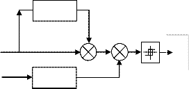
respectively.
All the AZPWM methods maintain volt-seconds balance
to generate a voltage space vector, which equals to reference Sa space vector in an average sense. The difference between the Sb applied voltage vector and reference voltage is the ripple Sc voltage vector. The error volt-seconds corresponding to ripple voltage vectors can be developed as given in [13]. For the
AZPWM sequences the d-axis stator flux ripple components
Fig. 2 Proposed scalar approach
are given in terms of D,P,S and R and q-axis stator flux ripple
TABLE.1 REGION DEPENDENT SWITCHING SEQUENCES FOR
components are given in terms of
Q1 , Q2 , Q 3 , Q5 , Q 6 ,
VARIOUS AZSPWM ALGORITHMS
Q 7 , Q 22 which are defined as (22)-(25) and (26)-(32) are
common for all the sequences.
The ripple voltage vectors and trajectory of the stator
flux ripple for AZSPWM1 sequence are shown in Fig. 3.
The corresponding d-axis and q-axis components of the
stator flux ripple vector are as shown in Fig. 4. Here T1 , T2 ,
IJSER © 2014 http://www.ijser.org
International Journal of Scientific & Engineering Research, Volume 5, Issue 6, June-2014 84
ISSN 2229-5518

Tz are the switching times of the voltage vectors V1 , V2 , and zero voltage vectors.
1
V2
VRip2
q-axis
4

1 2
1
2
V V 3
6
q-axis
VRip4
VRef
VRip1
V V
V V V4
α
V
V
V
d
α
V1
d-axis
Fig. 1 Voltage ripple vectors and trajectory of the flux ripple
Fig. 3 voltage ripple vectors and trajectory of the flux ripple for AZSPWM-
( II
(4.
𝜆𝑄1 + 𝜆𝑄2 −𝜆𝑄3
𝜆𝑄7

𝜆𝑄7 + 𝜆𝑄7 + 𝜆𝑄1 + 𝜆𝑄2
q-axis ripple
0.5TZ
−𝜆𝑄3
T2 T1
0.5TZ
q-axis ripple
0.5TZ
𝜆𝑆
T T2
𝜆𝑆 +𝜆𝐷
0.5TZ
𝜆𝑆
d-axis
ripple
3 2 1
−𝜆𝐷 − 𝜆𝑃
6
−𝜆𝑃
d-axis ripple
1 1 2 4
−𝜆𝑃
Fig. 2 q-axis and d-axis components of the flux ripple vectors for
AZSPW M-I
The error volt-seconds corresponding to the ripple voltage
Fig. 4 q-axis and d-axis components of the flux ripple vectors for
AZSPW M-II
Similarly, the error volt-seconds corresponding to ripple voltage vectors of AZPWM2 sequence are given in (13)-(14).
vectors for AZSPWM-I are as follows: 2 2
2 2 Vrip1T Z
![]()
= Vdc sin αT Z
![]()
+ j(
Vdc cos α − Vref )T Z
![]()
![]()
Vrip1T1 = 3 Vdc sin αT1 + j( 3 Vdc cosα − Vref )T1
![]()
![]()
![]()
3 3
2 2 2
= λ D + jλQ1
(9)
= λS + jλQ7
(13)
V T = 2 V sin(60 0
rip2 2 3 dc
− α )T + j( 2 V cos(60 0
2 3 dc
− α ) − Vref )T2
Vrip 4T Z
![]()
2
![]()
= − 2 V
3 dc
sin αT Z
![]()
2
![]()
− j( 2 cosα − V
3
ref
)T Z
![]()
2
= −λ D + jλQ2
2 0 2
(10)
0
= −λS − jλQ7
(14)![]()
Vrip3TZ = − 3 Vdc sin(60
2
+ α )TZ − j( Vdc cos(60
![]()
3
2
+ α ) + Vref )TZ
![]()
2
= −λ P − jλQ3
(11)
V T = 2 V sin(60 0
rip6 Z 3 dc
2
+ α )T + j(− 2 V cos(60 0
Z 3 dc
2
= λ P + jλQ6
+ α ) + Vref )T Z
2
(12)
IJSER © 2014 http://www.ijser.org
International Journal of Scientific & Engineering Research, Volume 5, Issue 6, June-2014 85

ISSN 2229-5518
1
2
V2 2 5
q-axis
sin(600 − α ) =
2 ∗
![]()
π ∗ T1
3 * M ∗ Ts
(17)
VRip2
VRef
![]()
cos(α ) = π ∗ (T1 + 0.5 ∗ T2 )
3 * M ∗ Ts
![]()
cos(600 − α ) = π * (T2 + 0.5 ∗ T1 )
3 * M ∗ Ts
(18)
(19)
VRip1
α
V
sin(600 + α ) =
![]()
π ∗ (T1 + T2 )
(20)
1 2 ∗
3 * M ∗ Ts
![]()
cos(600 + α ) = π * (T1 − T2 )
2 ∗ 3 * M ∗ Ts
(21)
VRip5
Vdc ∗ π ∗ T2 ∗ T1
![]()
D
(22)
V5 d-axis
3 ∗ 3 ∗ M ∗ Ts
Fig. 5 voltage ripple vectors and trajectory of the flux ripple for AZSPWM-
λ Vdc ∗ π ∗ (T1 )
Ts − T1 − T2
(23)
III
![]()
R =
3 3 ∗ M ∗ Ts
![]()
∗
2
𝜆𝑄22
+ 𝜆
𝑄2
Vdc ∗ π ∗ (T1 + T2 ) ∗ (Ts − T1 − T2 )
![]()
P
(24)
𝜆𝑄22
𝜆𝑄22
+ 𝜆
𝑄2
+ 𝜆
𝑄1
3 ∗ 3 ∗ M ∗ Ts ∗ 2
Vdc ∗ π ∗ (T2 )
Ts − T1 − T2
q-axis ripple
0.5TZ T2
T1 0.5TZ
![]()
λS =
3
![]()
∗
3 ∗ M ∗ Ts 2
π ∗ + ∗
(25)![]()
λ = 2 V
![]()
(T1
0.5
T2 ) − V
∗ T
(26)
Q1
dc
3 ∗ M ∗ Ts
ref 1
2
λ = V
π ∗
(T2
+ 0.5
∗ T )
− V
∗ T
(27)![]()
Q2
![]()
dc
3 ∗ M ∗ Ts
ref 2
1
π ∗ (T1 − T2 )
Ts
T1 T2
− −
d-axis
λQ3 =
![]()
Vdc
![]()
+ Vref ∗
(28)
ripple
2 2 1 5
3
3 ∗ M ∗ Ts
2
1
π ∗ (T1 − T2 )
Ts
T1 T2
− −
−𝜆
λQ6 = −
![]()
Vdc
![]()
− Vref ∗
(29)
𝑅 −𝜆𝑅
3
3 ∗ M ∗ Ts
2
λ 2 V π ∗ (T2 + 0.5 ∗ T1) V
Ts T1 T2
− −
(30)![]()
![]()
Q22 =
dc −
![]()
ref ∗
Fig. 6 q- and d-axis components of the flux ripple vectors for ABCPWM-II
3
3 ∗ M ∗ Ts
2
2
π ∗ (T1 + 0.5 ∗ T2 )
T T1 T2
λ =
V − V
∗ s − −
(31)
The error volt-seconds corresponding to ripple voltage vectors of AZPWM3 sequence are given in (15)-(16).
Q7
![]()
dc
3 ∗ M ∗ Ts ![]()
ref
2
2 0
2 0
The total rms ripple over a subcycle can be calculated as
given in![]()
Vrip 22TZ = − 3 Vdc sin(60
2
− α )TZ + j( Vdc cos(60
![]()
3
2
− α ) − Vref )TZ
![]()
2
2 1 T
rms
2 dt + 1
T
∫ q (32)
= −λR + jλQ22
(15)
Ts 0
Ts 0
Vrip5T Z
![]()
= 2 V
3 dc
sin(60 0 − α )T Z![]()
+ j(− 2 V
3 dc
cos(60 0 − α ) + V
ref
The rms stator flux ripple for different sequences are derived
)T Z as shown in (33)-(35)
2 2 2
T T
= λR + jλQ5
(16)![]()
(0.5λQ ) .
T
+ (λQ![]()
). +
T
2 z 2 2
3 3
s s
F 2 =
![]()
.(λ + λ
− λ )2. 1 + (λ
+ λ − λ
)2 z + (λP2 ) z +
From the active state switching times of classical SVPWM
3216
1
3 Q1 Q 2
T
Q3 Ts
Q1 Q
0.5T
Q3 Ts
T
Ts
algorithm, the following expressions can be derived
(3λP2 + λD
2 + 3λPλD
![]()
)(T1 + T2 )
Ts
IJSER © 2014 http://www.ijser.org
International Journal of Scientific & Engineering Research, Volume 5, Issue 6, June-2014 86
ISSN 2229-5518
T T
(33)
Compared to direct vector control, the indirect vector control
is popular in various industrial and process applications. In
(0.5 * λ
2 ) z + (3* λ
2 + λ
2 + 3λ
λ ). 1 +
Q 7 T
T
Q 7 Q1
Q 7 Q1 Ts
(T + T )
this type of control, the calculation of rotor position angle is
carried out in a feed-forward manner. The block diagram of
(λS
1
F =
2 ) z + (3λ
Ts S
2 + λ D
2 + 3λS
λ D ) 1 2 +
Ts
proposed carrier based HAZSPWM algorithm based indirect
![]()
1124
3
(0.5 * (λQ
+ λQ
+ λQ
![]()
) 2 ) Tz
vector controlled induction motor drive is as shown in Fig. 10.
1
(3* (λ
7
λ ) 2
2 Ts
3* (λ λ
) * λ

λ 2 ). T2
ids*
ids
V*
Vdc
+ Q + Q +
Q 7 + Q1
![]()
Q 2 + Q 2
Ts
λr Calculation
ids*
ds
PI
2-ϕ
* To
qs
Sa
H
A Sb
Z
S
VSI
T T
(34)
iqs*
PI
3- ϕ
PI
P Sc
(0.5 * λ
2 ) z + (3 * λ
2 + λ
2 + 3λ
λ ). 2 + W
Q 22 T
T
Q 22
Q 2 Q 22 Q 2 T M
(T + T )
(λ R
1
F =
2 ) z + (3λ R Ts
2 + λ D
2 + 3λ R λ D
) 1 2 +
T
iqs
ids ia
![]()
2215
3
(0.5 * (λ
22
+ λQ1
+ λQ 2
2 T z
) ) + (3 * (λQ 22
T1
+ λQ 2 )
Slip & Angle
iqs
3-phase
to ib
2-phase
+ 3 * (λQ
22
+ λQ2
) * λQ1
![]()
+ λ 2 ).
1 Ts
(35)
Calculation
ωr IM
Thus, the rms stator flux ripple characteristics can be obtained for all the switching sequences. The current pulsations mainly dependent on both d- and q-axes flux ripples and the torque pulsation depends on q-axis flux ripple only. The stator flux ripple characteristics at a frequency of 45
Hz (modulation index of 0.8154) are shown in Fig. 9. From the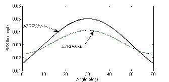
ripple characteristics it is found that the AZSPWM-II and AZSPWM-III will give the same ripple characteristics. Hence, in the proposed hybrid AZSPWM (HAZSPMW) algorithm AZSPWM-I and AZSPWM-III are considered. Based on the ripple characteristics, the zones of superior performance (which results in reduced ripple) can be found for each sequence. Then, the identified sequence will be applied to the VSI, so that the harmonic distortion can be reduced at all modulation indices.
Fig. 9 RMS stator flux ripple variation of AZSPW M algorithms at a supply frequency of 45 Hz
In the vector control algorithm, the induction motor operation is similar to a separately excited dc motor.
Fig. 10 Proposed HAZSPW M algorithms based indirect vector controlled induction motor drive
The reference d-axis and q-axis current signals, which are in synchronously rotating reference frame, are calculated by using the rotor flux and speed controller. Then, the error signals are generated by comparing these reference signals with the actual signals. The PI controllers will be fed with the error signals in order to calculate the voltage signals which are at synchronous speed. The transformation of voltages to the stator reference frame is done by using the rotor flux position and then converted into three-phase voltages. This process is carried out in 2-phase to 3-phase transformation block. The pulse pattern will be generated by using these 3-phase voltages. The HAZSPWM block will generate the switching pulses for the inverter as explained in the previous section.
To show the effectiveness of the proposed HAZSPWM algorithm, the simulation studies have been carried out on indirect vector controlled induction motor drive. For the simulation studies, the switching frequency is taken as 5 kHz and the dc link voltage is taken as 540 V. The specifications of the induction motor, which is used in this case study, are as follows:
4 kW, 400V, 1470 rpm, 4-pole, 50 Hz, Rs =1.57Ω, Rr =1.21Ω,
Ls =0.17H, Lr =0.17H, Lm =0.165 H and J = 0.089 Kg.m2.
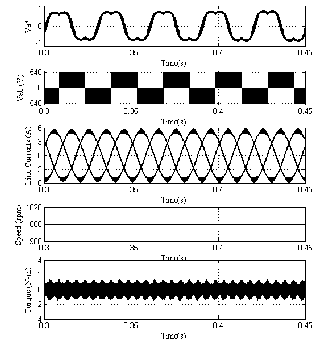
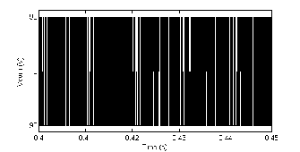
The steady state simulation results of SVPWM and proposed AZSPWM techniques based vector controlled induction motor drive are shown in from Fig. 11 to Fig. 22. From the simulation results of common mode voltage variations, it can be observed that the proposed AZSPWM algorithms give reduced CMV variations when compared with the SVPWM algorithm with slightly increased harmonic
IJSER © 2014 http://www.ijser.org
International Journal of Scientific & Engineering Research, Volume 5, Issue 6, June-2014 87
ISSN 2229-5518
distortion in the line currents due to the opposite pulses in the line voltages.
Fig. 11 steady state plots for SVPW M algorithm based vector controlled induction motor drive
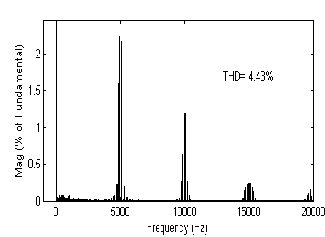
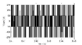
Fig. 12 Harmonic spectra of line current for SVPW M algorithm based vector controlled induction motor drive
Fig. 13 Common mode voltage variations for SVPW M algorithm based vector controlled induction motor drive
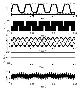
Fig. 14 steady state plots for AZSPW M1 algorithm based vector controlled induction motor drive
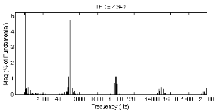
Fig. 15 Harmonic spectra of line current for AZSPW M1 algorithm based vector controlled induction motor drive
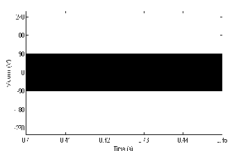
Fig. 16 Common mode voltage variations for AZSPW M1 algorithm based vector controlled induction motor drive
IJSER © 2014 http://www.ijser.org
International Journal of Scientific & Engineering Research, Volume 5, Issue 6, June-2014 88
ISSN 2229-5518
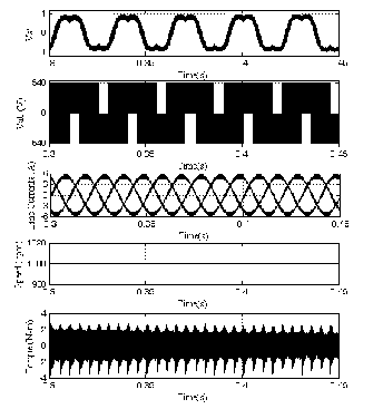
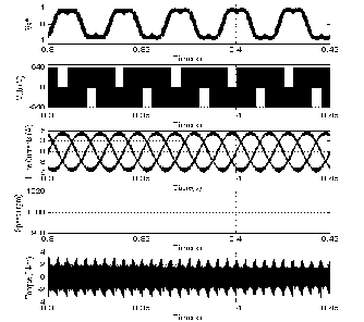
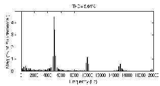
Fig. 17 steady state plots for AZSPW M2 algorithm based vector controlled induction motor drive
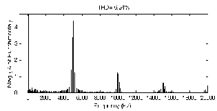
Fig.20 steady state plots for AZSPW M3 algorithm based vector controlled induction motor drive
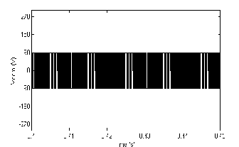
Fig. 18 Harmonic spectra of line current for AZSPW M2 algorithm based vector controlled induction motor drive

Fig.21 Harmonic spectra of line current for AZSPW M3 algorithm based vector controlled induction motor drive
Fig. 19 Common mode voltage variations for AZSPW M2 algorithm based vector controlled induction motor drive
Fig. 22 Common mode voltage variations for AZSPW M3 algorithm based vector controlled induction motor drive
To reduce the harmonic distortion at all modulation indices, a novel HAZSPWM technique is presented in this paper based on the concept of stator flux ripple. The simulation results of proposed HAZSPWM technique based FOC drive are shown in Fig. 23 – Fig. 25. From the simulation
IJSER © 2014 http://www.ijser.org
International Journal of Scientific & Engineering Research, Volume 5, Issue 6, June-2014 89
ISSN 2229-5518
results, it can be concluded that the proposed HAZSPWM technique gives reduced harmonic distortion when compared with the AZSPWM techniques.
VI. CONCLUSIONS
The classical space vector approach based AZSPWM techniques need the calculation of reference voltage vector, sector and angle calculations, which increases the complexity of the PWM technique. For reduced complications, a simple scalar approach has been presented in this paper. To evaluate the performance of the proposed approach based PWM algorithms, simulation studies have been carried out and results were presented. From the results it can be observed that the SVPWM algorithm gives large common mode voltage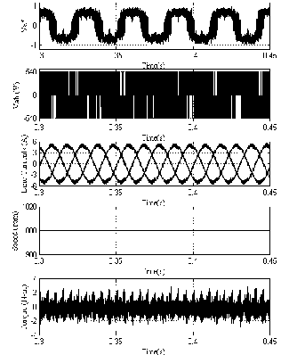
variations between
± Vdc
![]()
2 . But, the proposed AZSPWM
algorithms give reduced CMV variations between![]()
± Vdc 6 .
Moreover, it can be observed that the proposed AZSPWM algorithms give opposite pulses in the line to line voltages, which causes the increased harmonic distortion in the line current. Also, to reduce the harmonic distortion in the line current, a scalar based HAZSPWM technique is presented based on the concept of stator flux ripple. The performance is evaluated by using the simulation studies and results proved the effectiveness of the proposed HAZSPWM technique.
[1] Joachim Holtz, “Pulse width modulation – A survey” IEEE Trans.
Ind. Electron., vol. 39, no. 5, Dec 1992, pp 410-420.
Fig.23 steady state plots for proposed HAZSPW M algorithm based vector controlled induction motor drive
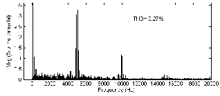
Fig.24 Harmonic spectra of line current for proposed HAZSPW M
algorithm based vector controlled induction motor drive
Fig. 25 Common mode voltage variations for proposed HAZSPW M
algorithm based vector controlled induction motor drive
[2] Heinz Willi Vander Broeck, Hnas-Christoph Skudelny and Georg Viktor Stanke, “Analysis and realization of a pulsewidth modulator based on voltage space vectors” IEEE Trans. Ind. Applicat., vol. 24, no. 1, Jan/Feb 1988, pp. 142-150.
[3] Ahmet M. Hava, Russel J. Kerkman and Thomas A. Lipo, “Simple analytical and graphical methods for carrier-based PWM-VSI drives” IEEE Trans. Power Electron., vol. 14, no. 1, Jan 1999, pp. 49-61.
[4] T.Brahmananda Reddy, J.Amarnath, D.Subbarayudu “Improvement of DTC Performance by Using Hybrid Space Vector Pulse Width Modulation Algorithm” International review of Electrical Engineering (I.R.E.E), vol. 2, no. 4, July/Aug 2007.
[5] Vladimir Blasko, “Analysis of a hybrid PWM based on modified space-vector and triangle-comparison methods” IEEE Trans. Ind. Applicat., vol. 33, no. 3, May/Jun 1997, pp. 756-764.
[6] S.Ogasawara and H.Akagi, “Modelling and damping of high frequency leakage currents in PWM inverter- fed Ac motor drive systems” IEEE Trans. Ind. Appl., Vol. 32, No.4, pp. 1105-1114, Sep/Oct, 1996.
[7] Erdman, J.M, Kerkman, R.J, Schlegel, D.W, and Skibinski, G.L, “Effect of PWM inverters on AC motors bearing currents and shaft voltages” IEEE Trans. Ind. Appl., Vol. 32, No.2, pp. 250-259, March/April, 1996.
[8] S. Ogasawara, H. Ayano, and H. Akagi, “An active circuit for cancellation of common-mode voltage generated by a PWM inverter,” IEEE Trans. Power Electron., vol. 13, no. 5, pp. 835–841, Sep.
1998.
[9] E. Ün, A.M. Hava “A near state PWM method with reduced switching frequency and reduced common mode voltage for three- phase voltage source inverters” IEEE-IEMDC Conf., pp. 235-240, May 2-5, 2007.
[10] A. M. Hava and E. Un, “Performance analysis of reduced common- mode voltage PWM methods and comparison with standard PWM
IJSER © 2014 http://www.ijser.org
International Journal of Scientific & Engineering Research, Volume 5, Issue 6, June-2014 90
ISSN 2229-5518
methods for three-phase voltage-source inverters,” IEEE Trans. Power Electron., vol. 24, no. 1, pp. 241–252, Jan. 2009.
[11] Ahmet M. Hava, N. Onur Cetin, A Generalized Scalar PWM Approach With Easy Implementation Features for Three- Phase,Three-Wire Voltage-Source Inverters” IEEE Trans on Power Electronics, Vol. 26, No. 5, May 2011, pp.1385-1395.
[12] Ahmet M. Hava, Emre Un, “A High-Performance PWM Algorithm for Common-Mode Voltage Reduction in Three-Phase Voltage Source Inverters” IEEE Trans on Power Electronics, Vol. 26, No. 7, July
2011, pp. 1988-2008.
[13] Chung-Chuan Hou, Chih-Chung Shih, Po-Tai Cheng, and Ahmet M.
Hava “Common-Mode Voltage Reduction Pulsewidth Modulation Techniques for Three-Phase Grid-Connected Converters” IEEE Trans on Power Electronics, Vol. 28, No. 4, April, 2013, pp 1971-1979.
IJSER © 2014 http://www.ijser.org
International Journal of Scientific & Engineering Research, Volume 5, Issue 6, June-2014 91
ISSN 2229-5518