International Journal of Scientific & Engineering Research, Volume 5, Issue 9, September-2014 589
ISSN 2229-5518
CMOS VLSI Design Technology and SRAM Design System
Assistant Prof. Yasmeen Saundatti
E&C Department, VTU University
Shaikh College of Engineering and Technology, Bhootramanhatti Belgaum -591156,
Karnataka, INDIA
yasmeen.s88@gmail.com
—————————— ——————————
Memory arrays often account for the majority of transistors in a CMOS system on chip. Random access memory is accessed with an address and has latency independent of the address. In contrast, serial access memories are accessed sequentially so no address is necessary. Random access memory is commonly classified as Read only Memory and Random access memory, they are also called as volatile and non volatile memory. Volatile memory retains its data as long as power is applied, while non volatile memory will hold data indefinitely. Like sequencing elements, the memory cells used in volatile memories can further be divided into static structures and dynamic structures. Static cells use some form of feedback to maintain their state, while dynamic cells use charge stored on a floating capacitor through an access transistor. Charge will leak away through the access transistor even while the transistor is off, so dynamic cells must be periodically read and rewritten to fresh their state. SRAM’s are faster and less troublesome, but require more area per bit than their dynamic counterparts DRAM’s.
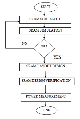
An SRAM Cell is the key component used to store binary information. A typical 6T SRAM cell uses two cross coupled inverters. Access transistors enable access to the cell during read operations and provide cell isolation during the not- accessed state. A 6T SRAM cell is designed to provide non destructive read access, write capability and data storage for as long as power supply is on. The flow chart for the design of low power SRAM read write system is as shown in figure 1. The steps involved in designing 6T SRAM cell are given below
6T SRAM Cell is simulated using microwind. The simulation is carried out to verify the correct functionality of the 6T SRAM Cell design. Write ‘1’ and write ‘0’ operation of the 6T SRAM Cell design is observed.
IJSER © 2014 http://www.ijser.org
International Journal of Scientific & Engineering Research, Volume 5, Issue 9, September-2014 590
ISSN 2229-5518
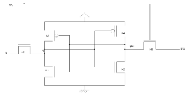
Figure2. 6T SRAM Cell
Figure 1: Flow chart for the design of low power SRAM read write system
It consists of pair of cross coupled inverters that use positive feedback to store value. Transistors M5 and M6 are 2 pass transistors that allow access to the storage nodes for reading and writing. To write a value into a SRAM cell the new value and its complement is driven on the bit lines and then the word line is raised. The new will overwrite the old value, since the bit lines are actively driven by write circuitry. To read a value from an SRAM the bit lines are pre charged high and the word line is raised turning on the pass transistors. Because one of the internal storage nodes is low, one of the bit lines starts discharging. A sense amplifier which is connected to the bit line senses which of the bit line is discharging and reads the stored value. The 6T SRAM cell is designed such that the pull up p-transistors are weakest, access transistors are of medium strength and pull-down nmos transistors are strongest to satisfy write and read constraints. The 6T SRAM cell is as shown in figure 2.
The basic SRAM block structure is as shown in figure 3. A row decoder gated by appropriate timing block signal decodes X row address bits and selects one of the word lines WL 0- WL N-1. The SRAM core consists of a number of arrays of NxM, where N is the number of rows and M is the number of bits. If an SRAM core is organized as a number of arrays in a page manner, an additional Z-decoder is needed to select the accessed page [1]. Figure 1 shows an example of SRAM with four pages of NxM arrays with the corresponding I/O blocks. SAM’s can be organized as bit- oriented or word oriented. In a bit oriented SRAM, each address accesses a single bit, whereas in a word oriented memory, each address addresses a word of n bits (where the popular values of n include 8, 16,
32, or 64). Column decoders or column MUXs (YMUXs) addressed by Y address bits allow sharing of a single sense amplifier among 2, 4 or more columns. The majority of modern SRAMs are self timed, i.e. all the internal timing is generated by the timing block within an SRAM instance. An additional chip select signal, introducing an extra decoding hierarchy level, is often provided in multi-SRAM chip architectures.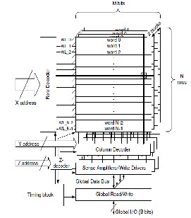
IJSER © 2014 http://www.ijser.org
International Journal of Scientific & Engineering Research, Volume 5, Issue 9, September-2014 591
ISSN 2229-5518
Fig. 3 SRAM block diagram
An SRAM cell proposed offers reduced gate and sub
threshold leakage currents and power in caches. In this paper an attempt is made to describe a CMOS VLSI design technology using SRAM as an example. The SRAM system can be developed using cadence, mentor graphics, microwind, ltspice software’s etc.The SRAM design design schematic layout can be drawn and verified.
For further optimization and better performance this
work can be carried out under lower CMOS technology such as 90nm, 45nm etc using different tools. And also much larger SRAM memory systems can be implemented.
1. CMOS VLSI Design- a Circuits and systems
perspective. Third edition-Neil H.E.WESTE, Macquarie university and the university of Adelaide , David HARRIS, Harvey Mudd College , Ayan Banerjee, Bengal Engineering and Science University.
2. Andrei Pavlov, Manoj Sachdev CMOS SRAM Circuit Design and Parametric Test in Nano-
Scaled Technologies. Process-Aware SRAM Design and Test.
3. Leakage power estimation in SRAM’S by Mahesh Mamidipaka, Kamal Khouri, Nikhil Dutt, Magdy Abadir. CECS Technical Report#03-32.Centre for Embedded Computer Systems, University of California, Irvine, CA 92697, USA
4. M.D.Powell, S.H.Yang, B.Falsafi etal… Gated- VDD: A circuit technique to reduce leakage in cache memories. In proceedings of International Symposium on Low Power Electronics and Design, July 2000.
5. Tutorial cadence design environment by Antonio
J.Lopez Martin.
6. S.Borkar.Design challenges of technology scaling.IEEE Micro, 19(4):23-29, august 1999.
7. T.Enomoto.Y.Oka and H.Shikano. self controllable voltage level (SVL) circuits, 38(7):1220-1226, july
2003.
8. Navid Azizi, Farid N.Najm.Andreas
Moshovos.Low leakage asymmetric cell
IJSER © 2014 http://www.ijser.org