International Journal of Scientific & Engineering Research, Volume 4, Issue 7, July-2013 1122
ISSN 2229-5518
Bandwidth Enhancement of Microstrip Patch Antenna Using Cavity Backing & Artificial Ground (AG) Structure
Manisha Dhindsa, Deepak Sood, C.C. Tripathi
Abstract— In this paper, a design of proximity coupled rectangular artificially grounded microstrip patch antenna has been proposed for the radar systems. The rectangular patches on multilayer structure have been rotated at 450 to increase the bandwidth. The antenna is fed by proximity coupled feed line on FR4 and Rogers multilayer substrates of dimension 47mm X 35mm. The proposed microstrip patch antenna with single patch fed by proximity feed line reported a bandwidth of 14%.By applying stacked patch configuration over it, two resonant modes are generated which enhanced
the bandwidth up to 40%. Moreover, in comparison, the proposed wideband microstrip patch antenna with artificial ground structure enhances the bandwidth up to 57.8%. By applying all these techniques, bandwidth improved by 9% as compare with the previous work. The parametric analysis has been done by varying the dimensions of the rectangular unit cells, gap between the unit cells and width of the proximity feed line using the HFSS ver. 11.
Index Terms— AG Structure, Cavity Backing, Feed Line, Microstrip Antenna, Multilayer structure, Proximity Coupled, Stacked Patch Configuration.
—————————— ——————————
1 INTRODUCTION
ANY modern communication systems require wide band microstrip antennas to achieve all requirements
like wide bandwidth (VSWR < 2) and high power efficiency. For many applications discussed in [1], [2], [3], [4], various microstrip patch antennas have been designed by using different techniques. Moreover, microstrip patch antennas are radiated using a feeding line, feeding can be done by different types e.g. sometimes feed line is given through directly connection with a patch like microstrip feed line and coaxial feed line [5], [6]. But to achieve some other requirements, feed line is not given directly to the radiating patch, this indirect connection of feed line is known as non-contacting feed line and its examples are proximity [7]-[11] and aperture coupled feed line [12],[13]. A Microstrip feed line and coaxial feed line has been used for the narrowband systems. The narrowband systems neither increase the capacity nor the power efficiency of the operating band during transmission. The proximity and aperture coupled feed line has been used especially for the wideband systems in which the feed line is not directly connected to the radiating patch [11]-[13].
————————————————
• Manisha Dhindsa is Assistant Professor in Department of Electronics & Communication at University Institute of Engineering & Technology, kurukshetra University, Kurukshetra, Haryana (India).
E-mail: manisha.dhindsa@yahoo.com
• Deepak Sood is Assistant Professor in Department of Electronics & Communication at University Institute of Engineering & Technology, kurukshetra University, Kurukshetra, Haryana (India). E-mail: deepaksood.uiet@gmail.com
• Chandra Charu Tripathi is Associate Professor in Department of Electronics & Communication at University Institute of Engineering & Technology, Kurukshetra University, Kurukshetra, Haryana(India).
This paper presents a design of microstrip patch antenna using a non-contacting feed line (proximity feed) and especially designed for C-Band applications. As reported in literature, proximity coupled feed line reported 13% maximum bandwidth as compare other feeding lines [14].
Till date, proximity coupled microstrip patch antenna had
reported a bandwidth of 21-22% [8], [11]. To enhance the
bandwidth, various techniques have been reported including [15] coplanar parasitic elements, stacked patch configuration [16], impedance matching network [17] and special shapes of radiating patches. A stacking of patches technique is preferred in antenna designs because it’s multiple layer structure sharing a common feed line and reduces the spurious back radiations. As mentioned in [6], antenna designed for L-Band using multilayer structure and bandwidth improved up to
25.7%. Hence, bandwidth depends upon the volume or
multilayer (stacked) structure, thickness and dielectric
constant of the substrate. The total height of the proposed wideband antenna is 6.7mm (0.6cm) which is mainly used for WLAN applications.
As discussed in literature [5], author presented broadband
artificial ground (AG) structure microstrip antenna designed
on the grounded plane using coaxial feed line and had reported 48.6% bandwidth. Now the same technique is applied in the proposed antenna design for enhancing the bandwidth. The structure of the paper is divided in following sections: Section II deals with the planar AGS structure. Section III illustrates the proposed antenna designs with its material description. Section IV discusses the parametric variations in AG dimensions and Section V offers some conclusions.
E-mail: tripathiuiet@gmail.com
IJSER © 2013
http://www.ijser.org
International Journal of Scientific & Engineering Research, Volume 4, Issue 7, July-2013 1123
ISSN 2229-5518
2 PLANAR AG STRUCTURE
Artificial magnetic conductor is a High Impedance Surface
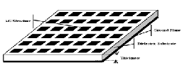
(HIS) which reflects the incident waves with 00 reflection phase and it is mainly divided into three categories: Photonic Bandgap Structure (PBG), Electromagnetic Band gap Structure (EBG) and Artificial Ground (AG) Structure. A planar AG structure is used as a reflector and made up of rectangular metal plates or unit cells along with air gaps between them as shown in fig. 1. An AG structure is mainly used for improving the bandwidth in microstrip patch antennas and the gap between these rectangular cells are plays very important role in bandwidth enhancement.
(a)

(b)
Fig.1. Layout of AG Structure (a) Artificial Ground Structure, (b) Unit Cell.
3 ANTENNA DESIGN
3.1 Proximity Coupled Cavity-Backed Microstrip Patch
Antenna
The geometry of the proposed antenna design-1 as shown in fig.2 with proximity coupled feed line. The dimensions of the rectangular patch are: 21.286mm X 17.4293mm, calculated by using design equations [14].
A proximity feed line is applied between the two different
dielectric substrates and the resonant mode shifts towards the
higher band of frequencies which illustrates that the antenna design-1 suffered with greater return losses at -7dB as shown in fig.3. To avoid these losses, a circular cavity has been etched on the grounded substrate with radius of 13.7557mm and achieved -10dB bandwidth up to 14% (4.2 to 4.8) GHz. As conclusion from fig. 3, without using any circular cavity in antenna design, the antenna has been suffered with maximum return losses at 4.8GHz frequency. By etching a circular cavity in the grounded substrate, the return losses are to be reduced up to -47dB and antenna resonates at exactly 4.5GHz resonant frequency.
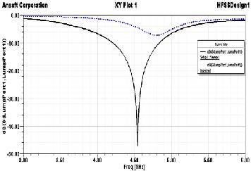
Fig.3. Simulated Results of simple proximity coupled MPA (dash line) and with circular cavity backing
3.2 Stacked Microstrip Patch Antenna
To enhance the bandwidth, a stacked patch technique has been applied over the antenna design-1. It means that one more substrate layer along with patch is applied over the antenna design whose dimensions are same as previous one calculated by using design equations [14].
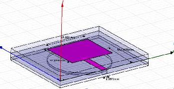
Fig.2. Antenna Design-1 with Proximity Feed Line
IJSER © 2013 http://www.ijser.org
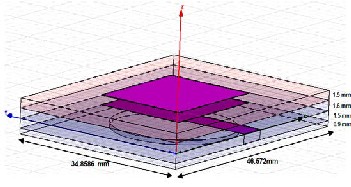
Fig.4. Antenna Design-2 Stacked Configuration
International Journal of Scientific & Engineering Research, Volume 4, Issue 7, July-2013 1124
ISSN 2229-5518
In fig. 4, antenna design-2 showing a multilayer structure
which shows that the stacked patches sharing a common feed line and its impedance matching, mutual coupling can be achieved with the help of circular cavity. By using a stacked patch technique, two resonant modes are generated which enhance the impedance bandwidth up to 40% (3.5 to 5.3) GHz as shown in fig.5. By using a single patch with proximity feed line and achieved bandwidth is 14%. While using stacked patches (double patches) over the antenna design, two resonant modes are produced. The first resonant mode increases with return losses of -34dB and second resonant mode decreases with return loss of -18dB.
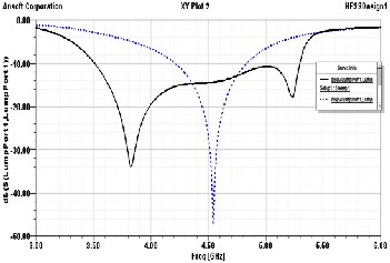
Fig.5.Simulated Results for single patch MPA (dash-dotted line) and stacked patch configuration (solid line)
3.3 Artificial Ground (AG) Structure
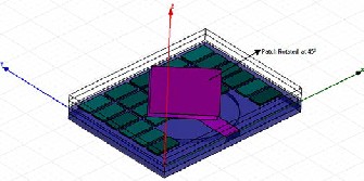
An artificial ground structure illustrates a periodic structure of rectangular unit cells which are placed on the feed substrate in proposed antenna design-3 as shown in fig.6. The dimensions of the unit cells are 7.7346mm X 3.9292mm. In this proposed antenna design-3, both stacked patches have given a rotation of 450 in anticlockwise direction and impedance bandwidth improved up to 57% (3.27 to 6.03) GHz as shown in fig.7.
(a) Top view
(b) Side view
Fig.6. Antenna Design-3 with AG Structure, (a) Top view, (b)
side view
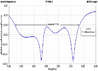
Fig.7.Simulated S11 parameter for AG Structure Antenna
The description of the design parameters used in the proposed antenna designs are shown in table 1.
TABLE 1
PARAMETERS FOR THE PROPOSED ANTENNA
Parameter | Value (mm) |
Substrate-1 thickness | 1.5 |
Substrate-2 thickness | 1.6 |
Rectangular plate thickness | 0.5 |
Ground Substrate thickness | 1.5 |
Feed width | 4.8673 |
Feed length | 15.13175 |
Cavity radius | 13.7557 |
Cavity depth | 0.9 |
4 SIMULATED RESULTS
4.1 Variation in Rectangular Plate Width of AG
structure
IJSER © 2013 http://www.ijser.org
International Journal of Scientific & Engineering Research, Volume 4, Issue 7, July-2013 1125
ISSN 2229-5518
In AG structure, varying the width of the rectangular unit cells and studying its effect on bandwidth as discuss or given in Table 2. When the width of the cell is 7.7346mm, then the two resonant modes are to be produced with a great reduction in return losses. This width also affected the bandwidth and makes the operating band wider (57.8%). By using rectangular unit cell width is 8.7346mm in AG structure; both the resonant modes are decreased.
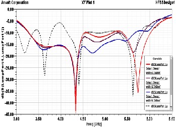
Fig.8. Simulated S11 for the AG structure antenna for different values of the width of the rectangular cell
If the unit cell width is 9.7346mm, only one resonant mode exists with return loss of -34dB and its gives the band of frequencies (3.27-5.69) GHz reported a bandwidth of 54%. As conclusion, as the width of the unit cell increases more in artificial ground structure then the bandwidth decreased and there is production of so many resonating modes as shown in fig.8.
TABLE 2
VARIATION OF WIDTH OF THE UNIT CELL
4.2 Variation in gap between the unit cells of AG
structure
In AG structure, the gap is 3mm between the unit cells where the first resonant mode exists with return losses of -44dB and second resonant mode exists with return loss of -35dB as shown in fig.9. But this gap doesn`t gives a desirable -10dB bandwidth. So, the gap becomes decreases up to 2mm, but there is no effect on impedance bandwidth except reduction of the second resonant mode. By taking the gap between the cells is 1mm, in which bandwidth is measured with the help of two resonant frequencies are 3.2242 and 5.8483 GHz, reported
-10dB bandwidth up to 57.8%.
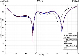
Fig.9. Simulated S11 parameters for different values of Gap present between the rectangular cells (3mm, 2mm, 1mm)
4.3 Effect of feed width on performance
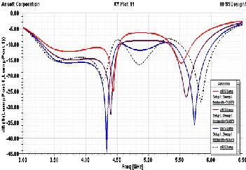
As the feed width decreases with 2.8673mm, then the operating band get suppressed without any existence of -10dB bandwidth.
Fig.10. Variation of Feed Width versus Frequency
IJSER © 2013 http://www.ijser.org
International Journal of Scientific & Engineering Research, Volume 4, Issue 7, July-2013 1126
ISSN 2229-5518
By taking the feed width of 3.8673mm, the losses are to be reduced up to -32dB (first resonant mode) and -26dB (second
resonant mode). When the feed width increases with value
5.8673mm, then the three resonant modes are generated, this
makes band wider as shown in fig. 10. So the value of the feed width should be taken more than 3.8673mm but less than
5.8673mm. When the bandwidth increases then side lobes in
the radiation pattern decreased as shown in fig. 11(a). This radiation pattern illustrates that by using the bandwidth enhancement techniques, back lobes are totally reduced. The major lobe becomes increases more widely and gives a directional radiation pattern as shown in fig. 11(b).
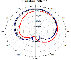
Fig.11. (a) Radiation Pattern for Phi= 00
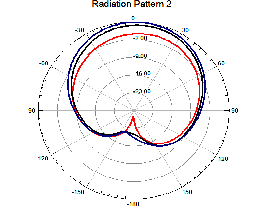
Fig.11. (b) Radiation Pattern for Phi= 900
5 DISCUSSION
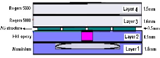
A Multilayer structure having four layers, in which layer3 patch and layer4 patch has been rotated at 450 to enhance the bandwidth as shown in fig. 6. A feed line is given on layer2 and the bottom grounded substrate behaves as a layer1. Beneath the layer4 & layer3, a periodic structure is placed in the form of rectangular cells. This periodic structure is known as AG (artificially ground) structure which reflects the
incident wave with 00 reflection phase. This same technique was studied in paper [5]. In work [5], artificial ground
structure fed by coaxial fed line had demonstrated a great enhancement of impedance bandwidth (48.6%). The antenna size was: 40mm X 39mm, fabricated on substrate material (Rogers 5880) having 6 X 4 unit cells in AG structure.
Our proposed antenna design results are better than the
design [5] given by Nakamura [5] due to following reasons:
1. The proposed design size is almost same as the design specified in [5]. But in proposed AG structure in fig6, the number of unit cells (6 X 5 unit cells) are increased along X and Y axis in symmetrical manner.
2. A multilayer antenna is designed using a high
dielectric substrate materials e.g. Rogers Duroid 5880
(Єr=2.2), and Fr4 epoxy (Єr=4.4).
3. A proximity feed line is used in multilayer design as
it provides wider bandwidth as compare to other feeding techniques. To enhance the mutual coupling between patch and the proximity feed line, a circular cavity has been etched in the grounded substrate.
6 CONCLUSION
In this paper, bandwidth enhancement has been done using multilayer structure; proximity coupled feed line, cavity backing and AG structure. A wideband microstrip patch antenna is designed for C-Band (3-8GHz) Radar applications. The study has shown that the cavity backing reduce the surface waves in the substrate and maintained a strong mutual coupling between the multilayer substrates. A multilayer structural antenna has been designed and simulated, achieved two resonant modes with -10dB bandwidth of 40%. The bandwidth enhanced up to 57.8% using a periodic AG structure with overall size of 47 X 35 mm2 radiated at resonant frequency of 4.5 GHz with acceptable radiation efficiency.
REFERENCES
[1] Hsien-Wen Liu, Chung-Hsun Weng and Chang-Fa Yang, “Design of near-field edge-shorted slot microstrip antenna for RFID handheld reader applications,” IEEE Antennas and Wireless Propagation Letters, vol.10, pp. 1135-1138, 2011.
[2] Jean-Christophe Diot, Teihoarii Tarati, Baptiste Cadilhon, Bruno Cassany, Patrick Modin and Eric Merle, “Wideband patch antenna for HPM applications,” IEEE Transactions on plasma science, vol.39, no.6, pp. 1446-1454, June 2011.
[3] C. F. Tseng, S.C. Lu, and Y. C. Hsu, “Design of microstrip antenna with modified annular-ring slot for GPS application,” PIERS proceedings, pp. 242-245, September, 2011.
IJSER © 2013 http://www.ijser.org
International Journal of Scientific & Engineering Research, Volume 4, Issue 7, July-2013 1127
ISSN 2229-5518
[4] Wen-Cheng Tzou, Hua-Ming Chen, Ying-Chung Chen and Cheng-Fu Yang, “Bandwidth enhancement of U-slot patch antenna on high permittivity ceramic substrate for Bluetooth application,” Microwave and Optical Technology Letters, vol.36, no.6, pp. 499-501, March, 2003.
[5] Teruhisa Nakamura and Takeshi Fukusako, “Broadband design of circularly polarized microstrip patch antenna using artificial ground structure with rectangular unit cells,” IEEE Transactions on Antennas and Propagation, vol.59, no.6, pp. 2103-2110, June
2011.
[6] Luiz C. Trintinalia, “Simple excitation model for coaxial driven monopole antennas,” IEEE Transactions on Antennas and Propagation, vol.58, no.6, pp 1907-1912, June 2010.
[7] Yong-Xin Guo, Chi-Lun Mak, Kwai-Man Luk and Kai-Fong Lee, “ Analysis and design of L-probe proximity fed patch antennas,” IEEE Transactions on Antennas and Propagation, vol.
49, no.2, pp. 145-149, February 2001.
[8] Steven Gao and Alistair Sambell, “Dual-polarized broad-band microstrip antennas fed by proximity coupling,” IEEE Transactions on Antennas and Propagation, vol.53, no.1, pp. 526-
530, January 2005.
[9] Luis Inclan-Sanchez, Jose-Luis Vazquez-Roy and Eva Rajo- Iglesias, “Proximity coupled microstrip patch antenna with reduced harmonic radiation,” IEEE Transactions on Antennas and Propagation, vol.57, no.1, pp. 27-32, Jan. 2009.
[10] Ee Lee, Kin Meng Chan, Peter Gardner and Terence E.
Dodgson, “Active Integrated Antenna Design Using a Contact- Less, Proximity Coupled, Differentially Fed Technique,” IEEE Transactions on Antennas and Propagation, vol. 55, no.2, pp. 267-
276, February 2007.
[11] Shi-Wei Qu and Quan Xue, “A Y-Shaped Stub Proximity Coupled V-Slot Microstrip Patch Antenna,” IEEE Antennas and Wireless Propagation Letters, vol. 6, pp. 40-42, 2007.
[12] Sumanth Kumar Pavuluri, Changhai Wang and Alan J.
Sangster, “High efficiency wideband aperture-coupled stacked patch antennas assembled using millimeter thick micromachined polymer structures,” IEEE Transactions on Antennas and Propagation, vol.58, no.11, pp. 3616-3620, Nov.
2010.
[13] Christopher J. Meagher and Satish Kumar Sharma, “A wideband aperture-coupled microstrip patch antenna employing spaced dielectric cover for enhanced gain performance,” IEEE Transactions on Antennas and Propagation, vol. 58, no.9, pp. 2802-2810, September 2010.
[14] R Garg, P. Bhartia, I. Bahl, and A. Ittipiboon, “Microstrip
Antenna Design Handbook,” Norwood, MA: Artech House,
2001.
[15] C.K. Wu and K.L.Wong, “Broadband microstrip antenna with directly coupled and gap-coupled parasitic patches,” Microw. Opt. Technol. Lett., vol. 22, pp. 348-349, September 1999.
[16] Zhang-Fa Liu, Pang-Shyan Kooi, Le-Wei Li, Mook-Seng Leong and Tat-Soon Yeo, “A method for designing broadband microstrip antennas in multilayered planar structures,” IEEE Transactions on Antennas and Propagation, vol.47, no.9, pp 1416-
1420, September 1999.
[17] H.F. Pues and A.R. Van de Capelle, “An impedance matching technique for increasing the bandwidth on microstrip antennas,” IEEE Transactions on Antennas and Propagation, vol. AP-37, no. 11, pp. 1345-1354, Nov.,1989.
IJSER © 2013 http://www.ijser.org