International Journal of Scientific & Engineering Research, Volume 1, Issue 3, December-2010 1
ISSN 2229-5518
An FPGA Based Digital Controller for AC Loads Utilizing Half and Full Wave Cycle Control
Shaiyek Md. Buland Taslim, Shaikh Md. Rubayiat Tousif
Abstract— Voltage control for AC loads can be performed by controlling phase and cycles of AC voltages reaching load end. Cycle control tends to be more beneficial, as it reduces the amount of harmonic frequency in the circuit compared to phase control circuit. W hen a wave is passed in cycle control circuit, then either an entire half cycle or a complete full cycle is passed, hence eliminating the sharp change in the wave which is typical in phase control, causing harmonic frequency in the circuit. Cycle control is the most convenient process to control the output voltage for reducing RFI and this is the very approach that has been utilized in designing this project. This project utilized a voltage comparator to generate a digitized AC voltage and an SCR (Silicon Controlled Rectifier) to supply the required AC cycles to the load. The central controller was a digital controller, implemented in a Xilinx Spartan - 2 FPGA. The digital controller utilized a Finite State Machine (FSM) that took in digital AC signal and the desired percentage of load voltage. W ith this information it passed a certain number of half or full cycles to the load, at the same time ensuring that, number of these AC cycles satisfied users percentage requirement. The digital controller was modeled in VHDL (Hardware Description Language), synthesized with XST tool, placed and routed in a Xilinx Spartan- 2
FPGA (xc2S50 – pq208) in Xilinx ISE 9.1i WebPack design environment. The placed and routed designed was implemented in the Pegasus FPGA board from Digilent containing the above mentioned FPGA. The simulations and the outputs of the implemented hardware accorded with the expected outputs.
Index Terms— Cycle control, Finite State Machine (FSM), RFI, simulations, VHDL
—————————— • ——————————
1 INTRODUCTION
HIS project models and implements a Voltage Con- troller by employing AC cycle control. The basic idea behind the project was to control the amount of cycles reaching the load. By controlling the cycles the amount of voltage generated at the load end was controlled. This project was designed in order to fulfil the following objec-
tives:
To develop a device that takes in user input (in percen- tage) and gives an equivalent corresponding output power to an AC load but by randomly controlling the cycles that are forwarded to the load.
To control the voltage of an AC load using both half and full wave AC cycle control method.To eliminate DC com- ponent completely from the desired output.To sample DAC in a manner this avoids noise during state transition. To enable the user to select multiple clock frequencies.
To continuously monitor the percentage of half and full cycles being applied to the load and whether they meet the users’ requirements.
To model the central digital controller in VHDL, synthes- ize the logic in XST and place and route it in a Spartan – 2 (xc2s50-pq208) FPGA in Xilinx ISE WebPack 6.3i design environment and implement it in the above mentioned FPGA.
2. CONTROL Cycle
In this process the cycles of the AC wave that reaches the load end is controlled. It can be controlled using half cycle and full cycle wave control. This also works by using any form of thyristor switches to pass a predetermined half or full cycle of an AC wave. The cycles can be passed in a certain order or randomly both achieving similar re- sult. Fig 1 gives a brief idea about cycle control. According to the figure the output receives roughly 50% power. When the gate pulses are given accordingly to the thyris- tor switch, and then in case of half wave control half of the cycle passes to the output. Whereas for full wave control once the gate of the thyristor switch receives gate pulse it allows an entire cycle to pass to the output. In this way the motor receives varying pulses to drive it on and off thus allowing control over the speed of the motor.
This project employs cycle control method in order to control the amount of AC Voltage reaching the load, spe- cifically motor and thus controlling its speed. This method was chosen due to the following advantages over the other mentioned methods.
Phase control tends to clip off a certain portion of the input wave in order to reduce the power reaching the out- put. This clipping causes a sharp change in voltage level
IJSER © 2010 http://www.ijser.org
International Journal of Scientific & Engineering Research, Volume 1, Issue 3, December-2010 2
ISSN 2229-5518
which when analyzed in the frequency spectrum gives rise to a lot of harmonic frequencies thus causing a lot of RFI (Radio Frequency Interference). This problem is not faced in cycle control as when a wave is passed then either an entire half cycle or a full cycle is passed thereby eliminat- ing the sharp change in the wave which gives rise to RFI in the first place.
The cycle control is similar to the PWM method in DC control; just in the case of DC the voltage level switches between two extremes whereas in this process the voltage rises gradually from 0 to a high and then eventually comes back to 0.
Blending randomness along with cycle control also tends to make the results better
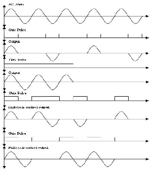
Fig. 1 Cycle Control
2.1 Controller Designed For This Project
. Due to reasons described above, cycle control was chosen for this project. This controller can control both half and full wave. It has the capability to reduce DC component from the output. It can continuously monitor whether the percentage of the half cycle matches with the desired percentage of half cycle. In this project several different bits and seed have been tried and observed as shown in chapter 4, and only the best result was used, which ensured the maximum possible ran- domness in the output and least deviation from desired per- centage of half or full cycles. It sampled DAC_in (the digi- tized AC signal that is necessary to be fed to the controller in order to identify the zero crossings) all the time, thereby in- creasing the risk of accidental state transition of the controller due to the noise in DAC_in, especially during its HIGH to LOW or LOW to HIGH transition.
2.2 VHDL and fpga usage
VHDL (Very high speed integrated circuits Hardware Description Language) was used in order to model and implement the digital controller used in this. The advan- tages of using VHDL over conventional methods are stated below
If basic combination of IC’s were to be used then verify- ing it would become really hard. The design would be really large with extensive amount of wiring making it nearly impossible to debug any errors if it existed within the device. This problem is fixed when VHDL is used, as using VHDL the entire device can be modeled and then functionally checked to verify if the device would operate properly before actually implementing the device onto a digital controller. After functional verification the VHDL description was synthesized and placed and routed in a Spartan – 2 FPGA. After verifying post route simulation, it was implemented in that FPGA. The advantage of FPGA over ASICs is that one can easily implement the design without the need for fabrication. In addition unlike ASICs, FPGAs can be reprogrammed, so design upgrade is much easier in an FPGA.
Different bits and combinations of random numbers give different results. Some give slightly better precision on desired speed input whereas other combinations give very low precision on the speed. To find out which com- bination gives the best output results would be nearly im- possible if it were to be done manually using various IC combinations but with VHDL the device can be repro- grammed over and over again and then the output results simulated and then analyzed to see which combination gives the best results on the desired speed.
There are other factors such as the clock speed, seed of the random number generator etc… which improves the precision of the desired speed but again finding the op- timal combination is nearly impossible if it were designed using basic ICs or ASICs, but in VHDL all these factors can be varied one by one and their output simulations checked and then eventually the optimized algorithm can be pro- grammed on to the controller.
3. EXPERIMENTAL DETAILS
3.1 Randomness
Randomness is a very integral part of the digital con- troller of this project. Randomness in the controller output allows reducing RFI considerably more than it would re- duce without its inclusion. The inclusion of randomness allows for the device to generate gate pulse signals with- out any specific sequence thus making the switching fea- ture unpredictable.
3.2 Pseudo-Random Number Generator
In order to understand pseudo random number genera- tor it is first necessary to understand what a Linear Feed- back Shift Register (LFSR) is. It is a sequential shift register
IJSER © 2010 http://www.ijser.org
International Journal of Scientific & Engineering Research, Volume 1, Issue 3, December-2010 3
ISSN 2229-5518
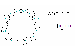
with combinational feedback logic around it that causes it to pseudo randomly cycle through a sequence of binary values. LFSRs often have both area and speed advantages over a functionally equivalent design that doesn’t use LFSR’s. Its typical applications include Pseudo-random number generators, Built in self test (BIST), data encryp- tion and decryption, data integrity checksum, and data compression techniques. Operation of LFSRs typically depends on its feedback capability. This feedback around a LFSR’s shift register comes from a selection of points (taps) in the register chain and constitutes either XORing or XNORing these taps to provide tap(s) back into the reg- ister. Register bits that do not require an input tap oper- ates as a shift register. Fig.2 shows a typical LFSR, the XOR gate provides feedback to the register that shifts bits from left to right. The maximal sequence 2n - 1, where n is the number of bits in the number, consists of every possible state except the "0000" state. It is this feedback that allows the LFSR to loop through repetitive sequences of pseudo- random values. The choice of taps determines how many values there are in a given sequence before the sequence is repeated.
A pseudo random number generator is an algorithm that is used for generating a sequence of numbers that approximately generates a random number sequence. The sequence is not truly random but it often appears to lack any definite pattern, any pseudo random number genera- tor with a finite internal state will repeat after a very long sequence of numbers. A pseudo random number genera- tor can be started from an arbitrary starting state, using a seed state other than 0. It will always produce the same sequence thereafter when initialized with that state. For instance if bit 0 and bit 2 of a 3 bit register are taps for ge- nerating pseudo random number then it will give a se- quence of maximum length of 23 – 1 = 8 – 1 = 7. Thus it will sequence through every possible value, except where all three bits are at logic 0, before returning to its initial value. For any given number of bits there may be many tap combinations which give maximal length sequence. For example a 10 bit number has two combinations of taps which give maximal length sequence (2, 9 and 6, 9). The sequence in which the binary values will be generated depends on which tap combination is chosen.
Fig.2: A typical 4-bit LtFSR with its state diagram.
3.3 Operation
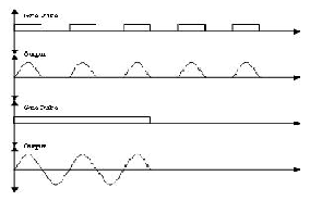
If randomness was not utilized into the design then in order to obtain 50% power the output would have to be either switched on and off periodically or kept on for half the time and then off for the remaining time as shown in Fig.3. As the figure demonstrates for non random gate pulses, the gate pulses would have to be either switching at every positive cycle or negative cycle or would have to be HIGH constantly up to half of the time for which the motor is to be on. The latter method is much less feasible as the motor may not always run for a concise period of time, thus the time for which the motor should be on be- comes unpredictable. When the pulses are generated in regular intervals then for shorter gaps there is a risk of the AC signal being interpreted by the motor as a DC signal (i.e. consecutive positive cycles or negative cycles on the output gives rise to DC component even for AC inputs). Thus the motor sees the average value of the input as a DC input.
IJSER © 2010 http://www.ijser.org
Fig.3: Output Waveforms for Non Random Gate Pulses
International Journal of Scientific & Engineering Research, Volume 1, Issue 3, December-2010 4
ISSN 2229-5518
On the other hand when randomness was included this problem was almost overcome. One possible scenario in random outputs could be two consecutive positive cycles or two consecutive negative cycles. This again would give rise to DC component which is not desired hence a me- chanism was devised, which will be collaborated on in the later chapters, to overcome this problem thus generating a true AC signal as an input to the load. The gate pulses were triggered at random sequences thus the motor was not getting a constant average value nor was it switched on or off for a prolonged period of time. Again since there are no consecutive positive cycles or negative cycles hence there is no risk of getting a DC signal thus when analyzed in the frequency spectrum the RFI generated tends to be considerably less.
3.4 Results for Application of Randomness and its
Analysis
The pseudo random number generator was used in col- laboration with a comparator in order to generate the out- put pulses that would allow for the switching of the AC signal. The pulses generated by the device, after being subjected to different seeds and also different bit pseudo random number sequence, have been used to simulate the outputs and their results tabulated.
The simulations were done for both half cycle operation and also full cycle operation. Though different number of bits of pseudo random number generator was designed, only the results for 5 bit are shown since this was the de- sign which was synthesized and placed and routed onto the FPGA. The criteria that were analyzed were the effects of applying different seeds, different clock frequencies, different speed requirement and finally different number of bits.
The simulation results prove that the value of the seed that is given to the pseudo random number generator plays an important part in maintaining the accuracy of the output. No finite conclusions could be made from the re- sults stated above thus certain partial deductions were made. An important observation which was made was that full wave control yields better individual results than half wave control which was as expected. Low value seeds allowed yielding most precise results, then mid value seed and lastly high value seed. Usually a higher clock should give more randomness and thus should activate Mo- tor_Out signal more randomly at the same time maintain- ing desired speed. But this was not the case, it was seen that the percentage deviation from the required speed was less in 5 KHz clock i.e. slow clock frequency, than it was in fast clock frequency for majority of the cases. After this it is now necessary to implement the algorithm of the device onto a digital controller but in order to do that the various components (registers, comparators, random number ge- nerators etc… all of which function on receiving control signals) of the device must be modeled.
For 5 bit random number sequence:
When 5 bits for generating random number was used then the following results were obtained.
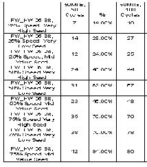
TABLE 1
HALF WAVE OPERATION FOR 50MHZ CLOCK FREQUENCY
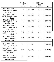
The best results obtained for 25% was when very high value seed was used, for 50% was when mid value seed was used and for 75% was when very low value seed was used.
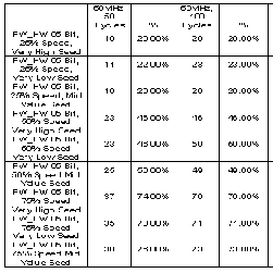
TABLE 2
FULL WAVE OPERATION FOR 50MHZ CLOCK FREQUENCY
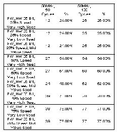
The best results obtained for 25% was when mid value seed was used, for
50% was when mid value seed was used and for 75% was when very low
value seed was used.
IJSER © 2010 http://www.ijser.org
International Journal of Scientific & Engineering Research, Volume 1, Issue 3, December-2010 5
ISSN 2229-5518
TABLE 3
HALF WAVE OPERATION FOR 5 KHZ CLOCK FREQUENCY.
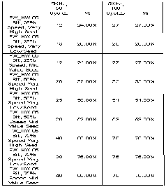
The best results obtained for 25% was when both very high and low value seed was used, for 50% was when very low value seed was used and for 75% was when very low value seed was used.
TABLE 4
FULL WAVE OPERATION FOR 5 KHZ CLOCK FREQUENCY
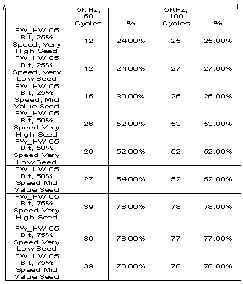
The best results obtained for 25% was when very high value seed was used, for 50% was when very high value seed was used and for 75% was when very low value seed was used.
For 32 bit random number sequence:
When 15 bits for generating random number was used then the following results were obtained.
TABLE 5
HALF WAVE OPERATION FOR 50 MHZ CLOCK FREQUENCY
The best results obtained for 25% was when very low value seed was used, for 50% was when mid value seed was used and for 75% was when very low value seed was used.
TABLE 6
FULL WAVE OPERATION FOR 50 MHZ CLOCK FREQUENCY
The best results obtained for 25% was when mid value seed was used for
50% was when mid value seed was used and for 75% was when very high
value seed was used.
The preceding simulation results prove that the value of the seed that is given to the pseudo random number generator plays an important part in maintaining the accu- racy of the output. No finite conclusions could be made from the results stated above thus certain partial deduc- tions were made. An important observation which was made was that full wave control yields better individual results than half wave control which was as expected. Low value seeds allowed yielding most precise results, then mid value seed and lastly high value seed. Usually a high- er clock should give more randomness and thus should activate Motor_Out signal more randomly at the same
IJSER © 2010 http://www.ijser.org
International Journal of Scientific & Engineering Research, Volume 1, Issue 3, December-2010 6
ISSN 2229-5518
time maintaining desired speed. But this was not the case, it was seen that the percentage deviation from the re- quired speed was less in 5 KHz clock i.e. slow clock fre- quency, than it was in fast clock frequency for majority of the cases. After this it is now necessary to implement the algorithm of the device onto a digital controller but in or- der to do that the various components (registers, compara- tors, random number generators etc… all of which func- tion on receiving control signals) of the device must be modeled.
4 DATAPATH
A datapath is a collection of functional units, such as ALU’s or multipliers that perform data processing opera- tions. Most digital systems consist of a datapath and a con- trol unit. In this project the control unit is the FSM that sends various control signals to the Datapath to control the components residing within it. This project contains lots of typical components like registers, counters, comparators, etc…
5 FSM DESIGN
The FSM as stated above is divided in to two parts the PSR and the NSOL.
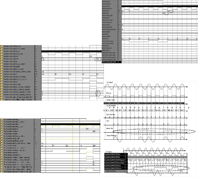
Fig. 6: Functional simulation 3
Fig.7: Functional simulation 4
Fig. 4: Functional simulation 1
Fig. 5: Functional simulation 2
Fig. 8: Theoretical and functional simulation of outputs
IJSER © 2010 http://www.ijser.org
International Journal of Scientific & Engineering Research, Volume 1, Issue 3, December-2010 7
ISSN 2229-5518
Thus after comparing the above two figures it can be seen that the practical and the theoretical outputs match exactly. Out of 20 half cycles only 9 are passed to the out- put therefore giving nearly 50% power to the load. Thus it is evident from this that the device is functioning as ex- pected.
6. LOGIC SYNTHESIS, AUTOMATIC PLACE-AND- ROUTE, POST-ROUTE SIMULATION AND IMPLEMENTATION
In order to implement a HDL design, logic synthesis has to be done. This step is taken after the design algo- rithm has been rectified and its functionality verified using functional simulations. The device for this project was syn- thesized using Xilinx Synthesis Tool (XST) inside Xilinx ISE WebPack 6.3i design environment. After synthesis the device was placed and routed in a Spartan 2 FPGA (xc2s50-pq208). The post route verification was performed through ModelSim XE ||| 6.2c.
7. SUGGESTION FOR FUTURE WORK
Some of the future work associated with this project can include doing the necessary hardware modifications. A better quality of SCR could be used, which will ensure the safety of the loads. It will also remove the distortion from the output. A better comparator will provide with proper DAC_in with no noise and error. It will also allow us to use fast clock. A FPGA with more input and output switches and pins will allow testing of the controller with larger pseudo-random number generators.
If all these needs could be fulfilled then the device could extensively used to reduce Radio Frequency Interfe- rence as this system has the potential to diminish RFI to almost zero.
8. CONCLUSIONS
This project implements a digital controller for AC loads that utilizes both half and full wave control. The user can select which type of control the controller should select. It has removed many limitations of a previous project. The upgraded features (other than the ability to implement both half and full wave control) includes eli- minating DC component from the output in half wave control, sampling digitized AC (DAC_in) in a manner that avoids noise during HIGH to LOW or LOW to HIGH tran- sition, an analysis of which pseudo-random number gene- rator gives best possible output and continuous monitor- ing of whether the output is meeting the users require- ments (whether the percentage of half or full cycles ap- plied to load is close to the desired percentage). The digital controller was implemented in Spartan -2 FPGA, with its operation verified through functional and post fit simula- tion as well as through CRT (cathode ray tube) oscillos- cope. The operation of voltage comparator and SCR was also verified through CRT oscilloscope.
As the objectives of the project were successfully met, further improvement of this project can be a project or research topic for future students.
ACKNOWLEDGMENT
We would like to thank our teacher and supervisor for this project Mr. Shahriar Masud Rizvi. We would also like to thank our other group members for their support and co operation.
REFERENCES
[1] Shahriyar Masud Rizvi, “A Half Wave Controller for AC Loads”, Senior Design
[2] Project, Department of Electrical and Computer Engineering, University of Wyoming, USA, 2000.
[3] Douglas J. Smith,“VHDL Chip Design – A Practical Guide for
Desiging
[4] Robert F Coughlin, Frederic F Driscoll, “Operation Amplifiers and
Linear Integrated
IJSER © 2010 http://www.ijser.org
International Journal of Scientific & Engineering Research, Volume 1, Issue 3, December-2010 8
ISSN 2229-5518
IJSER <S>2010 http/lwww l!ser org