
Inte rnatio nal Jo urnal o f Sc ie ntific & Eng inee ring Re se arc h Vo lume 3, Issue 1, January -2012 1
ISS N 2229-5518
An Automatic Voice-Controlled Audio Amplifier
Jonathan A. Enokela and Jonathan U. Agber
Abs trac t— The delivery of the proper quality of audio signals to the audience in the entertainment, public and other environments is of great, and sometimes critical, importance. This alw ays requires that the audio signals be of the correct intensity to the hearing of the audience, especially if the signals come f rom diff erent sources. This w ork presents a system w hich automatically f ades out the main stream signal w hen signals f rom other sources are received. By arranging the circuit such that the signal f rom the other sources continuously drives a pair of bipolar junction transistors tow ards heavier saturation, the mainstream signal w as attenuated by as much as 3 dB.
Inde x Terms— Audio Amplif ier, Electronic Control, Attenuation, Voice Control, Public Address System, Audio Fading.
—————————— ——————————
N many instances in public addressing environment, radio stations, television houses and in other places, the need for two signals to be simultaneously sent to the listeners arises. In almost all cases the audio signals will have to operate in such a way that one source is attenuated while the other is amplified for the listeners to have their attention drawn to the one that is amplified momentarily. In a radio house, for instance, the announcer might want to put out an urgent message to the listeners while the music that he has been playing at the background will be attenuated. Most existing facilities require that the announcer use his hand to control the volume of the music being played at the background while he makes his announcements. This process has some drawbacks: in the first place, the degree of attenuation that the announcer imposes on the amplifier is highly subjective. This results in the background music being either too loud or too faint.
Secondly, a manual control will wear away with time.
The system being proposed operates in such a way that the amount of attenuation will be proportional to the loudness of the announcer’s voice and immediately the announcer stops talking, the music being played would be restored to its original volume.
The block diagram of the proposed system is depicted in figure 1. Under normal conditions of operation, the signal input, designated as line input, is the signal that is transmitted to the output through the line and the mixer amplifiers. When a signal is in put at the microphone (MIC) input, however, this signal is amplified by the block called MIC amplifier and is passed through the mixer amplifier to the output. Simultaneously the output signal from the MIC amplifier operates the attenuator which under the control of this signal attenuates the output from the line amplifier and reduces the amount of line input signal that is transmitted to the output. The amount of line input signal that is transmitted to the output depends on the strength of the signal from the MIC input.
Line
MIC
Line Amp Attenuator
MIC Amp
Mixer Amp
Output
Fig. 1: Block Diagram of Voice Controlled Amplifier
IJSER © 2012
Inte rnatio nal Jo urnal o f Sc ie ntific & Eng inee ring Re se arc h Vo lume 3, Issue 1, January -2012 2
ISS N 2229-5518
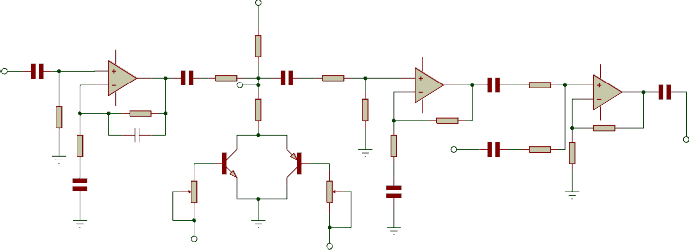
A schematic diagram that can be used to realise the block diagram of figure 1 is depicted in figure 2. The line amplifier is built around the operational amplifier (Op Amp) IC1 [1], [2], [3] and there is a further amplification after attenuation by IC3, while IC5 is the mixer amplifier.
The amplification of the MIC signal is done by IC2, while a further amplification by IC4 ensures enough signal level for rectification by the diodes. The positive half cycle of the signal is rectified by D2 and D3, while D1 and D4 rectify the negative half cycle. It is observed that distortion of the line signal results if only one half cycle is used for control. The transistors Q1 and Q2 form the controlled attenuator.
C1
Line Input
IC1
3 C5 R7
6
2 X
R9
C7 R11
IC3
3
6
2
C11
R21
IC5
3
6
2
C15
R5
R1
R3 C17
C3
R13 R15
Q1 Q2
R17
R19
A
C13 R23
R25
R27
R20
R22 C9
Mic Input C2
R2
IC2
3
6
2
R6
R4
C6 R8
2
3
IC4
R10
C8
6
R12 R16
D1 D2
C14
C4 C10 C12
D4 R14
D3 R18
![]()
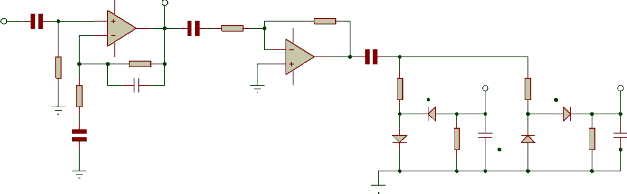
Fig.2: Schematic Diagram of the Voice-Controlled Amplifier
IJSER © 2012
Inte rnatio nal Jo urnal o f Sc ie ntific & Eng inee ring Re se arc h Vo lume 3, Issue 1, January -2012 3
ISS N 2229-5518
![]()
![]()
![]()
![]()
![]()
The Voice-Controlled Amplifier (VCA) is expected to be incorporated into existing systems. This implies that the input and the output signal levels should be compatible with commercially available audio equipments [4]. Thus the following specifications are obtainable:
Line input: 300mV, 10kΩ Mic. input: 20mV, 100Ω Output: 1V, 10kΩ
Frequency Response: 20Hz – 18 kHz.
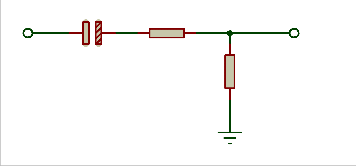
Each stage of the circuit can be isolated and analysed individually and then designed. Let us consider first the line input stage indicated in figure 3.
The circuit shown in Figure 3 is basically a non -inverting amplifier stage. The capacitor C3 controls the low frequency response while the high frequency response is controlled by C17. The capacitor C1 is chosen so that it has a very low reactance at the lowest frequency of interest. The gain of this amplifier stage is given by (1).![]()
![]()
![]()
Equation (4) can be expressed in the form![]()
The zeros of the gain function AF are located at![]()
![]()
The poles of this function are situated at![]()
![]()
Observation of (4) shows that This implies that the poles are located at frequencies lower than the zeros and the poles, therefore, control the frequency response of the amplifier stage. If component values are selected such that
C1
vl1 ![]()
R1
IC1
3
6
2
R5
R3 C17
v01
![]()
i.e. at – or 0.
In reality, however, the poles will be at – and
somewhere else near zero. It is also observed from (4) and![]()
(5) that![]()
C3
In the mid band frequency range C3 has nearly zero reactance while the reactance of C17 tends to infinity. The amplifier gain at mid band is, therefore given by (9).![]()
where![]()
Fig. 3: The line input amplifier![]()
It should be noted that the resistor R1 determines the input resistance of the stage and its value should be higher than the stated value of 10kΩ. Due to the symmetry of the circuit of Figure 2, the foregoing analysis is also applicable to the MIC amplifier.![]()
and![]()
When (2) and (3) are substituted into (1), we obtain
The schematic diagram of the mixer stage is shown in Figure 4. It should be observed that the signals and representing the outputs of the line and MIC amplifiers respectively vary in magnitudes and in opposite directions as indicated in Figure 5. This figure shows that when is
IJSER © 2012
Inte rnatio nal Jo urnal o f Sc ie ntific & Eng inee ring Re se arc h Vo lume 3, Issue 1, January -2012 4
ISS N 2229-5518
at maximum value, attains minimum value and vice- versa. Although may be as low as zero Volt, it is always expected that some value of be present under normal conditions of operation.
Equations (10) and (11) have been obtained at mid band where the effects of the capacitors on circuit performance are assumed to be negligible.
If then![]()
![]()
![]()
vl'
C11
R21
IC5
3
6
2
C15
and
vm'
C13 R23
R25
R27
The maximum value of each of and is fixed at
300mV. The minimum value of and is selected to be one-tenth of the maximum value, i.e. 30mV. It should be noted that and always vary in opposite directions so that when is maximum will be minimum. By substituting these values in (13) and knowing that the desired maximum value of is 1V, the values of R25 and R27 can be calculated.
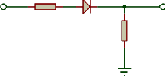
Figure 4: The mixer amplifier stage.
When the MIC input is zero, there is no output signal from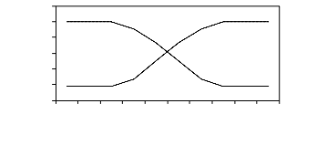
conducting (OFF) state and R13 is open -circuited at this end. The incremental voltage at point X (Figure 2) can be obtained from the circuit shown in figure 6.
C5
Figure 5: Signal variation of vi' and vm'
v01 vx
R9
The mixer amplifier should be designed so that there is always the possibility of contribution of both signals to the output. A non-inverting mixer is thus desired. The output signal in Figure 4 can be expressed as in (10).
Figure 6: Model for voltage at attenuator mid point. The voltage can be expressed as (14):![]()
![]()
![]()
![]()
![]()
The non-inverting input voltage is found by superposition to be![]()
![]()
![]()
The maximum value of is fixed to be 1.5V. The attenuation factor . The values of R7 and R9 are computed from these facts.
IJSER © 2012
Inte rnatio nal Jo urnal o f Sc ie ntific & Eng inee ring Re se arc h Vo lume 3, Issue 1, January -2012 5
ISS N 2229-5518
conditions stated above can be expressed as
vin
R16 D2
vc
![]()
R18
By selecting the value of to be one-third that of , the values of R11 and R15 can be computed. Similarly, by selecting the gain of IC3 to be, say, 3, the value of R17 and R19 are obtained.
The attenuation factor changes when the MIC input is at maximum value and this condition should be given a careful consideration. Under this condition the transistors Q1 and Q2 are both fully saturated so that the attenuation at point X is given by (16):![]()
![]()
![]()
![]()
where
The attenuation at mid band is given by (18):
Figure 7: Small signal rectifier circuit
If the components are chosen such that then
The maximum output of IC4 is fixed at a particular value, say 3V rms. The peak value corresponding to this maximum is then computed. The capacitor C12 (Figure 2) serves to maintain at the peak value.
The time constant should be selected to be small compared to the highest frequencies to be expected in the circuit in order to obtain a rapid discharge of C12 when the MIC input drops low. The criteria for the design of the negative half cycle rectification circuit are the same as for the positive half cycle.
When the output of IC4 is at positive maximum, the
transistor Q1 is fully saturated while transistor Q2 is saturated during the negative peak. The collector currents of Q1 and Q2 are assumed to be equal, i.e.
s o that![]()
Since the value of R7 has already been determined, if k is known (say 10% of 300mV) then the value of R9’ can be computed from which the values of R9 and R13 are obtained.
The voltage at the output of IC4 consists of both the
positive and negative half cycles. The positive half cycles are rectified by D2 while the negative half cycles are rectified by D1. Let us consider the operational circuit during the positive half cycles as given in figure 7. If we assume an ideal diode, when fully conductive, we have![]()
The base current of transistor Q1 is given by![]()
In order to obtain transistor saturation![]()
or![]()
![]()
The range of values of R20 that gives saturation of Q1 is therefore given by (23):![]()
It should be noted that in (20) to (23) the appropriate quantities with the subscripts ―sat‖ denote the saturation values. Similar equations can be written for the transistor Q2.
IJSER © 2012
Inte rnatio nal Jo urnal o f Sc ie ntific & Eng inee ring Re se arc h Vo lume 3, Issue 1, January -2012 6
ISS N 2229-5518
If R20 is chosen to be too low, there will be saturation even at much smaller values of Vc. R20 should be made varia ble and set as appropriate during final circuit adjustments.
The circuit given in figure 2 was designed and built in accordance with the specifications and analysis. The circuit was simulated using Multisim version 10.0.1 [6]. The following tests were carried out on the complete circuit to verify the performance.
The voltage of 300 mV was fed to the line input (with the
MIC input grounded) and the frequency response of the line amplifier was measured. This is shown in figure 8.
A signal level varied between 0 mV to 60 mV was fed at the MIC input and the output of IC3 was measured (with the line input fixed at 300 mV, 5 kHz) at each setting of the input signal in order to determine the attenuation effect. Figures 9 and 10 show the measurements obtained.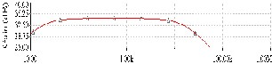
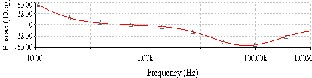
Fig. 8: Frequency Response of the Line Amplifier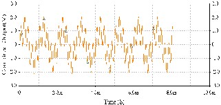
Fig. 9: Combined effects of Mic and Line signals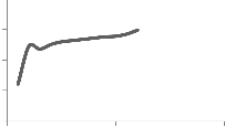
4
3
2
1
0
0 50 100
MIC Input (mV)
Figure 10: Attenuation of Line Input by MIC Signal
The detailed analysis of a Voice-Controlled Amplifier that uses the bipolar junction transistor for attenuation has been presented. The circuit designed was tested and the results agree closely with the design specifications and analysis presented. The circuit will be of great use in many environments requiring simultaneous audio signal transmission.
[1] J. Millmanand A. Grabel, Microelectronics, McGraw- Hill Book
Company, New York, 1988.
[2] Neamen, D. A, ElectronicCircuit Analysis and Design, McGraw- Hill
Book Company, New York, 1996.
[3] Holt, C.A, Electronic Circuits, Digital and Analog, John Wiley and Sons
Inc., New York, 1978.
[4] Howard, M.T, Audio Encyclopaedia, Howard W. Sams and
Company
Inc., Indiana, 1969.
[5] Kuo, F.F. Network Analysis and Synthesis, JohnWiley and Sons
Inc., New York, 1977.
[6] Multisim (Version10.0.1) User Guide, National Instruments,
11500 North Mopac Expressway, AustinTexas, January, 2007.
Engr. Dr. Jonathan A. Enokela is a professionally registered engineer. He lectures in the Department of Electrical and Electronics Engineering, Federal University of Agriculture, Makurdi, Nigeria. Email: jenokela@yahoo.com
Engr. Dr. Jonathan U. Agber is a professionally
registered engineer. He lectures in the Department of
Electrical and Electronics Engineering, Federal University of Agriculture, Makurdi, Nigeria. Email: jonagber@yahoo.co.uk
IJSER © 2012