International Journal of Scientific & Engineering Research, Volume 6, Issue 3, March-2015 801
ISSN 2229-5518
A Novel Low Current Ripple Magnetically Coupled Interleaved DC-DC Buck-Boost Converter with High Efficiency and Continuous Transfer- Function for Fuel-Cell Applications
V.Samavatian, F.Mardani, M.Nourmohammadpour
Abstract— Efficiency, steady state analysis along with dynamic operation discussion of DC-DC converters are undoubtedly important issues in proficiency of renewable energy exploitation. This paper demonstrates the feasibility of using a DC-DC magnetically coupled interleaved DC-DC buck-boost converter for fuel-cell applications. While a step-up/step-down voltage transfer ratio has been achieved, the proposed converter exhibits non-pulsating I/O currents using interleave technique making it very suitable for renewable applications. Besides thoroughly elaboration of the steady state analysis, dynamic analysis including the converter control-to-output transfer function, which is continuous between two operation modes using I/O magnetic coupling, and a small signal ac equivalent circuit model based on state space averaging (SSA) method is also presented to help the designing of closed loop controllers for this proposed converter. Furthermore the experimental results are presented to verify the theoretical expected merits of the converter including high efficiency, non- pulsating I/O currents and continuous control-to-output transfer function. These Experimental results show impressive benefits of the proposed converter.
—————————— ——————————
ith ever-increasing use of renewable energy, crucial role of power electronic converters and their controlling methods have become fully evident in recent years. Studying and designing these converters is one of the most pressing con- cerns facing all electrical engineers. One of these converters ex- tensively used in renewable energy resources such as battery charging, fuel cell systems, power factor correction (PFC), hy- brid electric vehicles, communication power supply, maximum power point tracking (MPPT) of photovoltaic system (PVs) and for other renewable sources’ maximum energy extraction, is DC-DC converters. Generally DC-DC converters divided into three main parts: buck, boost and buck-boost. Buck-boost con- verter has been employed since output voltage is within unreg-
ulated input voltage [1-9].
Despite conventional single-active-switch Buck-boost converter
topologies including SEPIC, CUK, conventional inverting buck-
boost and Flyback, non-inverting boost-buck converter made by cascaded connection of a boost converter to the buck converter is also achievable. It is indicated that this converter could be a reasonable choice in renewable energy power extractions due to
————————————————
• Vahid Samavatian received the M.S. degree from K.N.Toosi University of Technology, Tehran, Iran, and He is currently working toward the Ph.D. degree in the University of Tehran, Tehran, Iran
E-mail: vahidsamavatian@ee.kntu.ac.ir
• Fatemeh Mardani Received the M.S. degree in Electrical Engineering, Elec- trical Machine & Power Electronics, from the K.N.Toosi University of
Technology, Tehran, Iran.
![]()
E-mail: fateme.mardani68@gmail.com
• Mohammad Nourmohmmadpour received the M.S. degree in Electrical
Engineering, Electrical Machine & Power Electronics, from K. N.Toosi
University of Technology, Tehran, Iran.
![]()
E-mail: m.nourmohammadpour@ee.kntu.ac.ir
its high efficiency and low component stresses in comparison with conventional single-active-switch buck-boost converters [2,3]. Beside above-mentioned step-up/step-down DC-DC con- verter topologies, a single inductor buck-boost converter which has high performance in the low voltage applications is thor- oughly discussed in [5-7]. Regarding its topology, this converter is not suitable for high voltage/power applications. Another topology is KY buck–boost converter removing barrier of right half plane (RHP) zeros at the expense of increasing the number of switches resulting in increasing the cost of the device [10,11]. Most of the DC-DC converters mentioned earlier have the det- riment of pulsating input/output (I/O) currents resulting in high noise level and complicated controlling system [3,4].In many applications low-ripple I/O current is absolutely essential espe- cially in hybrid electric vehicles, power factor correction, fuel cell, etc [12-14]. The two-switch tri-state buck-boost has been used in order to mitigate this problem [15] and regarding capa- bility of using large inductance in pseudo-continuous conduc- tion mode (PCCM) [16], [17], lower-ripple I/O currents can be readily achieved. However efficiency of this converter declines owing to the increase in the number of active switches. Using interleaved technique including the benefits such as harmonic cancellation, better efficiency, component stresses reduction, better thermal performance, and high power density is another solution that can be easily acquired [12, 14, 18-21]. Although the concept of this technique is not newly introduced, wide areas of applications are covered by this technique [22]. In [12], the 16- phase interleaved bidirectional boost topology for hybrid ener- gy storage system (HESS) has solved I/O currents high ripple but this topology has just discussed the boost converter and it is
IJSER © 2015 http://www.ijser.org
International Journal of Scientific & Engineering Research, Volume 6, Issue 3, March-2015 802
ISSN 2229-5518
not generalized in buck-boost converters. In [14], H.K. Liao et al, have proposed an interleaved non-inverting buck-boost con- verter with a low-output current ripple, but in this topology
mitigating the input voltage variation in wide range is not achieved. Although the double-switch buck–boost converter proposed in [19] can reduce the current ripple, component stresses have been remained high through this topology result- ing in low efficiency. Another solution reported here is to utilize a non-inverting interleaved buck-boost converter. This pro- posed topology is used in order to improve I/O currents ripple, converter ’s efficiency and reduce component stresses. In addi- tion, because input and output inductances are magnetically related to each other, the small signal control-to-output transfer function dissociation at boundary mode of proposed converter which is a major problem in double-active-switch buck-boost converters is readily solved. This proposed converter can be easily used as a modular converter suitable for high transferring power density. The purpose of this paper is to analyze cascaded combination of an interleaved boost with an interleaved buck converter magnetically coupled and shown in Fig. 1. Organiza- tion of this paper is as follows. Section II discusses principle of operation and steady state analysis based on the depicted key
Fig. 2. Operating modes of proposed converter: (a) boost mode; (b) buck mode.
The steady state operation waveforms of this converter for both modes of boost and buck are illustrated in Fig. 3(a) and (b) re-
waveforms of proposed converter. Dynamic Analysis and small
signal modeling are thoroughly studied in section III. In section
spectively. The last curves in these two figures,
S1 to
S 4 , are
IV, circuit design and its implementation have been presented.
allocated to logic activation signals of Q1 to Q 4 The PWM acti-
Section V focuses on the experimental results in both operation
modes and under different conditions. Finally, the last section
vation signals of
Q1 and Q 2
are similar to each other with a
presents conclusion of this study.
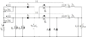
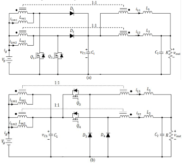
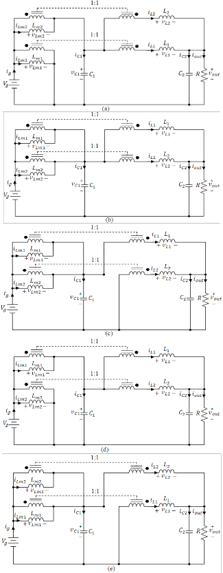
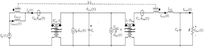
Proposed converter is shown in Fig. 1. This converter can oper- ate either in boost mode or buck mode as shown in Fig. 2(a) and Fig. 2(b) respectively. As shown in Fig. 2 the boost mode would be achieved provided that the switches 3 and 4 are permanently turning on and switches 1 and 2 working in PWM manner, while in the buck mode switches 1 and 2 are permanently turn- ing off and switches 3 and 4 working in PWM manner.
Fig .1. Schematic circuit diagram of proposed converter
phase shift of Ts / 2 for catering the interleaved pattern. In the
boost mode the duty ratios of the boost stage ( Q1 and Q 2 activa- tion signals) are considered to be d12 (t ) . The same is true for Q3 and Q 4 activation signals with the duty ratio d 34 (t ) in the buck mode. The duty ratio of switches is adjusted so that the output voltage is regulated around a desired value (here 36 V) in both operational modes. In addition, through increasing the number of interleaved phase in boost and buck stages, the pro- posed converter can be easily used as a modular converter be-
ing suitable for transferring high power density in applications
such as HESS and other individual storage systems. For extract-
ing the principles of operation and determining the modeling equations for both modes of operation, the switching pattern of Fig. 4 is employed. By resorting this switching pattern, all pos- sible converter switching states will be considered. Regarding this figure, each period consists of 6 time intervals and 6 corre- sponding circuit diagrams depicted in Fig. 5. Time interval numbering and portioning are mentioned in Table. 1. Since the intervals 2 and 5 have the same time portions and switching states, (see Fig. 4 and Fig. 5), the converter can be analyzed only in 5 states as follows:
Interval 1:[ t 0 − t1 ], Fig. 5(a), In this time interval Q1 , Q3 and Q 4
are in conducting mode making the magnetizing inductor 1 to
IJSER © 2015 http://www.ijser.org
International Journal of Scientific & Engineering Research, Volume 6, Issue 3, March-2015 803
ISSN 2229-5518
start saving energy and simultaneously magnetizing inductor 2 to transfer its stored energy to the output load and inductors
Interval 3: [ t 2 − t 3 ], Fig. 5(c), in this time interval Q3
is in con-
ducting mode while Q1 , Q 2 and Q 4
are off. Energy transfer in
through D 2 . With regard to Fig. 5(a), the differential equations
describing the voltage across the capacitors and current passing
through the inductors in the first time interval can be evaluated as follows:
this interval is thoroughly similar to the previous interval ex- cept that the energy stored in both input magnetizing inductors is only transferred to the inductor 1.
Interval 4: [ t 3 − t 4 ], Fig. 5(d), in this time interval Q 2 , Q3 and Q 4
are conducting while Q1
is turning off. Energy transfer in this
interval is also similar to that of interval 1 except that the func- tions of magnetizing inductors 1 and 2 replace each other.
Interval 6: [ t 5 − t 6 ], Fig. 5(e), in this time interval Q 4
is in con-
ducting mode while Q1 , Q 2 and Q3 are off. Accordingly the en- ergy saved in magnetizing inductor 1 and 2 is transferred to the output capacitor and inductor 2.
Interval 2 and 5: [ t1 − t 2 and t 4 − t 5 ], Fig. 5(b), in this time inter-
Table.1. required expressions for evaluating parameters’ values
val Q3
and Q 4
are in conducting mode while Q1
and Q 2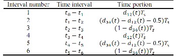
are
turning off. Accordingly the energy stored in magnetizing in- ductors 1and 2 starts transferring to inductors 1 and 2 through D1 and D 2 . Similarly, a set of differential equations can be
found for describing the voltage across the capacitors and cur-
rent passing through the inductors for other time intervals, but for briefness these equations have not been written.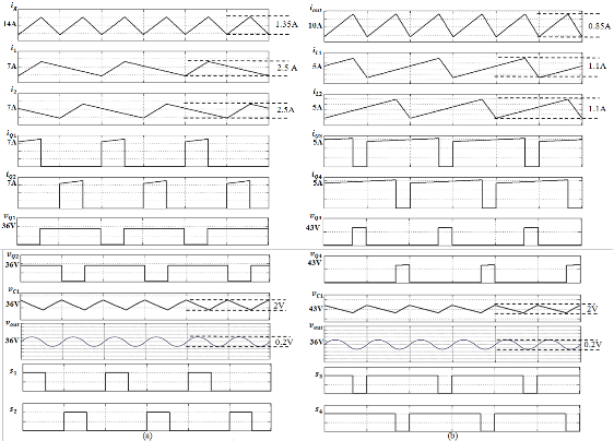
Fig. 3. Key waveforms of converter shown in Fig. 1 for V out
= 36 V
, (a) currents and voltages in boost mode with V g
= 26 V ( D34 =1 ), (b) currents and
voltages in buck mode with V g
= 43 V
( 12 = 0 )
IJSER © 2015 http://www.ijser.org
International Journal of Scientific & Engineering Research, Volume 6, Issue 3, March-2015 804
ISSN 2229-5518
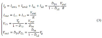
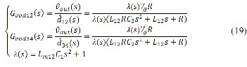
The last expression of equation 3 is the voltage transfer ratio of converter M ( D1 , D 2 ) as follows:
![]()
Fig. 4. Switching pattern of converters’ switches
To the authors’ knowledge two reported methods are em- ployed for obtaining the differential equations portraying the behavior of all interleaved converters, namely, state space av- eraging (SSA) methods [16] and signal flow graph (SFG) [37]. In this work state space averaging method is selected owing to its simplicity.
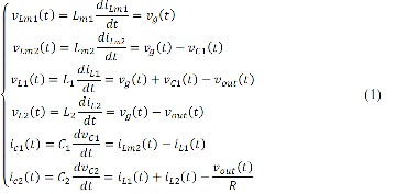
With the assumptions of continuous conduction mode (CCM)
working and a switching frequency much higher than the converter natural frequencies, SSA method [16] can be applied to determine the converter model regarding the small-ripple approximation and the principles of inductor volt-second bal- ance and capacitor charge balance.
Using the differential equations of all time intervals and exert- ing averaging technique [16] on evaluated equations over one switching period, it yields: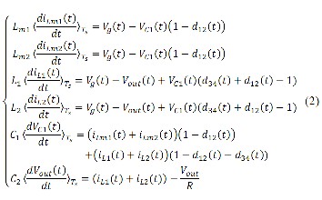
Where d12 and d 34 are the duty ratios of the switches [Q1 , Q 2 ]
The converter operation in both boost and buck modes is de-
fined by the following conditions.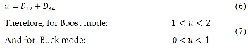
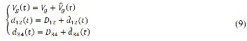
For a smooth transition between the two modes of operation, voltage transfer ratio M ( D12 , D 34 ) should be written in terms of only one control variable [17], [19]. To establish a meaning- ful relation between D12 and D 34 , the variable u is defined:
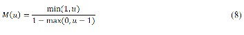
Regarding this new variable, the modified voltage conversion ratio can be written as follows.
Employing equation (8) as voltage conversion ratio, a smooth transition between the two modes of operation can be easily guaranteed. The voltage conversion ratio in term of u is illus- trated in Fig. 6.
and
[Q3 , Q 4 ] respectively. For attaining the current passing
through the converter inductors and the voltage across the converter capacitors in steady states condition, one may use
the steady state operating value of duty ratios,
D12 and D 34 ,
Fig. 6.Voltage Conversion ratio of the proposed buck-boost converter
and input voltage, V g , and exert the principles of inductor
volt-second and capacitor charge balance to obtain another set of expressions describing the steady state operation as follows:
IJSER © 2015 http://www.ijser.org
International Journal of Scientific & Engineering Research, Volume 6, Issue 3, March-2015 805
ISSN 2229-5518
To obtain the small signal model around the specific operating
point, the input voltage,V g (t ) , and duty ratios,
d12 (t )
and d 34 (t ) , are assumed as a constant value of V g , D1 and D 2
plus some small ac variations, Vˆ (t ) ,
dˆ (t )
and
dˆ (t ) re-
spectively.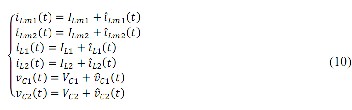
By applying above inputs, the inductor currents and capacitor voltages can be stated with their steady state plus their small ac variations determined by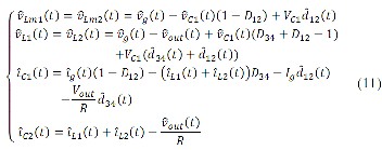
Now the set of differential equations (2) can be linearized around their operating point values providing that the ac vari- ations are much smaller than the steady state values at operat- ing point. Employing this analysis along with separating just first-order terms of resulted equations, following set of equa- tions of inductor voltages and capacitor currents can be readi- ly acquired.
Regarding (11), one can consider an input and output induc-
tors whose values are equal to the value of L m 1 and L m 2
and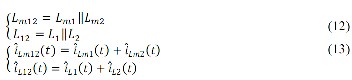
L1 and L 2 connecting in parallel respectively. Let us define:
Now with using (11), the small signal ac equivalent circuit model can be obtained [3]. Fig. 7 illustrates small signal ac equivalent circuit model of proposed converter.
By above definition and defining state space vector xˆ
as (14)
Fig. 5.Operating states. (a) circuit diagram in interval 1,(b) circuit diagram in interval 2,5,(c) circuit diagram in interval 3, (d) circuit diagram in interval
4, (e) circuit diagram in interval 6.
and state space equation as (15) and by linearizing (2) around (3) and separating just first-order terms of resulted equations, it yields
IJSER © 2015 http://www.ijser.org
International Journal of Scientific & Engineering Research, Volume 6, Issue 3, March-2015 806
ISSN 2229-5518
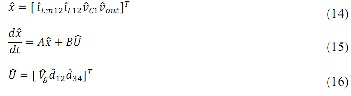 can be given by following expressions respectively. Where A is state matrix and B is input vector corresponding to
Vˆ , dˆ (t ) and dˆ (t ) .
g 12 34
With regard to the above equations, continuous behavior is
achieved between two operation modes using magnetic cou-
pling. Employing the following parameter values (completely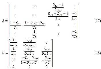
explained in the following section),
L m 12 = 100m H ,
L = 100
12
m H , C
1 = C 2
= 10mf
and
R = 3.6Ω , the bode dia-
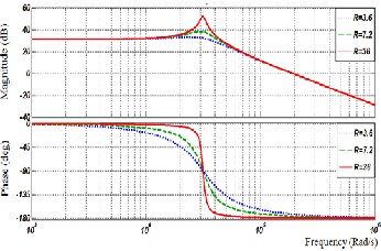
gram of control-to-output transfer functions in boundary mode is depicted in Fig. 8 in terms of three different load con- ditions R = 3.6Ω , R = 7.2Ω and R = 18Ω . It is easily seen that in this mode phase margin (PM) is not large enough to guar- antee the stability of closed loop system. This problem can be easily solved by designing a suitable classic controller. Fur- thermore by increasing load to its nominal value, it can also be observed that in this mode PM would be boomed.
Accordingly in the boundary mode, namely D12
and D 34 are
equal to 0 and 1 values respectively, the small signal control-
ˆ ˆ
to-output transfer functions with respect to d12 (t ) and d 34 (t )
Fig. 7. Small signal ac equivalent circuit model for converter
The proposed converter is designed as fuel cell regulation de- vice so that its input voltage range varies from 26V to 43V. The maximum output power is 360W. Regarding output voltage value, 36V, corresponding load resistance is 3.6 Ohm By above data it can be easily observed that duty ratios are limited to
0 < D
12
< 0.2777 and 0.833 < D34 < 1
in boost and buck opera-
Fig. 8. Frequency response of the small-signal control-to-output transfer function in the boundary mode.
tion modes respectively. The switching frequency is fixed around 25 KHz and as a consideration the inductors currents ripples are restricted to 1.5A while output capacitor and in- termediate capacitor voltage ripples are respectively limited to
0.2 V and 2V. Expressions required for calculating values of
capacitors and inductors in both operation modes can easily
obtained from differential equations described in section II
IJSER © 2015 http://www.ijser.org
International Journal of Scientific & Engineering Research, Volume 6, Issue 3, March-2015 807
ISSN 2229-5518
and the final circuit design equations listed in Table. 2.
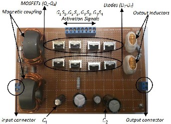
Fig. 9 has shown the top view of power stage prototype. The components have been individually introduced on this figure. In this section, the behavior of proposed converter in the steady state condition with applying V g equal to 26V in boost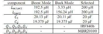
mode and 43V in buck mode under full load condition will be discussed. Furthermore, dynamic responses led by load and input voltage changes will be separately studied in two differ- ent operation modes. The design matches a fuel cell voltage regulation, with the brand of “FCgen 1020ACS” Ballard Power Systems, Inc. regarding design equations, the components list and their values are given in Table. 3.
Employing Fig. 8 and classical rules of designing a linear compensation network in frequency domain [3] for increasing the stability margin in both operation modes, the following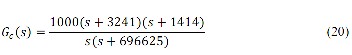
second-order compensator transfer function can be evaluated.
The circuit diagram of the above compensator and the pulse width modulation (PWM) are depicted in Fig. 10 where switching dispositions has been added for catering interleaves technique. One should notice that by considering this circuit diagram an effective analogue controller for the converter can be easily achieved using a few conventional simple compo- nents.
Table.3. Components for proposed converter
Table. 2 Expressions required for calculating converter values in CCM
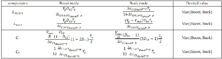
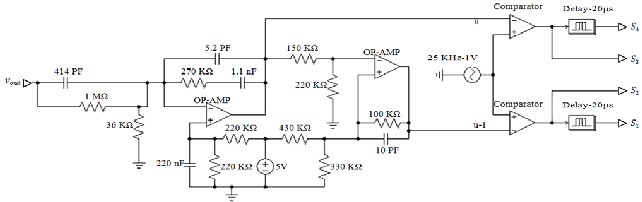
Fig. 10.Schematic of compensation network using analogue circuit
IJSER © 2015 http://www.ijser.org
International Journal of Scientific & Engineering Research, Volume 6, Issue 3, March-2015 808
ISSN 2229-5518
 (a)
(a)
Fig. 9. Proposed converter prototype
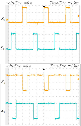
The activation signals in boost mode are depicted in Fig. 11a
where
D34 = 1
and 12
are operating in PWM mode and
D = and D are oper-
those are shown in Fig. 11b where 12 0 34
ating in PWM mode respectively. As it can be seen in Fig. 11 the activation signals either in boost mode or in buck mode have a delay of Ts / 2 . This delay guarantees the procedure of
interleaving technique which is one of the most important
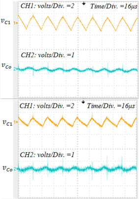
aims of this proposed converter. Figs. 12a and 12b show the input, output and inductor currents in boost and buck opera- tion modes respectively. As illustrated from these figures, the maximum ripple is limited to 1.5A for the inductor currents (%11.5) and to 1A (%10) for input and output currents respec- tively. The voltage ripples of intermediate capacitor and out- put capacitor in both operation modes are depicted in Figs.
13a and 13b. Maximum ripple of intermediate capacitor and
output capacitor voltages are restricted to 2V, 0.2V (%0.5), re- spectively. Not only these properties satisfactorily meet the application requirements, but also when compared to the oth- er recent studies [4], [11], [14], [16] with input current ripple percentages as large as %20, %23, %30 and %30 respectively, proves an enhanced steady state performance for this convert- er. The dynamic behaviors of this converter during applying a load change between half rated (180W) and full rated (360W) for both boost and buck operation modes are depicted in Fig.
14(a) and Fig. 14(b) respectively. Employing compensation
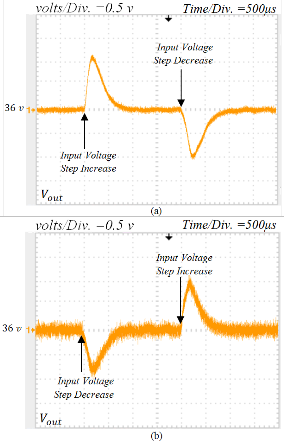
network given in (20), one can find that only a voltage change of 1.8V (5%) in boost mode and about 2.5V (6.9%) in buck mode occurs once the load change is applied and the converter encounters no internal oscillation. The dynamic responses of proposed converter output voltage to large input voltage vari- ation under full load condition are illustrated in Fig. 15. In boost mode, input voltage increases from 26V to 36V and then decreases to its initial value while in buck mode input voltage decreases from 43V to 36V and then increases to its initial val- ue. This figure depicts that the maximum overshoot is strictly kept less than 1.1V (3%) in both operation modes.
(b)
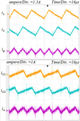
Fig. 11.Activation signals, (a) boost mode, (b) buck mode
(a)
(b)
Fig. 12. Converters’ currents, (a) boost mode, (b) buck mode
IJSER © 2015 http://www.ijser.org
International Journal of Scientific & Engineering Research, Volume 6, Issue 3, March-2015 809
ISSN 2229-5518
(a)
(b)
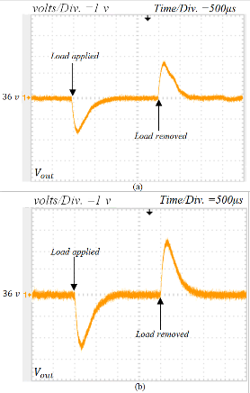
Fig. 13. Converters’ voltages, (a) boost mode, (b) buck mode
Fig. 15. Output voltage variations during input voltage step changes, (a)
boost mode, (b) buck mode.
The energy conversion efficiency is a major issue of any con- version system. Efficiency traces as a function of the input voltage for different output current levels are shown in Fig. 16. Regarding this figure, Maximum efficiency as a function of the input voltage with different output current levels occurs in all current levels when input voltage is near to 36 V. Because in this case, buck and boost switches are permanently on and off respectively and there is only conduction power loss.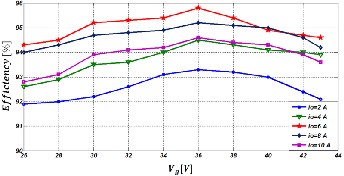
Fig. 14. Output voltage variations during applying and removing load from its half rated (180W ) to its rated (360W ). (a) Boost mode, (b) Buck mode.
Fig. 16. Energy conversion efficiency for Vo= 36 V as function of the input voltage for different output current levels.
A non-inverting I/O magnetically coupled buck–boost DC–DC converter obtained through a cascade connection of an inter- leaved boost and an interleaved buck stage, is discussed.
IJSER © 2015 http://www.ijser.org
International Journal of Scientific & Engineering Research, Volume 6, Issue 3, March-2015 810
ISSN 2229-5518
Mathematical analyses, simulation and experimental results of a prototype converter validate the predicted low-ripple I/O currents due to interleaved technique employment. Efficiency studies show that the maximum efficiency can be achieved in the boundary mode where the boost stage switches are al- ways OFF and the buck stage switches are continuously ON.In addition, converter small signal modeling is explored to help the control design. Dynamic studies show that the maximum overshoot is limited to 7% in the load changes while it is about
3% in the input voltage changes. The output voltage is well
adjusted and made stiff from severe input voltage variations in both operation modes using a simple compensator. In compar- ison with some conventional topologies the part counts of proposed converter have been increased. However, converter reliability and small size of these components resulted from using interleave technique have compensated this detriment. Dynamic stiffness along with the capability of low-ripple I/O currents make this converter very attractive for many renewa- ble applications like fuel cell, battery, super-capacitor, PV pan- el, or fuel cell energy exploitation. There is still one remaining small problem associated with the proposed converter, namely RHP zeros in the boost mode being worked to be solved and reported in the near future.
[1] Ren, X.Y., Tang, Z., Ruan, X.B., Wei, J., Hua, G.C.: ‘A novel fourswitch buck–boost converter’, Proc. CSEE, 2008, 28, (21), pp. 15–19
[2] Samavatian, V; Radan, A, "A novel low-ripple interleaved buck-boost converter with high efficiency and low oscillations for fuel cell applica- tions,” Int J Electr Power Energy Syst, vol.63, pp.446, 454, Dec. 2014.
[3] R. W. Erickson and D. Maksimovic, Fundamentals of Power Electronics,
2nd ed. Norwell, MA: Kluwer, 2001.
[4] Carlos Restrepo, Javier Calvente, Angel Cid-Pastor, Abdelali El Aroudi, and Roberto Giral, ‘‘A Non-Inverting Buck-Boost DC-DC Switching Con- verter with High Efficiency and Wide Bandwidth,’’.IEEE TRANSAC- TIONS ON POWER ELECTRONICS, VOL. 26, NO. 9, SEPTEMBER 2011
[5] P.-C. Huang, W.-Q.Wu, H.-H.Ho, and K.-H. Chen, “Hybrid buck-boost feed forward and reduced average inductor current techniques in fast line transient and high-efficiency buck-boost converter,” IEEE Trans. Power Electron., vol. 25, no. 3, pp. 719–730, Mar. 2010.
[6] Y.-J. Lee, A. Khaligh, A. Chakraborty, and A. Emadi, “Digital combina- tion of buck and boost converters to control a positive buck-boost convert- er and improve the output transients,” IEEE Trans. Power Electron., vol. 24, no. 5, pp. 1267–1279, May 2009.
[7] Y.-J. Lee, A. Khaligh, and A. Emadi, “A compensation technique for smooth transitions in a noninverting buck-boost converter,” IEEE Trans. Power Electron., vol. 24, no. 4, pp. 1002–1015, Apr. 2009.
[8]S. Waffler and J. Kolar, “A novel low-loss modulation strategy for high power bidirectional buck + boost converters,” IEEE Trans. Power Electron., vol. 24, no. 6, pp. 1589–1599, Jun. 2009.
[9] X. Ren, X. Ruan, H. Qian, M. Li, and Q. Chen, “Three-mode dual fre- quency two-edge modulation scheme for four-switch buck-boost convert- er,” IEEE Trans. Power Electron., vol. 24, no. 2, pp. 499–509, Feb.2009.
[10] K. I. Hwu and Y. T. Yau, “Two types of KY buck–boost converters,”
IEEE Trans. Ind. Electron., vol. 56, no. 8, pp. 2970–2980, Aug. 2009.
[11] Hwu, K. I.; Peng, T. J., "A Novel Buck–Boost Converter Combining KY
and Buck Converters," Power Electronics, IEEE Transactions on , vol.27, no.5,
pp.2236,2241, May 2012.
[12]Blanes, J.M.; Gutierrez, R.; Garrigos, A.; Lizan, J.L.; Cuadrado, J.M.,
"Electric Vehicle Battery Life Extension Using Ultracapacitors and an FPGA Controlled Interleaved Buck–Boost Converter," Power Electronics, IEEE Transactions on , vol.28, no.12, pp.5940,5948, Dec. 2013
[13]Younghoon Cho; Jih-Sheng Lai, "High-Efficiency Multiphase DC–DC Converter for Fuel-Cell-Powered Truck Auxiliary Power Unit," Vehicular Technology, IEEE Transactions on , vol.62, no.6, pp.2421,2429, July 2013 [14]Liao, H.-K.; Liang, T.-J.; Yang, L.-S.; Chen, J.-F., "Non-inverting buck– boost converter with interleaved technique for fuel-cell system," Power Electronics, IET , vol.5, no.8, pp.1379,1388, September 2012 doi: 10.1049/iet-pel.2011.0102
[15]Mingzhi He; Fei Zhang; JianpingXu; Ping Yang; Tiesheng Yan, "High- efficiency two-switch tri-state buck-boost power factor correction convert- er with fast dynamic response and low-inductor current ripple," Power Electronics, IET , vol.6, no.8, pp.1544,1554, September 2013
[16] Ma, D., Ki, W.: ‘Fast-transient PCCM switching converter with free wheel switching control’, IEEE Trans. Circuits Syst. II, Express
Briefs, 2007, 54, (9), pp. 825–829
[17]Viswanathan, K., Oruganti, R., Srinivasan, D.: ‘Dual-mode control of tri-state boost converter for improved performance’, IEEE Trans.
Power Electron, 2005, 20, (4), pp. 790–797
[18]Cai-Yang Ko; Tsorng-Juu Liang; Kai-Hui Chen; Jiann-Fuh Chen, "De- sign and analysis of an interleave controlled series buck converter with low load current ripple," Circuits and Systems (APCCAS), 2010 IEEE Asia Pacific Conference on , vol., no., pp.672,675, 6-9 Dec. 2010
[19] Xiao, H.; Xie, S., "Interleaving double-switch buck-boost converter,"
Power Electronics, IET, vol.5, no.6, pp.899,908, July 2012
[20] Po-Wa Lee; Lee, Y. -S; Cheng, D.K.-W.; Xiu-Cheng Liu, "Steady-state analysis of an interleaved boost converter with coupled inductors," Indus- trial Electronics, IEEE Transactions on , vol.47, no.4, pp.787,795, Aug 2000
[21] Hajizadeh, A.; Golkar, M.A.; Feliachi, A., "Voltage Control and Active Power Management of Hybrid Fuel-Cell/Energy-Storage Power Conver- sion System Under Unbalanced Voltage Sag Conditions," Energy Conver- sion, IEEE Transactions on , vol.25, no.4, pp.1195,1208, Dec. 2010
[22] Miwa, Brett A.; Otten, D.M.; Schlecht, M.F., "High efficiency power
factor correction using interleaving techniques," Applied Power Electronics Conference and Exposition, 1992. APEC '92. Conference Proceedings 1992., Seventh Annual,vol., no., pp.557, 568, 23-27 Feb 1992
[23]J. Calvente, L. Martinez-Salamero, P. Garces, and A. Romero, “Zero dynamics-based design of damping networks for switching converters,” IEEE Trans. Aerosp. Electron. Syst., vol. 39, no. 4, pp. 1292–1303, Oct. 2003. [24]Veerachary, M., "General rules for signal flow graph modeling and analysis of dc-dc converters," Aerospace and Electronic Systems, IEEE Trans- actions on , vol.40, no.1, pp.259,271, Jan 2004
[25] Veerachary, M., "Modeling of Power Electronic Systems Using Signal Flow Graphs," IEEE Industrial Electronics, IECON 2006 - 32nd Annual Con- ference on , vol., no., pp.5307,5312, 6-10 Nov. 2006
[26] Veerachary, M.; Senjyu, T.; Uezato, K., "Signal flow graph modelling of DC-DC parallel converter with coupled inductors," Power Conversion Conference, 2002. PCC-Osaka 2002. Proceedings of the, vol.3, no., pp.1352,
1356 vol.3, 2002
[27] Veerachary, M., "Analysis of interleaved dual boost converter with integrated magnetics: signal flow graph approach," Electric Power Applica- tions, IEE Proceedings - , vol.150, no.4, pp.407,416, 8 July 2003
[28] Veerachary, M.; Senjyu, T.; Uezato, K., "Signal flow graph nonlinear modelling of interleaved converters," Electric Power Applications, IEE Pro- ceedings - , vol.148, no.5, pp.410, 418, Sep 2001
[29] Veerachary, M.; Senjyu, T.; Uezato, K., "Signal flow graph nonlinear modeling analysis of IDB converter [interleaved dual boost]," Industrial Electronics, 2001. Proceedings.ISIE 2001. IEEE International Symposium on, vol.2, no., pp.1066, 1070 vol.2, 2001
IJSER © 2015 http://www.ijser.org