International Journal of Scientific & Engineering Research, Volume 4, Issue 10, October-2013 1057
ISSN 2229-5518
Wireless Power Transfer Using Resonant Inductive
Coupling for 3D Integrated ICs
Akancha Srivastava Khare1, Ashish Mishra2, Abhishek Kr. Mishra3
M. Tech. Scholars1, 2, 3
Chandra Mohan Jha University Meghalaya INDIA1, MPEC Kanpur (U.P.) INDIA2, KIT Kanpur (U.P.) INDIA3
@: srivastava_akancha@yahoo.in1, @: ashishsitm18@gmail.com2, @engrabhishek786@gmail.com3
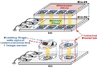
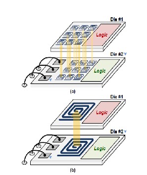
3 D integration is a promising solution for shortening interconnects in parallel processing in order to achieve smaller form-factor and higher performance. Several wired and wireless methods have been proposed to implement data communication among vertically stacked IC’s in a package [1, 2]. However, only wired methods such as wire-bonding or micro-bumps have been used for the power supply, even though wireless power delivery has unique advantages in 3D IC’s applications. It can eliminate the Known-Good-Die (KGD) issues to improve the yield, and some MEMS applications require non-contact power transfer [3], which can be realized by wireless power transfer. Fig.1 illustrates two examples of systems requiring wireless power transfer.
Previous work has reported wireless power transmission
between two inductively coupled coils in stacked dies with in a package [4]. This uses standard inductive coupling which results in relatively low power efficiency (<30%) and large coils (700x700µm) since most of flux is not linked between the coils. The resonance of an inductively coupled system increases the amount of magnetic flux linked between coils and improves the power transmission significantly. In this paper we will introduce wireless power transfer using resonant inductive coupling for 3D IC’s to increase power transfer efficiency and density with smaller coils.
The paper is organized as follows; In Section II, we will discuss power transfer efficiency. The optimal condition and numerical analysis on maximum power transfer efficiency will be introduced. Section III discusses power transfer density. In IC designs, silicon area are always a major concern. Therefore, power density is sometimes more critical than power efficiency inside a package. We will discuss the optimal values for coil
size, load resistance, and coupling coefficient k for maximum power transfer density. Section IV will show the coil design for an inductive power link and the simulation results of power efficiency and density. Section V concludes the paper.
Fig. 1. The applications of wireless power transfer using inductive coupling:
(a) Vertical stacking of heterogeneous processes such as
logic and DRAM
(b) Information Tethered Micro Automated Rotary
Stages (ITMARS).
A. Equivalent Circuit
Fig. 2 shows the concept of an inductive power link and its equivalent circuit. The RF input signal with a power amplifier in the transmitter is modeled as a voltage source in the primary resonator. The receiver is modeled as a resister RL in the secondary resonator. k is the transformer coupling coefficient, and L1 and L2 are self-inductance in transmitter and receiver Coils, respectively. R1 and R2 model the losses in the coils. C1 and C2 are capacitors including parasitic and external capacitance to create a resonance at the transmitter and receiver side. Standard inductive coupling uses a frequency well below the self-resonant frequency of the inductors, therefore parasitic
capacitance (C1 , C2 ) are typically ignored in this case. Resonant
IJSER © 2013 http://www.ijser.org
International Journal of Scientific & Engineering Research, Volume 4, Issue 10, October-2013 1058
ISSN 2229-5518
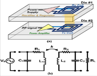
inductive coupling, however, uses this capacitance to resonate with the inductors, increasing the flux linked between transmitter and receiver.
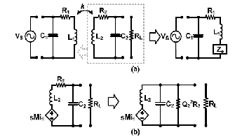
Fig. 3. (a) Entire equivalent circuit (b) Secondary equivalent circuit
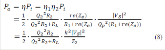
Combining (2) and (3), the total power efficiency of the inductive power link is derived as a form similar to [6-8].
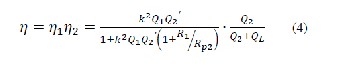
Fig. 2. (a) Concept of wireless inductive power link (b) Equivalent circuit
B. Analysis with Equivalent Circuit
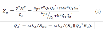
As shown in Fig. 3 (a), the circuit with a transformer can be converted to the equivalent circuit with the reflected load Ze. Ze captures the impact of the secondary part on the primary part. The reflected impedance Ze can be expressed by
where
The power consumed at Ze should be identical to the power transferred to the secondary part. Considering that the real part of (1) is the resistive component, we can derive the fraction of delivered power to secondary part at resonance. This is the power
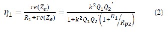
efficiency at the primary side, η1 .
At the secondary equivalent circuit, shown in Fig. 3 (b), the parasitic resistance can be converted into an equivalent parallel loss across the LC tank. The power from the primary part will be
dissipated in both R2 and RL , and the power consumed at RL
represents the net output power available at the receiver. At
![]()
resonance, the power efficiency at the secondary part, η2 can be written as
C. Maximum Power Transfer Efficiency
The power transfer efficiency can be maximized by adjusting
conditions such as R, L, C of coils and RL value. In practice, for planar integrated spiral inductors it is difficult to adjust the L, C, and R values of the coils independently, since all the values are
partially correlated. Therefore, R L is the best practical factor to adjust when optimizing the wireless link for a given coil. By
![]()
differentiating (4) w.r.t. RL, the optimal RL can be obtained as
![]()
This optimal condition makes the maximum power transfer efficiency a function of coupling coefficient k and quality factor of the coils, both of which may be optimized when designing the coils.
With large values of k and Q, the power efficiency approaches
1 as expected.
While high power transfer efficiency is critical for low power systems, area-constrained systems can require larger power transfer through smaller area coils at an acceptable loss in efficiency. With a fixed distance between two coils, larger coils result in larger k and higher efficiency. However, using larger coils requires more silicon area, and it ultimately decreases the power transfer density. Therefore, a parallel power transfer scheme can be taken into consideration in order to increase power density and maximize the amount of power delivery through the same area, as illustrated in Fig. 4.
IJSER © 2013 http://www.ijser.org
International Journal of Scientific & Engineering Research, Volume 4, Issue 10, October-2013 1059
ISSN 2229-5518

![]()
Fig. 5. Equivalent circuit for power density calculation
Fig. 4. Concept of parallel inductive power transfer (a) parallel power delivery using multiple maximum-power-density coils (b) single power delivery using one large coil
In order to compare the performance of single inductive power link to a parallel inductive power link, the power transfer density should be analyzed first.
A. Output Delivered Power
Fig. 5 shows that the transformer circuit has the equivalent circuit with reflected impedance and parallel resistance. The reflected impedance is split into the imaginary and real part, and the real resistive part is converted to parallel resistance
using quality factor ![]()
![]()
At resonance the input power is given by
and the output power can be written as
B. Optimal Load
The power transfer also can be maximized by adjusting the RL value. By differentiating (8) w.r.t.RL at resonance , the optimal RL can be expressed as
![]()
Substituting the optimal R L into (8), we get the maximum power transfer amount as
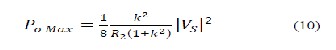
C. Power Transfer Density
![]()
The power transfer density is defined as the amount of available transferred power per the unit area. Assuming square- shaped, planar spiral coils are used with diameter d, the power transfer density will be a function of d. In addition, coupling coefficient k is also the function of d [9].
where x is the distance between coils. With (11), the power transfer density is given by
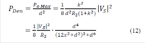
By differentiating (10) w.r.t. d, the optimal size of the coils and corresponding k can be found as the function of the separation between coils, x. For instance, when x=15μm, the optimal d is
58μm, and k is equal to 0.41.
A. Simulation Setup
To verify this model, we designed planar spiral coils using a Chartered 0.13µm CMOS process. Fig. 6 shows the simulation setup of two identical square coils vertically stacked to implement the inductive power link through stacked ICs. We sweep the separation x, and the diameter d to test power efficiency and density. HFSS is used to extract the lumped-element models for coils, and these models are imported to Sperctre to simulate the inductive power link.
B. Power Transfer Efficiency
As shown in (6), the maximum power transfer efficiency
IJSER © 2013 http://www.ijser.org
International Journal of Scientific & Engineering Research, Volume 4, Issue 10, October-2013 1060
ISSN 2229-5518
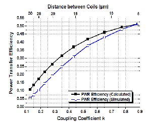
strongly depends on k. To show this dependency, we swept the distance x from 5µm to 30µm with 60µm-sized coils. It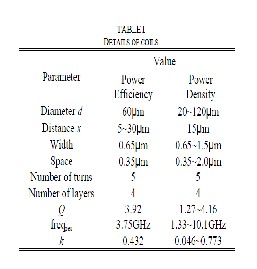
maintains a Q-factor of 3.9 while k varies from 0.125 to 0.887.
Fig.7. Coupling Coefficient k Vs. power transfer efficiency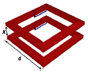
Fig .7 shows the simulation result of the maximum power transfer efficiency when using the optimal load resistance. The simulation values match the theoretical values well. As expected, higher k results in higher power transfer efficiency. When k=0.887(60µm coils, 5µm separation), we can achieve a power efficiency of 52%.
C. Power transfer Density
To verify the power density model, we designed 11 coupled
coils which have varying diameters from 20µm to 120µm in
10µm steps. The distance between the paired coils is fixed at
15µm, which can be reasonably achieved with face-to- face
stacking of two CMOS die. Over this range k varies from 0.05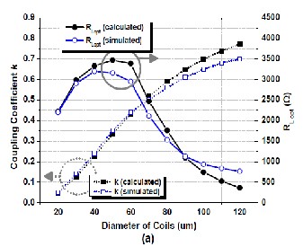
to 0.77, as shown in fig.8(a). While the specific dimensions, we can calculate k and optimal RL by (9) and (11) respectively, and the theoretical values match the simulation results.
Fig. 6. Two vertically stacked coils for wireless inductive power link
IJSER © 2013 http://www.ijser.org
International Journal of Scientific & Engineering Research, Volume 4, Issue 10, October-2013 1061
ISSN 2229-5518
efficiency and maximum power transfer for the three configurations shown in fig 9. Assuming the same area of
200µmX200µm , we assigned a 3x3 array of 60µmX60µm coils(optimal power density), a 2x2 array of 90µmX90µm, and a single 200µmX200µm (maximum power efficiency). The separation of the stacked coils is 15µm. The results are shown in fig 10. Since the single 200µm X200µm coil has the largest k, it has the highest power efficiency of 52%. However, the total delivered power amount becomes the largest with the 3X3 array because 60µmX60µm coil has the highest power density. A simulated power transfer of 1.48mW was achieved over the link, which is five times larger than the single inductive power link.
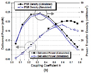
Fig. 8 (a) The coil diameter vs. coupling coefficient k and the optimal RL (b) Coupling coefficient k vs. power transfer amount and power transfer density
Fig 8(b) shows the maximum delivered power amount and power transfer density depending on k. As mentioned in section III , when the separation x= 15µm, the optimal coil size for the maximum power density is 58µm and k is 0.41. The simulation result verifies this; the optimal k is about 0.35 and the optimal size is about 55µm. The maximum power transfer density is 49mW/mm2.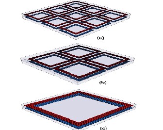
![]()
D. Performance Comparison
In order to compare the performance between parallel and single inductive power links, we simulated the power
The performance of a wireless inductive power link can be improved by using resonant inductive coupling. For low power systems and high power efficiency, higher k and Q are required. However, in order to increase the absolute power transfer amount, power density is critical and the optimal value of k to maximize power density depends on the distance and coil technology. Therefore, the parallel inductive power link with the optimal sized coils can deliver more power than the single inductive power link can while the latter has higher efficiency.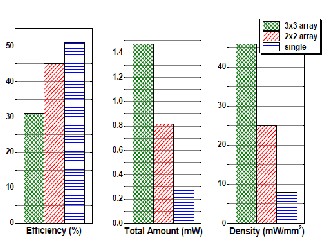
Fig.10. Simulation Results: power transfer efficiency, total delivered amount and power transfer density of three cases
VI. References
[1] K Niitsu, Y Shimazaki, Y Sugimori, Y Kohama, K Kasuga, I Nonomura M Saen, S Komatsu, K Osada, N Irie, T Hattori A Hasegawa and T Kuroda, "An Inductive- Coupling link for 3D Integration of a 90nm CMOS Processor and a 65nm CMOS SRAM," ISSCC Dig Tech. Papers 480-
481, Feb 2009.
[2] N. Miura, D Mizoguch i, T Sakur ai an d T Kor oda, “An alysis an d Design of luductrve Couphng and Transceiver
IJSER © 2013 http://www.ijser.org
International Journal of Scientific & Engineering Research, Volume 4, Issue 10, October-2013 1062
ISSN 2229-5518
Circuit for inductive interchip Wireless Superconnect”, IEEE Journal of Solid-State Circuits, Vol 40 pp 829-837, 2005.
[3] M. W. Baker and R. Sarpeshkar, “ Feedback Analysis and Design of RF Power links for Low-Power Bionic Systems; IEEE Trans Biomed. Circuits Syst” Vol 1, pp 28-38
2007.
[4] U Jow and M Chovanloo, “Design and Optimization of Printed Spiral Coils for Efficient Trauscutaneous Inductive Power Transnsmission”, IEEE Trans Biomed. Circuits Syst, Vol I, pp 193-202, 2007.
Canegallo, R_ Guerrieri, "Chip-to-Chip Commumcation Based on Capacitive., Coupling”, 'IEEE Conference on 3D system Integration 2009.
[6] Information Tethered Micro Automated Rotary Stages
(ITMARS), DARPR MTO BAA 08-74 [Online].
[7] A. Kurs, A. Karalis, R. Moffatt J D Joannopoulos, P Fisher, and M Solijacic, “Wrreless Power Transfer via Strongly Coupled Magnetic Resonances”, Science Express, Vol 317 no 5834, pp 83 - 86 July 2007.
[5] R Cardu, M Scanchiuzzo S Cani, L Perugini E Franchi, R
Akancha Srivastava Khare was born in Kanpur, Uttar Pradesh, India. She has received her B. Tech. degree in Electronics & Communication Engineering from Maharana Pratap Engineering College,Kanpur affiliated to Gautam Buddh Technical University Lucknow, Uttar Pradesh, India and persuing M. Tech. in Wireless Communication from Chandra Mohan Jha University Meghalaya, India. Currently she is a Asst. Professor in Maharana Pratap Engineering College Kanpur, Uttar Pradesh, India. Her area of interest Wireless Power Transmission.

Ashish Mishra was born in Etah, Uttar Pradesh, India. He has completed his B. tech. degree in Electronics & Communication Engineering from Saraswati Institute of Technology & Management, Unnao affiliated to Gautam Buddh Technical University Lucknow, Uttar Pradesh, India and persuing M. Tech. in Electronics & Communication Engineering from Gautam Buddh Technical University Lucknow, Uttar Pradesh, India. He is currently working as a Asst. Professor in Maharana Pratap Engineering College Kanpur, Uttar Pradesh, India. His are of interests
Wireless Communication and Image Compression.

Abhishek Kr. Mishra was born in Hardoi, Uttar Pradesh, India. He has received his B. Tech degree in
IJSER © 2013 http://www.ijser.org
International Journal of Scientific & Engineering Research, Volume 4, Issue 10, October-2013
ISSN 2229-5518
1063
Electronics & Communication Engineering from Bhabha Institute of Technology Kanpur Affiliated to Gautam Buddh Technical University Lucknow, Uttar Pradesh, India with flying color marks. He is currently persuing M.Tech. in Electronics & Communication Engineering from Gautam Buddh Technical University Lucknow, Uttar Pradesh, India. His area of interests VLSI System Design, Image Compression and Wireless Communication. He guided many projects forB Tech Students.