International Journal of Scientific & Engineering Research, Volume 3, Issue 11, November-2012 1
ISSN 2229-5518
WiMax PLL's FIR Filter Design Using LMIs
Hatem Elaydi, Ayman Alquqa, H Khozondar
Abstract—WiMax technology evolved greatly over the last decade. Using optimization techniques to improve the behavior of filters in phase-locked loop (PLL) in terms of overshoot and setlling time is a challenging task. This paper introduces a new PLL's loop filter design methodology that meets mobile WiMax design objectives such as small settling time, minimum overshoot and working mobile WiMax frequency range. LMI optimization based on semidefinite programmimg is used for FIR filter design to optimize conflicting objectives. The obtained results are compared with linear programming results. The LMI results outperformed results of linear programming and other comparable designs.
Index Terms— LMI, PLL, FIR, Mobile WiMax, Frequency Synthesizer
—————————— ——————————
1. INTRODUCTION
he fourth generation (4G) of mobile broadband networks is based on the foundation of worldwide Interoperability for Microwave Access (WiMax)[1]. Quality of Service
(QoS) for different traffic classes, robust security, and mobility are guaranteed by WiMax. The phase-locked loop (PLL) is basically an electronic circuit that maintains a constant phase angle relative to a reference signal by controlling an oscillator [2]; moreover, it plays a significant part in WiMax system. PLLs are most commonly used in frequency synthesizers of wireless systems. A frequency synthesizer generates a range of output frequencies from a single stable reference frequency of a crystal oscillator [3]. In communication systems, many appli- cations require a range of frequencies or a multiplication of a periodic signal. For example, in most FM radios, a PLL fre- quency synthesizer is used to generate 101 different frequen- cies. In order to generate highly accurate frequencies with varying precisely steps, such as from 600 MHz to 800 MHz in steps of 200 KHz, most wireless transceiver designs employ a frequency synthesizer. Frequency Synthesizers are also widely used in signal generators and in instrumentation systems, such as spectrum analyzers and modulation analyzers. A basic configuration of a frequency synthesizer is shown in Figure 1.
The basic frequency synthesizer includes a very stable crystal oscillator and N- programmable divider in the feedback loop in addition to the PLL. The programmable divider divides the output of the Voltage Controlled Oscillator (VCO) by N and locks to the reference frequency generated by a crystal oscillator.
The output frequency of VCO is a function of the control voltage generated by the phase detector/comparator (PD). The output of the phase comparator, is proportional to the phase difference between the signals applied at its two inputs, controls the frequency of the VCO. Thus, the phase comparator input from the VCO through the programmable divider remains in phase with the reference input of crystal oscillator. Therefore, the VCO frequency is maintained at  . This relation can be expressed as
 (1)
(1)
where fr is fractional frequency and N is an integer number.
This implies that the output frequency, f0 is equal to
 (2)
(2)
Using this technique, a number of frequencies separated by
 and a multiple of N can be produced. For example, if the

fr
Phase
Detector
Loop
Filter
Programmable
Counter ( )
fo
VCO
input frequency is 24 KHz and the N is 32, then the output frequency is 0.768MHz. In the same manner, if N is an array of numbers, then the output frequencies will be a proportional array. This basic technique form using phase locked loop technique is used to develop a frequency synthesizer using a single reference frequency. As for the phase detector in Figure

1, represents the phase input,  the phase error, and output phase. Phase error (phase detector output) can be
Fig. 1. Basic Frequency Synthesizer
calculated such as
————————————————
Hatem Elaydi is currently working as a professor in electrical engineering Department at the Islamic University of Gaza, Palestine. E-mail: helaydi@iugaza.edu.ps
Ayman Alquqa is holding a masters degree in electrical engineering from the Islamic University of Gaza, Palestine. E-mail: aalqouqa@gmail.com
and the VCO output can be calculated such as
(3)
(4)
Hala Khozodar is currently working as a professor in electrical engineering Department at the Islamic University of Gaza, Palestine. E-mail: hkhozon- dar@iugaza.edu.ps
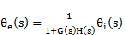
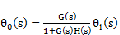
where  is the feedforward transfer functions, and
  is the feedback transfer functions [3].
IJSER © 2012
http://www.ijser.org
International Journal of Scientific & Engineering Research, Volume 3, Issue 11, November-2012 2
ISSN 2229-5518
The loop filter performs the filtering operation of the error voltage (coming out from the Phase Detector). The output of phase detector consists of a dc component superimposed on an ac component. The ac part is an undesired input signal to the VCO; hence, a low pass filter is used to filter out the ac component. The loop filter is an essentional functional block in determining the performance of the loop. In addition, a loop filter introduces poles to the PLL transfer function, which plays key role in determining the bandwidth of the PLL. Since higher order loop filters offer better noise cancelation, a loop filter of order 2 or more is used in most of the critical application PLL circuits.
One desirable property of all PLLs is that the reference and
Ref
20MHz
PFD Loop
Filter
76 - 90
Div-N
Div-2
1533-1800MHz
VCO
Fout
2300-2700MHz
feedback clock edges be brought into very close alignment [4]. The average difference in time between the phases of the two signals when the PLL has achieved lock is called the static phase offset (the steady-state phase error). The variance between these phases is called tracking jitter. Ideally, the static phase offset should be zero, and the tracking jitter should be as low as possible.
Phase noise is another type of jitter observed in PLLs [4],
and is caused by the oscillator itself and by elements used in
the oscillator's frequency control circuit. To keep phase noise low in PLL circuits, it is best to avoid saturating logic families such as transistor-transistor logic (TTL) or CMOS.
The main contribution of this paper is designing a specified PLL loop filter that works properly and efficiently with Mobile WiMax system. Selecting the filter's coefficients is based on LMIs using semidefinite programming (SDP) optimization techniques that are compatible with Mobile WiMax system. The designed loop filter must be stable and meet the following specifications: Frequency range (2.3 – 2.7) GHz used for Mobile WiMax systems, small settling time to lower the lock- in range and a very small overshoot.
Traditional frequency synthesizers use low-pass analog
filter to eliminate the high frequency components, but in this paper we use FIR digital low-pass filter to eliminate the high frequency components in order to improve noise immunity. N-Fractional Synthesizer is used instead of N-Integer Synthesizer to reduce noise resulted from the factor N.
This paper is organized as follows: Section 2 covers methodology used to design and optimize PLL loop filter. FIR low-pass digital filter using LP and LMI methods is introduced in section 3. Section 4 shows the results and discussions of LP and LMI designs. Conclusion and future work are outlined in section 5.
2. METHODOLOGY
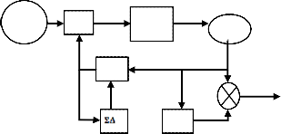
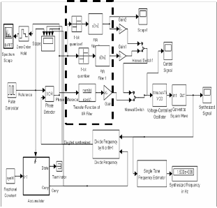
The fractional-N PLL block diagram shown in Figure 2 consists of:
Phase/Frequency detector which is assumed XOR
type.
Loop Filter which is the objective of our design which
is a Low-pass filter (LPF).
Voltage Control Oscillator (VCO).
Fig. 2. Fractional-N PLL block diagram
We started by designing an Integer-N PLL: 125 KHz reference pushes N from 18400 to 21600 (2700/.125). The resulted loop filter cutoff (<12.5 KHz) produced big settling time and the VCO phase noise increased by  To overcome the previous drawback, we used Multi-
Modulus Fractional PLL with the following specifications:
Fractional value between N and 2N-1 (64-127).
Sigma Delta Modulator (Programmable resolution).
Large Reference (20MHz) for good tradeoff with settling time.
Reduced N impact on phase noise by 45dB over
Integer N.
Example 1: To obtain 2300MHz frequency, we produced
1533MHz (from VCO) and then upconvert it to 2300MHz (1533MHz * 1.5 ≈ 2300MHz). The 1533MHz can be produced with N = 76 and a fraction = 0.65 (means that 20MHz * (76 +
0.65) = 1533MHz).
As a result, for N = (76 ~ 90), it can produce frequency range (1533MHz ~ 1800MHz), which can be upconverted to (2300MHz ~ 2700MHz).
Figure 2 shows the Fractional-N PLL design block diagram, with N range from 76 to 90 and  is the fraction. Our goal now is to design digital FIR low pass loop filter in order to meet the previously mentioned requirements. The design will be encouraged by two different optimization methods, Linear programming (LP) and Semi-Definite programming (SDP).
3. FIR LOW-PASS FILTER DESIGN
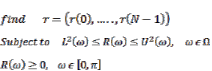
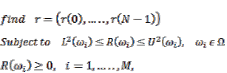
We consider the problem of designing a finite impulse response (FIR) filter with upper and lower bounds on its frequency response magnitude [5]: given filter length N, find
filter tap coefficients , such that the frequency response satifies the
magnitude bounds
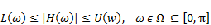
(5)
IJSER © 2012
http://www.ijser.org
International Journal of Scientific & Engineering Research, Volume 3, Issue 11, November-2012 3
ISSN 2229-5518
over the frequency range  of interest.

One conventional approach to FIR filter design is Chebychev approximation of a desired filter response , i.e., one minimizes the maximum approximation error over .
We present a new way of solving the proposed class of FIR

filter design problems, based on magnitude design i.e., instead
of designing the frequency response of the filter directly, we design its power spectrum to satisfy the magnitude bounds [5].
Let autocorrelation function  denote
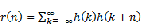 (6)
(6)
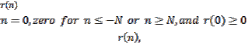
where we take  . The sequence is symmetric around
. Note that the
Fourier transform of
 (7)
(7)
is the power spectrum of  . If we use r as our design variables, we can reformulate the FIR design problem in RN as
 (8)
(8)

The non-negativity constraint is a necessary and sufficient condition for the existence of satisfying (6) by the
Fejér-Riesz theorem (see § 4 in [5]). Once a solution of (7) is
found, an FIR filter can be obtained via spectral factorization. An efficient method of minimum-phase spectral factorization is given in Section 4 in [5].
3.1 LP formulation
A common practice of relaxing the semi-definite program (7) is to solve a discretized version of it, i.e., impose the constraints only on a finite subset of the [0, ] interval and the problem becomes
 (9)
(9)
where  . Since
  is a linear function in r for each i, (8) is in fact a linear programming problem that can be efficiently solved. When M is sufficiently large, the LP formulation gives very good approximations of (7). A rule of thumb of choosing M,
  , is recommended in [6]. According to that we assumed M = 15N along this paper.
3.2 LMI formulation
We will show that the non-negativity of  for all
  can be cast as an LMI [7] constraint and imposed exactly at the cost of
  auxiliary variables. We will use the following theorem.
Theorem 1 Given a discrete-time linear system  , A
, A
stable, minimal and  . The transfer function satisfies
 (10)
(10)
if and only if there exists real symmetric matrix P such that the matrix inequality
 (11)
(11)
is satisfied. Detailed proof of this theorem can be found in
[5].
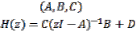
In order to apply Theorem 1, we would like to define H(z) as deadbeat system where H(z) is defined as a rational function with its denumerator consists of one term with z to the power of N. Then, this system is represented in delay mode, z-1, which leads to a polynomial with N coefficients stored in array r. Thus,
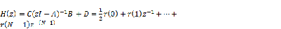
 is defined such as
(12) An obvious choice is the controllability canonical form:
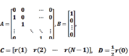 (13)
(13)

It can be easily checked that  given by (11) satisfies (10) and all the hypotheses of Theorem 1. Therefore the existence of
  and symmetric that satisfy the matrix inequality (9) is the necessary and sufficient condition for
  by Theorem 1.
Note that (9) depends affinely on  and
and  . Thus we can
formulate the SDP feasibility problem:
IJSER © 2012
http://www.ijser.org
International Journal of Scientific & Engineering Research, Volume 3, Issue 11, November-2012 4
ISSN 2229-5518
 (14)
(14)

with  given by (11). The SDP feasibility problem (12)
can be cast as an ordinary SDP and solved efficiently.
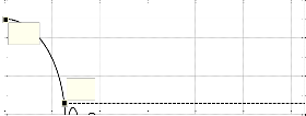
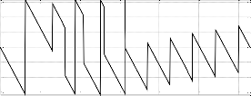
The simulation model produced synthesized frequency in the range of (1.533GHz – 1.8GHz) that must be multiplied by
1.5 to obtain the required range (2.3GHz – 2.7GHz).
4.1 LP (Linear programming)
The FIR filter design is obtained using LP as shown in
Figure 4.
10
4. RESULTS AND DISCUSSIONS
In order to perform simulation for the designed filters, a simulation module as shown in Figure 3 is built using MATLAB and Simulink.
Filter Bank
0
-10
-20
-30
-40
-50
3
2
1
0
-1
-2
-3
X: 0.01885
Y: -0.4
X: 0.6283
Y: -44.5
0 0.5 1 1.5 2 2.5 3 w
0 0.5 1 1.5 2 2.5 3 w
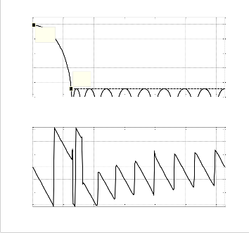
Fig. 3. Magnitude/Phase Response (LP)
Fig. 2. PLL Frequency Synthesizer Simulation Model
The FIR filters parameters are obtained using the MATLAB convex optimization toolbox, CVX [8]. The simulation module consists of:
Reference Frequency: Pulse generator is chosen to produce 20MHz.
Filter Bank: two filters are designed and separated by
Figure 4 shows the designed FIR filter length of 21 taps where filter order equals to 20. Figure 4 shows that:
The maximum passband ripple does not exceed 0.4 dB
with  .
.
Stopband attenuation is below -44.5 dB with
 .
.
The simulation results of the Mobile WiMax for this FIR
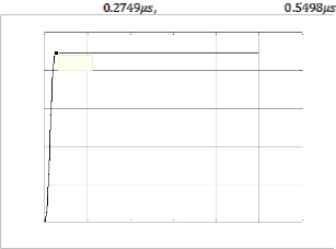
filter produced the correct and proper output frequency as shown in Figure 3. The simulation result of the control signal using this FIR filter as shown in Figure 5 produced: zero overshoot, rise time of and settling time of .
2.5
X: 5.498e -007
Y: 2.223
manual switch as shown in Figure 3.
Voltage Controlled Oscillator (VCO) with output
signal amplitude equal to 1V, quiescent frequency equal to 1.511 GHz, and input sensitivity equal to
10MHz/V.
Phase Detector: XOR type selected.
Frequency Divider which produces (synN + synM) values used to divide the output of VCO. Where synN is the integer and synM is the fraction.
2
1.5
1
0.5
0
0 0.2 0.4 0.6 0.8 1 1.2
Sigma/Delta Modulator: to produce the required
Time (s)
-5
x 10
fraction synM.
The Gain formula , where
 after the output of FIR filter.
Fig. 4. Control Signal of VCO input using Designed FIR Filter
4.2 LMI
The second FIR filter design is obtained using SDP as shown in Figure 6.
IJSER © 2012
http://www.ijser.org
International Journal of Scientific & Engineering Research, Volume 3, Issue 11, November-2012 5
I
0
-10
-20
-30
-40
-50
X: 0.01885
Y: -0.4
X: 0.6283
Y: -44.5
0 0.5 1 1.5 2 2.5 3 w
using SDP outperformed other techniques regarding filter order, settling time and overshoot.
TABLE 1
COMPARISON BETWEEN PROPOSED FIR DIGITAL FILTER DESIGNS AND OTHER DESIGNS


3
2
1 


0 


-1
-2
-3
0 0.5 1 1.5 2 2.5 3 w
Fig. 5. FIR Filter Magnitude/Phase Response (SDP)
Figure 6 shows a 19 taps FIR filter with filter order of 18 (fewer than LP FIR length). Figure 6 shows that:
The maximum passband ripple does not exceed 0.4 dB
with  .
.

Stopband attenuation is below -44.5 dB with
.
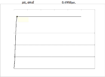
The simulation results of Mobile WiMax as shown in Figure 3 worked properly and produced the correct output frequency. The simulation results of the control signal using this FIR filter as shown in Figure 7 produced: zero overshoot, rise time of 0.25 settling time of
2.5
X: 4.998e -007
2 Y: 2.194
5. CONCLUSION AND FUTURE WORK
Optimal design of phase-locked loop in WiMax technology can improve system behavior (overshoot & settling time). A new loop filter design method for frequency synthesizer is used in mobile WiMax. The proposed method took into consideration various design objectives such as: small settling time, minimum overshoot and mobile WiMax frequency range. FIR digital low pass filter was designed using linear programming and LMI optimization based on semidefinite programming. Simulations results showed that FIR lowpass digital filter utilizing linear programming and semidefinite programming improved the transient behavior. The simulated results also showed that the filter met the Mobile WiMax systems working frequency range of (2.300 GHz – 2.700 GHz) and has the power to include much higher frequency bands. The designed method of LMI optimization using Semidefinite programming outperformed the LP filter design and did much better than similar work by others.
Further research can concentrate more on VCO noise and
optimizing filter order.
1.5
1
0.5
0
0 0.2 0.4 0.6 0.8 1 1.2
REFERENCES
[1] WiMax Forum, http://www.wimaxforum.org/home, accessed Feb
2012.
[2] Gorry Fairhurst, Physical Layer, Communication Engineering Course, School of Engineering, University of Aberdeen, UK, accessed Sep. 2012. http://www.erg.abdn.ac.uk/~gorry/course/docs/phy.pdf.
Time (s)
-5
x 10
[3] R E Best, Phase-Locked Loops: Design, Simulation, and Applications, Sixth
Fig.7. Control Signal of VCO input using Designed FIR Filter (SDP)
The filter design using SDP technique outperformed LP technique with reduced filter length of 19 taps instead of 21 taps, lower settling time and lower rise time. Moreover, the proposed SDP filter design also outperformed filter designs by Chou's [9], Staggs' [10] and Kozak's [11] in terms of settling time and overshoot as shown in Table 1. Unfortunately, the rise time did not meet Chou's and Staggs' results. Filter design
Edition. New York: McGraw Hill International (2007).
[4] Wikimedia Foundation, Phase Locked Loop, Wikiperia. Oct. 2012, accessed Oct. 2, 2012. http://en.wikipedia.org/wiki/Phase- locked_loop.
[5] S P Wu, S Boyd and L Vandenberghe, “FIR filter design via semidefi- nite programming and spectral factorization,” the 35th IEEE Decision and Control conference, pp. 271-276, 1996.
[6] A Alkhairy, K Christian, and J Lim, “Design of FIR filters by complex
Chebyshev approximation,” Proceedings of the Acoustics, Speech, and Sig- nal Processing, Washington, DC, USA, 1991, pp. 1985 – 1988, 1991.
IJSER © 2012
http://www.ijser.org
International Journal of Scientific & Engineering Research, Volume 3, Issue 11, November-2012 6
ISSN 2229-5518
[7] S Boyd, L El Ghaoui, E Feron, and V Balakrishnan, Linear Matrix Ine- qualities in System and Control Theory, Philadelphia: SIAM, 1994.
[8] CVX: Matlab software for disciplined convex programming: vesion 2.0, Sep. 2012, accessed Oct. 6, 2012. http://cvxr.com/cvx.
[9] Y Chou, W Mao, Y Chen, and F Chang, F. “A novel loop filter design
for phase-locked loops,” the International IEEE Conference on Systems, pp. 2932 – 2938, 2006.
[10] E Staggs, “Mobile Wi-Max radio: phase locked loop design,” Converage: an application for high-performance design workshop, ANSOFT Corp, ac- cesed Sep. 28, 2012. http://www.ansoft.com/converge/staggs_ansoft.pdf.
[11] M Kozak, and E Friedman, “Design and simulation of fractional-N
PLL frequency synthesizers,” Proceedings of the 2004 International Sym- posium on Circuits and Systems, pp. IV- 780-3, 2004.
IJSER © 2012
http://www.ijser.org