International Journal of Scientific & Engineering Research, Volume 4, Issue 12, December-2013
ISSN 2229-5518
24
Transient Time Slot (TTS) based Run Time Leakage Reduction Method for Low Power VLSI Circuits
V.S.V.Prabhakar1, K.Lal Kishore2
Abstract- Due to Technology scaling the importance of leakage power has significantly increased in the modern day system-on-chip devices. The runtime leakage component during the active state is almost becoming equal to the standby leakage component. Hence Present day research is more focused on reduction of runtime leakage current .we present a novel runtime leakage reduction for 70nm technology. As an attempt to save the leakage power in the active mode, run-time power gating is explored at various design levels. In the present work we propose a power control method based on Transient Time Slot (TTS) of a logic gate. Using static timing analysis, for each logic gate of the circuit we find its idle period (non-transition period) within the clock period. W e switch off the power supply during that period which saves significant amount of run time leakage power. The Logic gates are partitioned according to a heuristic algorithm proposed into clusters so that pair of control transistors is attached to each cluster. Power is supplied only during Transient Time Slot. W e simulated ISCAC’85 bench mark circuits and observed that there is significant amount of run time leakage saved. W e designed a multiplier using the proposed approach and observed about 85% of runtime leakage savings. Later we simulated c6288 netlist which is a ideal transistor netlist and observed that same amount of runtime leakage power is saved as that of TTS method. There is slight increase in the area and delay which is trade off with the leakage savings
Index Terms—Runtime leakage, Transient Time Slot, Optimization function, Partitioning algorithm.
1. INTRODUCTION
—————————— ——————————
IJSErun-time powRer gating is explored at various design levels.
Power gating techniques that have been developed so far
mainly aim at reducing leakage current at the standby
mode. However, the requirement for leakage reduction is extending to the active mode. This is because leakage power dissipation increases exponentially with device scaling and is projected to exceed dynamic power dissipation below
65nm feature size [1]. This means that leakage current
becomes the major contribution to power dissipation in the active mode. As an attempt to save the leakage power in the active mode,
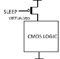
Figure 1: Traditional power gating Technique

• V.S.V.Prabhakar is working as Professor in the Dept of ECE at Gayatri Vidya Parishad College of Engineering for Women, Vishakapatnam India.
E-mail: prabhakarvsv@gmail.com
• Prof (Dr) K.Lal Kishore is Professor in ECE and
Vice-Chancellor of JNTU Anantapur India. E-mail: lalkishorek@yahoo.com
In the present work we propose a power control method
based on Transient Time Slot (TTS) of a logic gate. Using
static timing analysis, for each logic gate of the circuit we find its idle period (non-transition period) within the clock period. We switch off the power supply during that period which saves significant amount of run time leakage power. In this paper, we first discuss the basic concept of TTS based technique, a heuristic based dynamic programming based algorithm to partition the circuit, later its implementation through a series of simulations and finally discuss the leakage savings.
2. POWER GATING METHODOLOGIES
Power gating technologies were initially used to reduce standby leakage reduction. A low Vth sleep transistor was inserted between the power and the CMOS logic (Fig 1). When the logic is not active a sleep signal is given as input to the sleep transistor so that it shutdowns the power supply to the logic. Because of the stacking effect the subthreshold leakage current dramatically reduced. As there is voltage drop across the gate oxides because of virtual VDD , gate leakage current also reduced. But there is significant domination of overall leakage power on subthreshold leakage and gate leakage hence this approach is not suitable for smaller technologies.
IJSER © 2013 http://www.ijser.org
International Journal of Scientific & Engineering Research, Volume 4, Issue 12, December-2013
ISSN 2229-5518
25
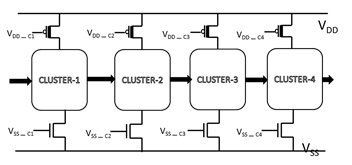
Figure 2: Architecture of proposed TTS Method
There is additional delay contributed by 6 % using traditional power gating Technologies. So the delay contributed is also serious issue. Hence the existing power gating methodologies should be modified to achieve runtime leakage savings.
3. BASIC IDEA OF TTS BASED METHOD
When the digital circuit is in operating mode, each logic gate
supply to all the gates in the particular cluster are controlled by a pair of NMOS and
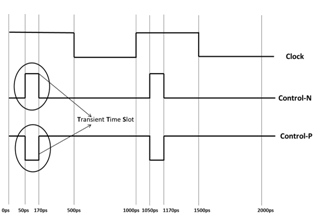
Figure 3: Concept of TTS shown along with wave forms of control signals
PMOS transistors (also known as control transistors) as discussed above. For each cluster two control signals are
IJSER
within it will not undergo transition throughout the time
period of the clock. It switches to a particular logic within small interval of time slot of the clock period. This time slot should be definitely less than the clock period and is known as “Transient Time Slot (TTS)”. The basic idea of the proposed technique is if power is supplied to the logic gate only for Transient Time Slot (TTS), significant amount of runtime leakage power can be saved. There is small amount of delay introduced with this technique which is a tradeoff, as the amount of runtime leakage current is more compared to the standby leakage current for smaller dimensions[1].This method is verified on 65 nm transistor technology logic gates which will be discussed in the coming topics and can be extended to sub-70nm also. The switch-off time is the difference of total clock period and TTS. Fig 2 gives the architectural diagram for the proposed technique. In the proposed architecture we need both NMOS and PMOS transistors used to cut-off the power supply when the logic gate is not in transition state. The reason is when the output of the CMOS gate is high, there is conduction path through Pull-up network and Leakage path exists through Pull-Down network. The same argument is valid when the output is low. Hence two types of transistors are needed. The digital circuit is divided into cluster’s whereas cluster is group of logic gates with same Transient Time Slot (TTS). Though there is no guarantee that many transistors have same Transient Time Slot (TTS), we round- off to the nearest Picoseconds which shall be discussed in detail in the coming sections of the chapter. The power
generated by control circuitry and given as inputs to the
Control transistors. They are shown as VDD_Ci and VSS-Ci in
the Figure 2. The control circuit operates at global clock frequency of the circuit. As the Transient Time Slot (TTS) of each cluster is same, the control signals are so tuned that they switch-on the control transistors only during that time. For example let us consider a Clock of 1 GHZ frequency. Figure 3 shows the relation between clock period and control signals which control a cluster with TTS is (50ps,
170ps) for a period of 120ps.Though the clock period is as
wider as 1000ps, the control signals are active only during [50ps, 170ps] in the first cycle and during [1050ps, 1170ps] in the second cycle. During each clock cycle we can switch-off power for 880ps as the transition of the cluster takes place only for 120ps time.Likely we can save significant runtime leakage power for a digital circuit
4. STEPS TO IMPLEMENT TTS METHOD.
We extended the above idea to be implemented in four steps to reduce the unnecessary cost and size of the circuit.
Step 1: Calculation of Minimal Transient Time Slot (MTTS)
of each logic gate.
Step 2: Partition of the circuit based on heuristic algorithm.
Step 3: Insertion of Control transistors and generation of control signals.
Step 4: Verification of circuit for power savings through simulation.
IJSER © 2013 http://www.ijser.org
International Journal of Scientific & Engineering Research, Volume 4, Issue 12, December-2013
ISSN 2229-5518
26
5 CONCEPT AND IMPLEMENTATION OF TTS BASED LEAKAGE REDUCTION METHOD
5.1 Concept of Transient Time Slot (TTS)
The concepts of Transient Time Slot and Minimal Transient Time Slot (MTTS) for a logic gate are derived from method of [2]. In the Figure 4 we consider a CMOS logic gate, with n-inputs and a single output. For a node in the circuit, a time slot (x, y) can be defined with two variables. x is the time when a particular signal arrives at the earliest and y is the time when the signal arrives lately. At any point of time the signal must arrive within this time slot (x, y) and transition takes place. For the CMOS logic gate with n-inputs considered, delay exists which effects the time slot of the output. Various factors like ON resistance of the transistor and Load capacitance (CL ) contribute for the delay. Let the smallest delay of the gate is Dmin and largest is Dmax. As there are n- inputs and each one has its own time slot the input time slot, ranges from (x1 ,y1 ) ,(x2 ,y2 ) to (xn ,yn ) where as output time slot is (xo ,yo ). The relation between output
time slot and input time slot is given by
leakage power reduction and delay. The dynamic power saved per logic gate (Pdyn ) is given by
P α=. Toff (2)
dyn T
Where Pdyn is leakage power savings per gate,Toff is time period for which power is cut off,T is time period of the clock,α is constant that determines the efficiency whose value lies between the 0< α<1. It is obvious that significant leakage power savings were observed when at least 33% of the clock period time is Toff period. The value is quite less than expected (at least 50%) because the control transistors will take some time to switch-off which further delays

Figure 4: A CMOS logic gate with input and output time slots
IJSER
yo = max [yi +Dmax ]
x o = min [xi +Dmin ] (1)
If the delay of each logic gate is known along with the time slot of the primary inputs, using Eq 1 we can calculate time slots of all nodes of the circuit between Primary inputs (PI) and Primary outputs (PO). The maximum yo of all primary outputs is the worst-case delay of the circuit called as critical path. In general the maximum path delay of the circuit determines the clock period so that all operations are completed within the clock cycle. In real time 15% to 20 % extra time is added to the clock cycle in the design phase for any extra delays. The TTS of a logic gate is defined from the time slot method. Transient Time Slot (TTS) is defined as [min [xi], yo ] where min [xi] is the earliest arrival time among all inputs and yo is the latest time of output availability. During each clock cycle the logic gate is active only within this time (TTS) during which all switching operations take place while for rest of the clock period it remains inactive. The basic idea of the proposed technique is to supply power to the logic gate only during Transient Time Slot (TTS) time without affecting the transitions and power-off during the remaining time. This approach not only reduces the dynamic power consumption but also active leakage power. There is slight penalty on the delay of the circuit which can be considered as a tradeoff between
switching off of virtual power supplies (Virtual VDD and Virtual VSS shown in Figure 2). If the inputs to the logic gate come from different paths within the circuit then different inputs have different time slots.If there is large difference among the Time slots, the Transient Time Slot (TTS) becomes very wider. The wider Transient TTS of a particular logic gate makes Transient Time Slot (TTS) of its fan-out gates even much wider. This process continues until TTS becomes comparable to the worst case delay of the circuit. This will not help us to save leakage power as we never switched off the power during the clock cycle.
5.2 Minimal Transient Time Slot (MTTS)
Minimal Transient Time Slot (MTTS) of a logic gate is defined as minimum time slot during which we turn on the power supply without affecting the longest delay and the functionality. It is calculated as ((yo -Dmax), yo ) in which yo is the latest arrival of the output signal and Dmax is the maximum delay of the logic gate. In true sense there is no need to turn on the gate before all signals arrives. If we turn on the gate Dmax units earlier we can ensure that the output is obtained before or at yo. The longest delay of the circuit is dependent on yo but not on xo .When we switch on the power during ((yo -Dmax), yo ), the worst case longest delay is not violated and functionality is also ensured. Though the control transistors introduce extra delay it is uniform as similar transistors are used for each cluster. The width of TTS is dependent on maximum delay of the gate, which is
IJSER © 2013 http://www.ijser.org
International Journal of Scientific & Engineering Research, Volume 4, Issue 12, December-2013
ISSN 2229-5518
27
very less compared to the worst delay in the larger CMOS
circuits. The unbalanced gate delays and delay differences of the input signals will not affect the Minimal Transient Time Slot (MTTS).The power is supplied to gate only within its MTTS so that significant amount of runtime leakage can be saved. In this approach we do not turn on the power until all the inputs are stabilized which avoids unnecessary spiky transitions leading to glitches thus saving dynamic power. We used 70 nm CMOS BPT models for simulation. Each CMOS gate is modeled as RC network to calculate delay [3].Using the parameters and equations of BSIM3 model, CL value of the gate is calculated. Equivalent Resistance R of the Pull-up and Pull-down network is calculated depending on the type of the gate, fan-in, fan-out and transistor sizes. The delay calculations of the logic gates are applied to ISCASˊ85 benchmark circuits. There is deviation of 10% between calculated values of BSIM3 models and CADENCE SPECTRE simulations done on the same benchmark circuits. Once the worst case delay of logic gate is obtained Minimal Transient Time Slot (MTTS) can be
calculated using ((yo -Dmax), yo ).The value of yo is calculated
reduced with the partition of the circuit. The basic idea of
partition algorithm is few TTSˊs can be combined to form a cluster with negligible effect on the leakage savings. The Transient Time Slot (TTS) of the cluster is union of all TTS’s of all logical gates in it.For a cluster with n logic gates with TTS’s ranging from (x1 ,y1) ,(x2 ,y2 )……. (xn ,yn ), the TTS for the entire cluster is (max(xi),max(yi)) whereas i=1,2,3…..n. To partition the circuit an algorithm is proposed using greedy approach and based on dynamic programming to optimize the leakage savings and hardware cost. Here the cost is the parameter which represents additional hardware (control transistors) and delay contributed by them. The optimization function OF is defined as
OF =β .1L -Sβ .2CF (3) Where LS is percentage of total active leakage power to be saved using the current partitioning algorithm, CF cost function which is the parameter for estimation of total area and delay cost for the proposed partitioning method, β1 , β2 are weights of LS and CF. As β1= 1-β2 , substituting in Eq 3
we obtain
using static timing analysis.As there is 10% deviation is possible in delay calculations, the MTTS size is slightly
increased as ((yo -Dmax)-Dmax/2,yo +Dmax/2) i.e is it is
OF =(1β-
)2.L -Sβ .2CF (4)
purposefully increased by 2 times. The MTW width is very
smaller compared to the clock period hence increasing its
width will not show its significant effect on the leakage savings.
5.3 Partition of the circuit based on heuristic algorithm.
β2 sets the relative weights of LS and COST. By adjusting the
value of β2 we can optimize the circuit for more leakage
savings and reasonable increase in delay and area. The CF function is related to the number of clusters and TTS of each cluster. Cost function CF is defined as
Nclsuters W
CF= ∑ C_CF. K
(5)
An integrated circuit consists of hundreds and thousands of
logic gates and each logic gate has its TTS.A cluster is a group of logic gates of the circuit with same TTS. As discussed earlier the entire circuit should be partitioned into clusters. Dynamic programming based on heuristic algorithmic approach is used for partitioning the circuit. Before implementing the Partition algorithm there might be some logic gates with same TTS and so that they are grouped under the same cluster. But the number of such clusters will be more and each cluster needs a pair of control transistors attached to it which increases lot of extra area. For example for the circuit c880 (Table 4) in ISCAS’85
Benchmark circuit the total number of gates in it is 360 and
before partitioning there are 212 clusters with 1.7 gates per each cluster. With so many clusters the hardware of the circuit considerably increases which again shows its impact by increase in delay. But after implementing the partition algorithm the number of clusters reduced to 15 with average
24 per cluster. Hence the cost of hardware has considerably
k=1 T
Nclusters is the number of clusters of the entire circuit, C_CF is overall cost of the cluster per unit time of TTS, WK is width of the Transient Window of a particular cluster and T is time
β2 | Leakage savings(Estimated) | CF |
0.34 | 84.6% | 17.5% |
0.51 | 82.8% | 15.1% |
0.62 | 81.9% | 13.7% |
0.69 | 81.4% | 12.6% |
0.72 | 75.3% | 12.1% |
0.75 | 78.4% | 12.3% |
0.80 | 77.1% | 11.9% |
Table 1 Estimated leakage savings and cost (CF) versus β 2
period. We set the values of C_CF = 0.1 and β2 =0.69 in the calculations because these values give 80% of leakage
IJSER © 2013 http://www.ijser.org
International Journal of Scientific & Engineering Research, Volume 4, Issue 12, December-2013
ISSN 2229-5518
28
savings with less than 13% of CF. Table 1 gives leakage
savings estimated and cost function CF under different values of under different β2 values when C_CF = 0. When the value of β2 is increasing the estimated average leakage savings reduced with simultaneous reduction of cost CF, hence a reasonable value of β2 =0.69 is set. We assume the same amount of leakage for all the gates in the circuit to make the calculation easy. The total leakage savings is given by
NG (T-W )

S
TTS’s. If there are no TTS between two TTS’s we say they
are nearer. Basing on the above observation we combine only those Transient Time Slot’s which are nearer on the time scale. Suppose there are NMTTS initially. When we combine the nearby clusters the number of possible partition schemes P(NMTTS ) reduces to.
P ( NMTTS ) = 1 + P (1) P ( NMTTS − 1) + P (2) P ( NMTTS -2) + P (3) P ( NMTTS − 3) +…….
+ P ( NMTTS − 2) P (2) + P ( NMTTS − 1) P (1) - NMTTS − 2
Where P(K) represents the total number of clusters possible in the Logic circuit with K time slots when we combine the
L =λ. K
K=1 T
(6)
nearby TTS’s.Suppose K=2 P(2) =1+P(1)P(1) that means
NG is total number of gates in the circuit and WK is width of
the Transient Window of a particular cluster and T is time
period while λ is parameter for estimation of leakage
savings. λ is obtained by comparing the estimated leakage savings and average leakage savings from NanoSim simulations. A good value of λ that is closer to simulations is 0.968. We observe that λ is closer to 1 because the ratio Toff/ T from Eq 2 is very small which supports that switching
activity takes only very small slot of the total clock period.
either 1 cluster is possible or two clusters with one TTS each is possible. Similarly if k=3 ,P(3)= 1+ P(1)P(2)+ P(2)P(1)+P(3) which means if there are three TTS’s they can be partitioned into either into one cluster with all TTS’s combined or 2 clusters( one TTS’s and two TTS’s) or we cannot partition them (P(3)). For any number of partitions Eq 8 can be applied. Even after combining the nearby clusters the search space is very wide. Hence Dynamic Programming is used to
reduce the time complexity of the algorithm. The basic idea
IJSER
To determine the value of λ we
calculated the average estimated leakage savings (Ls_est ) of ISCAS’85 circuits using Eq 6 with λ=1 which 81.4% . From NanoSim TM simulations the leakage savings (Ls_sim ) is
84.08 % which is obtained from Table 4. Hence the value of
λ is calculated by
L
λ= s_sim =0.968
Ls_est
Finally we use this λ=0.968 for estimating the leakage
savings shown in Table 3.
5.4 Basics of Partitioning Algorithm
The basics of the algorithm proposed are to minimize the search space with heuristic approach and speed up the process of search using dynamic Programming. The optimal solution before the search process is to combine TTS that are closer to each other. For example there are three TTS with time slots (0,60),(60,120),(120,210).All the time units are in Pico seconds. Hence we can combine few TTS into a single so that the number of clusters can be reduced. Based on Eq 1 if we come (0, 60) and (60,120) we get a TTS (0,120) which saves more leakage power than when we combine (0,60) and (120,210) which results in a much wider TSS (0,210).The above solutions reduced the number of clusters by 1 (because we combined two TTS resulting in one TTS).The cost for both schemes is same. Hence we say the first partitioning solution is preferred which combines adjacent
of dynamic programming is to solve smaller parts of the total problem. Then the results of the small parts are stored to solve the problem at the next higher level and again the results are stored. This Process is iterated until the total problem is solved.
5.5 Algorithm for partitioning the circuit
The following is the flow for the partitioning algorithm a. Rounding the MTW values.
b. Sorting the MTW values w.r.t start time
c. Calculation of optimal function for each cluster with
MTTS and tabulate the results.
d. Calculation of optimal function of each cluster that
merges two TTS’s nearby.Compare the result with optimal functions of each individual TTS.Tabulate the largest one as optimal and record the corresponding optimal split also.
e. Calculation of optimal function of each cluster that merges three TTS’s nearby. The optimal function values of all other possible combinations of three TTS’s are calculated and compared with optimal function previously calculated in this stage. Tabulate the largest one as optimal and record the corresponding optimal split also.
f. The number of mergings should be increased to four
and so on (as we did from stage 2 to stage 5 of the algorithm) until all TTS’s are merged. We obtain optimal function values, leakage savings, CF values for all split points for optimal split points.
IJSER © 2013 http://www.ijser.org
International Journal of Scientific & Engineering Research, Volume 4, Issue 12, December-2013
ISSN 2229-5518
29
the primary inputs (PI’s) and the architecture of the digital
circuit.

Table 2 Time and space complexity of proposed algorithm
5.6 Complexity of the partitioning algorithm
The time and space complexity of the algorithm discussed in the previous section is analyzed and given in the following Table 2.Both the time and space complexity of the algorithm is O(NMTTS 2), where NMTTS is the initial number of clusters in the entire circuit is proportional to NG , which is total number of logic gates in the circuit. We rounded the TTS’s
of the logics gates NMTTS is several times smaller than NG .
Figure 5 Control signal shifter (stretcher)
Based on the results we identified the relation between the value on n and ps fixing the delay penalty not to exceed 6% and average area penalty not to exceed 15% .It can be concluded that the value of ps increases with the fewer transistors for cluster. The proposed method becomes more advantageous for many numbers of transistors per cluster.
5.8 Generation of signals for control transistors
Power is controlled for a cluster depending on its Transient Time slot of it by switching on and off. A pair of control signals is necessary for both transistors attached to each cluster. The period of control signals is same as that of the
IJSEglobal clock. FRigure 3 shows the wave forms of global clock
5.7 Insertion of Control transistors and generation of control signals.
After clustering the total circuit based on the respective MTTS (Minimal Transient Time Slot) as discussed in the architecture a pMOS and nMOS control transistors should be added to each cluster. These control transistors act as sleep transistors for VDD and VSS power lines for the cluster. The extra transistors added to each cluster increase the area of the layout finally but it is a good tradeoff when compared with power savings. The extra delay contributed by the additional transistors is balanced by choosing the optimal size of them. Following the Literature, the width of the control transistor should be 10X to that of the minimum sized inverter it controls the power supply to have marginal improvement of delay [4]. The switching time of the logic gates within each cluster is not same which further complicates the problem. In our present proposed method all the transistors are of minimum size. The width of the control transistors is determined by the following formula
and two control signals given to both the control transistors,
suppose the period of the clock is 1 ns with 50% duty cycle a TTS of a cluster (50ps, 170ps) is shown in Figure 3.Control signals are applied to each cluster at different times hence delay should be introduced. This is achieved by clock stretchers. A Control signal shifter (clock stretcher) is shown in Figure 5 which consists of three inverting elements, NAND gate and a switch. The signal controlN rises after few ps time of the clock rising and remain high for TTS time so its segment should be powered at right time relative to clock .During the rise of ControlN for TTS time, ControlP should be held low for same period.To satisfy these timing constraints the inverters and NAND gate and inverters should be appropriately sized as follows.
Width of TTS = (170-50) ps = 120 ps
= ti +t 2 +t3 +t 4
=INV1( t f ) + NAND ( t r -t f ) +
INV2 ( t f -t r ) + INV3 ( t f -t r )
WC = ps.(10.L).n (9)
Offset = INV2 ( t f ) +INV3 ( t r ) +INV4 ( t f )
(10)
L is the minimum channel length of the transistors used in our method which is 70nm, n is the number of logic gates within the cluster which is controlled by this particular control transistor. 0<ps<1 is the highest percentage of gates switching at the same instant within the cluster. The value of ps is dependent on the signal transition probabilities of
The tf and tr are falling and rising delays for a gate. For INV1 tf =120ps ,for NAND(tr )=20ps and NAND(tf)=20 ps, for all other gates the tr and tf is 20 ps.If the clock has any skew its value should be subtracted from offset value.We purposefully doubled the width of TTS to compensate 10% error found in static timing analysis and 40% error in rise
IJSER © 2013 http://www.ijser.org
International Journal of Scientific & Engineering Research, Volume 4, Issue 12, December-2013
ISSN 2229-5518
30
time and fall times each so that the total error is 100%
((10%+40%) x 2) hence we doubled the width of TTS. Though it reduced leakage savings as TTS is still small compared to clock period it is acceptable for simulations. To prevent the data loss during the cut-off time we add a latch to the primary output so that it captures the data before power off and retains for the next cycle operation [5]. The Latch is controlled with same controlled signals of the cluster. In real circuits flip flops can be used.
6 Layout Based Verification of Leakage
Savings
We chose to implement a multiplier and verify the results. Multiplier is an important hardware element in digital logic circuits to perform different arithmetic operations like addition, subtraction etc and logical operations like AND,OR etc
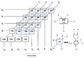
Figure 7 Layout of Carry Save Adder
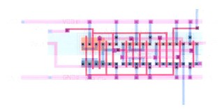
Fig 6 Architecture of 4 bit muIltiplierJSER
5.9 Verification of circuit for power savings through
simulation
Simulations of the circuit are done in Cadence SPECTRETM. The results can be compared with that of the circuit without applying the technique with same set of test vectors.All PO’s are verified so that the circuit functionality is correct. Out TTS based method was verified and found power savings for ISCAS’85 benchmark circuits according to Table 3.
5.10 Simulation Results and Discussion
We implemented the algorithm designed in the previous sections in the on ISCAS’85 Benchmark circuits. The Following Table 4 shows the number of clusters before and after the partitioning of the circuit. The estimated run time leakage savings before and after the Partitioning clearly indicates slight decrease as we need to sacrifice for cost savings. The partitioning process reduced the number of clusters from 486.8 to 18.9 on the average. This greatly saves the area of sleep transistors because we need to insert more sleep transistors if the number of clusters is more. The average number of logic gates per each cluster increased which is prior expected from 5.68 to 79.7.The average cost function reduced from 125.76% to 11.96 %. The partitioning of the circuit reduces the average run time leakage power savings from 90.57% to 84.08% .the average cost function is greatly reduced through which we can save lots of overhead area and minimum sacrifice of the delay of the circuit.
Figure 8 Layout of ripple carry adder
6.1 Architecture of the Multiplier
A 16 bit multiplier takes two 16 bit operands as input and generates 32 bit result. The implementation of multiplier is nothing but addition of partial products. Adders are used to design the multiplier. As an example 4 bit multiplier architecture is shown in Figure 6 below. Two types of adders are used as hardware elements namely Carry Save Adder(CSA) and Ripple carry adder (CPA).The carry save adder (shown as square box) adds partial products AB(AND gate shown in the Figure 6) with input carry Ci and sum Si.The output of CSA is So (sum),Co (carry). Ripple carry adder (CPA) is a normal full adder that adds A, B and Ci and gives So and Co output. A regularity is maintained such that the output So of a particular CSA is given as input Si to the CSA below it.The Co of each CSA is given as input Ci of bottom left CSA.In the last stage the So and Co of the
IJSER © 2013 http://www.ijser.org
International Journal of Scientific & Engineering Research, Volume 4, Issue 12, December-2013
ISSN 2229-5518
31
Circuit | No of Gates | Max Delay (Ps) | No of Clusters | No of Gates per Cluster | Leakage Estimated | Estimated cost |
Circuit | No of Gates | Max Delay (Ps) | Prior | Later | Prior | Later | Prior | Later | Prior | Later |
c432 | 160 | 981 | 40 | 14 | 3.8 | 10.86 | 89.4% | 88.6% | 20.2% | 10.9% |
c499 | 202 | 856 | 14 | 11 | 15.4 | 19.6 | 81.4% | 81.1% | 12.5% | 10.5% |
c880 | 360 | 821 | 212 | 15 | 1.7 | 24.0 | 88.4% | 80.7% | 86.3% | 14.1% |
c1355 | 546 | 833 | 29 | 24 | 19.6 | 23.7 | 89.8% | 89.1% | 13.4% | 11.4% |
c1908 | 880 | 1027 | 369 | 18 | 2.5 | 51.25 | 92% | 85.1% | 107.3% | 14.3% |
c2670 | 1193 | 1468 | 434 | 22 | 2.9 | 57.2 | 92.4% | 86.2% | 98.4% | 13.3% |
c3540 | 1669 | 1648 | 748 | 16 | 2.3 | 107.5 | 92.3% | 83.8% | 169.5% | 13% |
c5315 | 2307 | 1519 | 781 | 15 | 3.1 | 161.4 | 91.4% | 79.7% | 209.8% | 4.4% |
c6288 | 2416 | 4553 | 872 | 41 | 2.7 | 57.4 | 97.2% | 92.0% | 97.5% | 12.3% |
c7552 | 3512 | 1259 | 1369 | 13 | 2.8 | 294.8 | 91.4% | 74.5% | 442.7% | 15.4% |
Average | 1105.7 | 1496.5 | 486.8 | 18.9 | 5.68 | 79.7 | 90.57% | 84.08% | 125.76% | 11.96% |
Witho IWitJh
SavingSWithout
WEith
Savin
WRithou
With
Savin
overhea
Total power Runtime Leakage power Dynamic Power
Area
Circuit
ut TTS
(µW)
TTS
(µW)
(%)
TTS
(µW)
TTS
(µW)
g
(%)
t TTS
(µW)
TTS
(µW)
g
(%)
d
(%)
c432 | 75.42 | 51.52 | 31.67 | 35.83 | 6.84 | 80.9 | 39.46 | 32.98 | 16.42 | 30.2 |
c499 | 178.94 | 112.53 | 37.11 | 101.45 | 22.83 | 77.49 | 80.45 | 68.35 | 15.04 | 13.1 |
c880 | 141.53 | 115.41 | 18.45 | 66.01 | 10.9 | 83.48 | 75.43 | 2.14 | 4.36 | 21.1 |
c1355 | 210.12 | 152.14 | 27.59 | 102.12 | 16.12 | 84.21 | 109.41 | 72.43 | 33.7 | 24.23 |
c1908 | 346.34 | 243.45 | 29.7 | 142.34 | 23.36 | 83.58 | 205.12 | 163.5 | 20.31 | 17.13 |
c2670 | 496.43 | 276.43 | 44.3 | 241.53 | 30.12 | 87.5 | 256.43 | 200.2 | 21.95 | 14.21 |
c3540 | 510.12 | 275.12 | 46.06 | 310.53 | 43.30 | 86.05 | 298.34 | 232.2 | 22.19 | 10.1 |
c5315 | .106512 | 626.46 | 45.18 | 511.3 | 90.32 | 82.33 | 556.29 | 523.3 | 5.90 | 9.72 |
c6288 | 838.41 | 785.03 | 64.1 | 455.12 | 66.90 | 85.3 | 385.12 | 202.7 | 47.4 | 6.2 |
c7552 | 1600.35 | 795.23 | 50.30 | 728.59 | 74.21 | 89.8 | 879.12 | 712.2 | 18.93 | 6.17 |
Avg | 546.28 | 343.292 | 39.4 | 269.48 | 38.49 | 84.04 | 288.51 | 228.2 | 20.62 | 15.22 |

Table 4: Results of partitioning algorithm with reduced number of clusters , Estimated leakage savings and reduced cost .
last CSA are connected to four ripple carry adders to obtain the final product value. The CPA adder is a normal full adder. The output of a particular CPSA (Co ) is given as input CPA (Ci) on the right side of it.Generally a 4-bit multiplier needs a 4 X 4 CSA’s arranged as array and 4
CPA’s.The critical path extends through 4 CSA’s to
propagate So and 4 CPA’s to propagate Co .
6.2 Design of multiplier layout without TTS method.
The layouts of CSA and CPA are hand drawn in Cadence Tool. The Layouts are shown in figure Figures 7 and 8. The layouts are slightly adjusted so that the input ports and output ports are properly lined up to make connections easier as shown in Architecture diagram. The final shape of the 16 bit multiplier is made rectangular by slightly
IJSER © 2013 http://www.ijser.org
International Journal of Scientific & Engineering Research, Volume 4, Issue 12, December-2013
ISSN 2229-5518
32
modifying the layouts accordingly. Figure 9 shows complete
layout of the multiplier without TTS method. Although the final layout looks more complex it is actually easy with two building blocks CSA and CPA with appropriate connections between them.
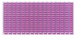
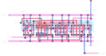
Figure 9: complete Layout of multiplier without TTS
method
are 16 arrays of CSA elements: clusters 0 to 15.Also the array
of CPA elements form the 17th cluster .The TTS of CPA cluster is Propagation delay of Co of the entire chain of CPA’s.The start time of CPA’s TTS id further shifted by delay of Co of a CSA element in the 15th cluster. Over all there are 17 clusters in the multiplier circuit. The Architecture is shown in Figure 10.
6.3 Designing multiplier layout with TTS method. According to the method proposed based on Transient Time Slot (TTS) in the previous sections of this chapter the multiplier architecture should be understood at the logic gate level. The logic gates within the total circuit of the multiplier should be partitioned into clusters after
calculating the Transient Time Slot (TTS) of them.
Figure 10 Clusters in TTS applied multiplier.
The Layout of the multiplier consists of Control transistors added to each cluster and Latches to the primary out puts. After the layout is generated Leakage savings are calculated. The TTS based Partitioning algorithm is implemented for the multiplier to form the clusters. As the multiplier is regular in shape we could easily partition the multiplier into clusters depending on its modularity. From Figure 6 we can understand that each CSA row forms a cluster whose TTS is Propagation delay of So of the CSA element. The start time of TTS for the entire CSA cluster is off by the Co delay of a CSA element in the next clock cycle.16 clusters exist as there
Figure 11 pMOS control signals for first four clusters
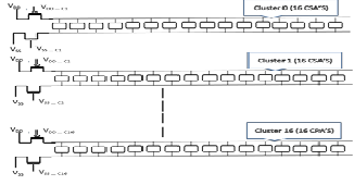
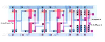
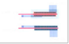
Figure 12 Layout of the control signal Shifter for remaining clusters.
Figure 13 Layout of a pair of control Transistors
IJSER © 2013 http://www.ijser.org
International Journal of Scientific & Engineering Research, Volume 4, Issue 12, December-2013
ISSN 2229-5518
33
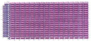
Figure 14 Layout of multiplier with TTS Method.
6.4 Calculation of TTS for each cluster
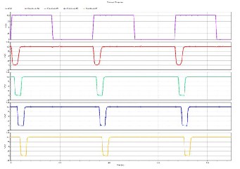
The TTS width is defined by the propagation delay of So and Co of the CSA element (horizontally).To calculate the propagation delays CSA and CPA elements are simulated in SPECTRETM environment. After the simulations we obtain the timing offsets of the control signals to be given to the clusters. As discussed earlier we doubled the TTS width. This also compensates the delay contributed by the control transistors. Figure 11 shows the global clock and control
signals for the pMOSFET for the first four clusters. The
13 shows layout of control transistors of a cluster whose sizes are 30 times that of the minimum size.
7 Results and Discussion
We designed the layout of the multiplier with and without the TTS based leakage reduction method. Cadence Layout extractor is used for the extraction of netlists. Both the circuits are simulated and verified in CADENCE SPECTRETM. To calculate the total power, runtime leakage power and dynamic power Synopsis Nanosim is used. Table
5 shows the comparision between both the circuits. The multiplier implemented with TTS method saves 54.68% of the total power consumption, 86.64% of run time leakage power and 38.54% of dynamic power. The delay increased by 6.74 % with the implementation of the technique Area increased by 8.79% because of the extra control transistors and other control logic used in the design. Among ISCAS’85 benchmark c6288 is transistor netlist of a 16 bit multiplier. The netlist is simulated and the power savings are compared with that of the layout design results. The results
are shown in Table 6.The runtime power saving is same for
IJSER
frequency of clock is 300MHZ.The TTS width is 260ps with
an offset time of 120 ps between a pair of clusters. The overlap time to switch on two nearby clusters is 140ps(260-
120).The control signals for all 16 clusters of CSA are of
same width. For the cluster 16 (CPA’s) which occurs on the second half of the clock cycle we use both and clk.
6.5 Layout Design implementing TTS method
Layouts are generated in CADENCE. The supply voltages to each CSA,CPA becomes virtual VDD and virtual VSS .The substrate of each CSA /CPA are connected to VDD and VSS (global).There are two power supplies in the layout. Figure 12 shows layout of CSA.P-SUB-CONTACT and N- SUB-CONTACTS are connected to VDD and VSS .These supplies are virtual and are connected to global power lines through control transistors for each cluster. For each Cluster a pair of control transistors and clock generator are added. For each cluster the shifting offset is same (120ps) corresponding to the previous cluster. Let us understand how control signals are generated for each cluster. A clock generator is given to cluster 0. Then a signal shifter circuit which consists of a switch and inverters are used to generate an offset of 120 ps for control signals between two clusters. The complete layout of the multiplier implementing TTS method is shown in Figure 14.The control transistors; signal shifter and generators are on the left side of the layout.Figure 12 shows the control signal shifter circuit for the remaining 15 clusters with offset value of 120ps. Figure
both layout and netlist approach which proves that out
method is acceptable when applied with ideal netlist or standard libraries. The dynamic power is more for layout based approach by 8.86% because of the parasitic capacitances. The dynamic power consumption is determined by the clock frequency which is 300 MHz for layout based design and 200 MHz for netlist approach
.Hence the layout design has 33% higher clock rate than the
netlist. For that reason the dynamic power consumption is
more for layout design. All this put together there is only
9.64% more total power savings for netlist approach. The
layout design consumes more area because of additional routing for power supplies, control transistors and control signal generators.
8 CONCLUSION
We proposed a novel runtime leakage power reduction based on Transient time slot based method which also reduced dynamic leakage and also standby leakage current. The power savings on ISCAS’85 circuits are discussed. Also layout power savings are compared with ideal transitor netlist and found that the proposed method is valid.Still issues like noise margin relating to TTS method should be investigated. Also static timing analysis can be included in the TTS method itself so that more leakage savings can be achieved.
IJSER © 2013 http://www.ijser.org
International Journal of Scientific & Engineering Research, Volume 4, Issue 12, December-2013
ISSN 2229-5518
34
| Area (µm2) | Delay (ps) | Total Power (µW) | Runtime Leakage (µW) | Dynamic Power (µW) |
Without TTS | 6381 | 2982 | 1088.69 | 336.86 | 751.92 |
With TTS | 6935.65 | 3182.98 | 492.7 | 51.74 | 461.41 |
Variation | +8.79% | +6.74% | - 54.68% | - 84.64% | - 38.54% |
Table 5 Comparison of performance parameters of multiplier with and without TTS method
| Area (µm2) | Delay (ps) | Total Power (µW) | Runtime Leakage (µW) | Dynamic Power (µW) |
Layout Design | 8.79% | 6.74% | 54.68% | 84.64% | 38.54% |
c6288 Netlist | 6.2% | 6.3% | 64.1% | 85.3% | 47.4% |
Table 6 Performance comparison of layout design versus c6288 netlist
REFERENCES
[1] A. Agarwal, S. Mukhopadhyay, A. Raychowdhury, K.
Roy, anD C. H. Kim. Leakage Power Analysis and
Reduction for Nanoscale Circuits. IEEE Micro, 6(2):68–
80, 2006.
[2] T. Raja, V. D. Agrawal, and M. L. Bushnell. Minimum
Dynamic Power CMOS Circuit Design by a Reduced
Constraint Set Linear Program. In Proc. of the 16th Int’l. Conf. on VLSI Design, pages 527–532, Jan. 2003.
[3] L. Wei, Z. Chen, M. Johnson, K. Roy, and V. De. Design and Optimization of Low Voltage High Performance
[4] Dual Threshold CMOS Circuits. In Proc. of the IEEE/ACM Design Automation Conf., pages 489–494, June 1998.K. Elissa, “Title of paper if known,” unpublished.
[5] S.Bhunia, N. Banerjee, Q. Chen, H. Mahmoodi, and K.
Roy. A Novel Synthesis Approach for Active Leakage
Power Reduction Using Dynamic Supply Gating. In Proc. Of the ACM/IEEE Design Automation Conf., pages 479–484, June 2005.
[6] D. Duarte, Y. F. Tsai, N. Vijaykrishnan, and M. J. Irwin.
Evaluating Run-time Techniques for Leakage Power
Reduction. In Proc. of the 7th Asia and South Pacific
and 15th Int. Conf. on VLSI Design, pages 31–38, 2002.
IJSER © 2013 http://www.ijser.org