International Journal of Scientific & Engineering Research, Volume 5, Issue 7, July-2014 1055
ISSN 2229-5518
Three Phase Two Switch High Power Factor
Buck Converter
Nimi N P, K Premelakumari
Abstract— This paper presents Three phase two switch buck converter with high input power factor. The key feature of the proposed converter is the switches in the converter have lower peak voltage stress compared to conventional three phase single switch buck converter.The voltage stress in the proposed converter is limited to the peak value of the phase voltage of the input capacitors rather than the peak value of the line-to-line voltage, as is the case in the conventional converter. The reduction in the voltage stresses is therefore almost half as compared to that of conventional converter. This allows lower rated, standard devices to be used in the converters and reduces switching losses. In the paper, the steady state operation of the converter is proposed and general properties and design considerations are discussed. The feasibility of the proposed converter is confirmed with simulation results.
Index Terms— AC–DC converter, low-power converter, low power three-phase converter, pulse width modulated (PW M) converter, rectifier, switch-mode power supply, three-phase converter.
—————————— ——————————
1 INTRODUCTION
ower electronic converters are widely used in applicatios such as machine drives welding ,HVDC ,battery charging etc. operating from the utility mains can generate current
harmonics that are injected into the mains may cause the mains voltage to become distorted.The dramatic growth in the use of electrical equipment in recent years has resulted in a greater need to limit these harmonics to meet regulatory standards. This can be done by some form of power factor correction (PFC) to shape the input phase currents so that they are sinusoidal and in phase with the phase voltages.
Single-phase and three-phase ac–dc power converters can be implemented with PFC for low-power and high-power appli- cations, respectively .The simplest and least expensive method of PFC is done by adding inductors and capacitors to diode- bridge rectifiers to increase the conduction angle of the input current [1]–[6], but the filter components are large and very bulky. It is also difficult to tune the filter, unless the line and ac source impedances are known. Active methods of PFC are therefore preferred over passive methods as they result in smaller, less bulky converters. Single-phase ac–dc PFC con- verters use one main power switch to perform PFC, while a six-switch converter is typically used to perform three-phase active PFC by processing the bulk of the power fed to the load or just a fraction of it as an active filter. For ac–dc power con- verters operating at a power level just high enough for three- phase converters to be considered as a better option than sin- gle-phase converters, the use of a six switch converter instead of a single-switch converter results in a significant increase in cost and complexity due to the increase in the number of ac- tive switches and the sophisticated control techniques needed.
————————————————
• Nimi N P is currently pursuing masters degree program in Power electron- ics engineering in Government Engineering College,Trissur,kerala,India
PH-+918089128604. E-mail: niminp33@gmail.com
• K Premelakumari working as Associative professor,Government Engineer-
ing college,Trissur, kerala,India, PH-+9496428795. E-mail:
kpk.kumari@gmail.com
Therefore, researches have been motivated to proposed and develop cheaper and/or simpler methods of performing three-phase active input PFC with less than six switches.
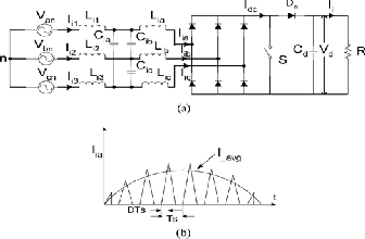
Fig. 1. (a) Conventional three-phase, single-switch ac–dc single boost converter.(b) Idealized input inductor current wave- form.
For power converters of 6 kW or less(a range just high enough where three-phase converters are a better option than single-phase converters), cheaper and simpler methods of per- forming three-phase active input PFC have been developed using converters with less than six switches [2]-[6]. One such converter, first proposed in [7], is the single switch boost con- verter shown in Fig. 1(a). The converter is operated with a constant duty cycle throughout the line cycle and is designed so that the phase currents are discontinuous and bounded by a sinusoidal envelope, as shown in Fig. 1(b). The phase currents are essentially sinusoidal currents with high frequency com- ponents that can be filtered out.
It is possible to use reduced switch buck-type converters such as the ones proposed in [8]-[11]. Especially attractive is the single-switch converter shown in Fig. 2 since it is simple and inexpensive. This converter and other buck-type convert- ers like it, however, have a drawback that has restricted their
IJSER © 2014 http://www.ijser.org
International Journal of Scientific & Engineering Research, Volume 5, Issue 7, July-2014 1056
ISSN 2229-5518
use to a limited number of applications - the switch has a very large peak voltage stress that can easily exceed 1400 -1600 V even though the output voltage can be made to be lower than the input voltage.
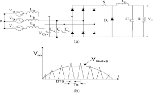
Fig. 2 (a) Conventional three-phase, single-switch ac–dc single buck converter,(b) Idealized input-capacitor voltage wave- form
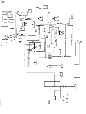
In order to overcome the limitations of the conventional single-switch buck-type converter and other topologies that are based on it, the three-phase, two-switch rectifier shown in Fig. 3 will be proposed in the paper. is explained in detail and analysed mathematically. A design procedure that can be used to select key converter component values for steady-state op- eration is developed, and then, demonstrated with an exam- ple. Finally, results obtained from an experimental prototype that was built based on the design example are proposed to confirm the feasibility of the proposed converter.
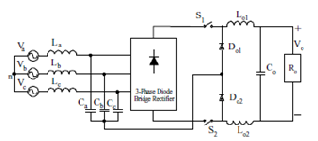
Fig. 3 Proposed three-phase two-switch rectifier
2. CONVERTER OPERATION
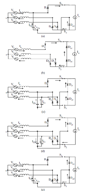
The peak voltage stress of the switches in conventional buck converters can be reduced if the switches are exposed to phase voltages instead of line voltages. This is the main oper- ating principle behind the proposed converter. The proposed converter goes through six main modes during a switching cycle. Fig. 4 shows the equivalent circuits of the various oper- ating modes.
Fig. 4. Converter operating modes (a) Mode 1: [t0-t1], (b) Mode 2: [t1-t2]and Mode 5: [t4- t5], (c) Mode 3: [t2-t3], (d) Mode 4: [t3- t4],(e) Mode 6: [t5-Ts].
Consider the case when phase input voltage Van is at its peak value and phase voltages Vbn and Vcn are both negative and equal in magnitude to one-half of Van
.
2.1 Circuit Operation for D>0.5
Mode 1(t0-t1) Fig. 4(a): At time t = t0, the switch S1 is turned on. On the ac side, the input capacitor Ca starts to dis- charge through output diode Do2. The output diode Do1 is
IJSER © 2014 http://www.ijser.org
International Journal of Scientific & Engineering Research, Volume 5, Issue 7, July-2014 1057
ISSN 2229-5518
completely off. The switch S2 is conducting from the previous mode and its current is IS2= Ib+Ic. The voltage of input capaci- tors Cb and Cc is already zero. The current through switch S1 is Is1=Io. At the end of this mode, the input capacitor Ca com- pletely discharges and VCa is zero.
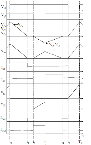
Mode 2(t1-t2) Fig. 4(b): At time t = t1, all the input capaci- tors, Ca, Cb and Cc, are completely discharged. The bridge diodes D1, D2 and D6 are conducting. Both switches S1 and S2 are conducting such that Is1=Ia and IS2= Ib+Ic. Both output diodes Do1 and Do2 are also conducting and their respective currents are IDo1= Io-Ia and IDo2=Io-(Ib+Ic).
Fig. 4 Key waveforms for the operating modes of the converter during one switching cycle for D >.5
Mode 3(t2-t3) Fig. 4(c): At time t = t2, the switch S2 is turned off, the input capacitors Cb and Cc start to charge up and the voltage across each capacitor starts to increase. The bridge diodes D2 and D6 turn off. The output current is supplied by the switch S1 and through Do1. The current through output diode Do2 is IDo2= Io
Mode 4(t3-t4) Fig. 4(d): At time t = t3, switch S2 is turned on and the current through it is Is2=Io. The bridge diodes D2 and D6 start to conduct. At the end of this mode, input capacitors Cb and Cc completely discharge and voltages VCb and VCc
are zero.
Mode 5(t4-t5) Fig. 4(b): This mode is similar to Mode 2. All
the input capacitors, Ca, Cb and Cc, are completely dis-
charged. The bridge diodes D1, D2 and D6 are conducting.
Both switches S1 and S2 and both output diodes Do1 and Do2
are conducting to provide the output current.
Mode 6(t5-Ts) Fig. 4(e): At time t = t5, switch S1 is turned
off, input capacitor Ca starts to charge up and the voltage
across capacitor Ca starts to increase. The bridge diode D1
turns off. The output current flows through output diode Do1,
switch S1 and through Do1.The current through output diode
Do2 is IDo2= Io.
2.2 Circuit Operation for D<0.5
Detailed The duty cycle of the converter decreases with the reduction in load. When it becomes less than 0.5, there are intervals when none of the switches is on, these intervals are (t2-t3) and (t5-Ts) as shown in Fig. 5
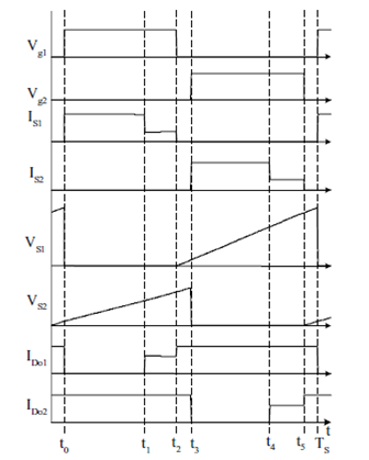
Fig. 5 Key waveforms for the operating modes of the converter during one switching cycle for D <.5
3. COMPARISON OF SWITCH VOLTAGE STRESSES
To compare the switch voltage stresses of the conventional and the proposed converter, input capacitor voltage wave- forms must be taken into account. Consider the operation dur-
IJSER © 2014 http://www.ijser.org
International Journal of Scientific & Engineering Research, Volume 5, Issue 7, July-2014 1058
ISSN 2229-5518
ing a switching cycle for the case when phase input voltage Van is at its peak value and phase voltages Vbn and Vcn are both negative and magnitude of Vbn > Vcn. Fig. 6 shows the input capacitor voltages VCa, which is positive, while VCb and VCc are negative and instantaneous value of VCb is high- er than that of VCc.
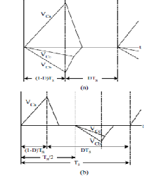
Fig.6 Voltages across input capacitors Ca, Cb and Cc (a) Single-switch buck converter (b) Proposed two-switch buck converter
The switch voltage stress in this converter is determined by the peak line-to-line voltage across input capacitors. For this case, the switch voltage stress will be difference of positive and negative voltage (largest of VCb or VCc ) and i.e. VCa- VCb. Generalizing the switch voltage stress by considering phase ‘a’, maximum voltage across input capacitor Ca is given as
 (1)
(1)
and the peak voltage of diode bridge rectifier is
 (2)
(2)
The maximum voltage across the switch is therefore given as
 (3)
(3)
the two-switch buck converter is briefly described here.
During the first half of the switching cycle, when the switch S1
is off, the input capacitor Ca charges up with the voltage pro-
portional to voltage of phase ‘a’ and when this switch is
turned on, Ca discharges till VCa reduces to zero. During the
second half of the switching cycle, the operation is repeated
for switch S2. The input capacitor voltage waveforms are
shown in Fig. 8(b). For this converter the voltage stress across
switch S1 is peak value of VCa and voltage stress across switch S2 is peak value of VCb (largest of VCb or VCc)
.Generalizing, the maximum voltage across the switch be- comes
 (4)
(4)
The proposed converter has the following features:
(i) The peak voltage stress of the switches in the pro- posed converter is almost half that of a switch in a conventional single-switch converter so that the need for higher rated, less optimal devices is avoided.
(ii) The two switches operate with 180 phase shift be- tween them, which forces the input as well as out- put inductors operate at double the switching fre- quency. This results in the reduction of the size of the inductors.
(iii) Since there are two switches, the proposed converter can operate over a wider load range with high power factor than the conventional single-switch converter. The converter can therefore operate in heavy load applications without compromising power quality.
(iv) The converter is considerably simple. The control of the converter can also be simple and a technique where the converter's duty cycle is relatively con- stant over the line cycle can be used.
The design of the converter should ensure a good power factor over the complete range of line and load conditions while trying to keep the peak voltage stress of the switches as small as possible. Therefore, in order to design the converter, the following design considerations should be taken into ac- count
4. DESIGN CONSIDERATIONS
(i) Input Capacitors: The input capacitor value directly af- fects the power factor and the operating range of the convert- er. The input capacitors Ca, Cb, Cc should be small enough so that the voltages across them are discontinuous to achieve high input power factor and minimum THD. Under light load conditions, as the duty cycle tends to get smaller, the input capacitors have less time to discharge completely and hence the operation can shift to continuous voltage mode (CVM), which is undesirable. It is therefore important to consider light load conditions when designing the input capacitors.
(ii) Switch Voltage Stress: The switch voltage stress for this converter is inversely proportional to the value of input capac- itors as stated by equations (1) and (4). Larger input capacitor values will result in the capacitors being charged to lower voltages and thus lower switch voltage stress.
(iii) Switching Frequency: Operation at higher converter switching frequencies will decrease the values of the input and output inductors and thus the size of the overall converter
IJSER © 2014 http://www.ijser.org
International Journal of Scientific & Engineering Research, Volume 5, Issue 7, July-2014 1059
ISSN 2229-5518
Higher switching frequency operation also means that the input capacitors will have less time to discharge. This will cre- ate a need for smaller input capacitor values, which can in- crease the voltage stress of the switches.
5. SIMULATION RESULT
Simulation result of proposed converter was built to confirm its feasibility. The converter was implemented with main cir- cuit components La=Lb=Lc=2.2 mH, Ca=Cb=Cc=50 nF, Lo1= Lo2=1.0 mH and Co=1000 μF, switching frequency of fs = 25 kHz. Fig. 8(a) to 8(d) waveforms obtained with the converter operating with input voltage Vin=173 VLLrms, output voltage Vo=100 V, output power Po=500W. It can be seen from Fig.
8(a) that a nearly sinusoidal input current waveform can be obtained. Fig. 8(b) shows the converter switch current and voltage waveforms.
It should be noted that the voltage across the switch is tri- angular, which is characteristic of three-phase, buck convert- ers operating in DCM as the voltage across each input ac side capacitor drops to zero due to the charging and discharging of these capacitors. It should also be noted that the switch cur- rent dips and becomes equivalent to the Phase A current a short time after the switch is turned on.
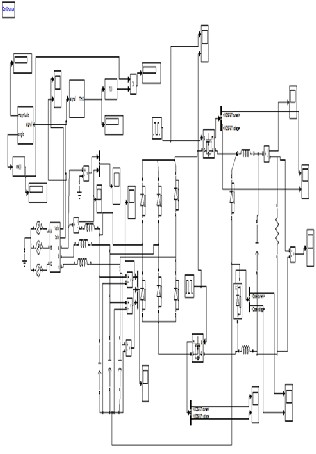
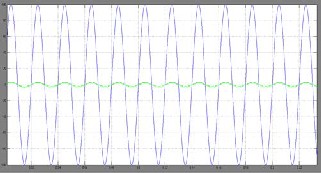 Fig. 8 Simulink model of proposed converter
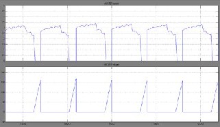
Fig. 8(a) Input phase Voltage and current 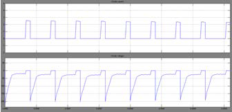
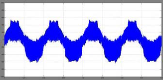
Fig. 8(c) Diode current and voltage
Fig. 8(c) Diode current and voltage
Fig. 8(b) Switch current and voltage
Fig. 8(d) Capacitor voltage
IJSER © 2014 http://www.ijser.org
International Journal of Scientific & Engineering Research, Volume 5, Issue 7, July-2014 1060
ISSN 2229-5518
sponding phase voltage of input capacitors rather than peak value of line to line voltage in conventional converter. Control of the circuit is simple and ensures good power factor and reduction in harmonics even at reduced load. New topology gives almost sinusoidal current waveform.
ACKNOWLEDGMENT
The authors wish to express their sincere thanks to Dr. M Nandhakumar, Dr. R AnasRaj, Associative Professors, De- partment of Electrical and Electronics, Government Engineer- ing College, Trissur, Kerala and Mr. Jithin K R, Excicutive En- gineer, Electrical Department, MRF Tyres, Chennai.
Fig. 9 Controlled output circuit
Fig. 9 Controlled output circuit model
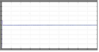
Fig. 9(a ) Controlled outputvoltage
The controlled output circuit shown in Fig. 9 and Controlled output voltage is shown in Fig. 9(a).
REFERENCES
[1] R.Prasad, P. D. Ziogas, and S. Manias, “A passive input current waveshap- ing method for three-phase diode rectifiers,” in Proc. IEEE APEC Conf.,
1991, pp. 319–330
[2] ] A. W. Kelley and W. F. Yadusky, “Rectifier for minimum line-current har- monics and maximum power factor,” IEEE Trans. Power Electron., vol. 7, no.
2, pp. 332–341, Apr. 1992
[3] B. Singh, B. N. Singh, A. Chandra, K. Al-Haddad, A. Pandey, and D. P. Ko- thari, “A review of three-phase improved power quality AC-DC converters,” IEEE Trans. Ind. Appl., vol. 51, no. 3, pp. 641–660, May/Jun. 2004.
[4] Y.Nishida and K. Mino, “A simple passive PFC scheme for three-phase diode rectifier,” in Proc. Power Convers. Conf. (PCC), 2007, pp.1294– 1301
[5] N. Takeuchi, K. Matsui, F. Ueda, and H.Mori, “A novel PFC circuit using ladder type filter employing only passive devices,” in Proc. IEEE APEC Conf.,
2008, pp. 1005–1009.
[6] O. A. Ahmed and J. A. M. Bleijs, “Three phase passive bridge rectifier with low distortion input current and boosted DC output voltage,” in Proc.UPEC Conf., 2008, pp. 1–5..
[7] A. R. Prasad, P. D. Ziogas, and S. Manias, “An active power factor correction technique for three-phase diode rectifiers”, IEEE PESC Conf., pp. 83- 92, Janu- ary 1991
[8] Y. Jang and R. W. Erickson, “New single-switch three-phase high power factor rectifiers using multi-resonant zero current switching”, IEEE Trans. on Power Elec., vol. 13, no.1, pp. 194- 201, January 1998.
[9] J. Shah and G. Moschopoulos, “A novel three-phase single-switch buck-type rectifier”, IEEE APEC Conf., vol.1, pp. 515-521, March 2005.
[10] S. Bassan and G. Moschopoulos, “A three-phase single-switch high power factor buck-type converter operating with softswitching”, IEEE PESC Conf., pp. 3053-3059, June
[11] Y. Jang, D. L. Dillman, and M. M. Jovanovic, “Three-phase isolated high power factor rectifier using soft-switched two switch forward converter”, IEEE APEC Conf., pp. 809-815, February 2007
[12] Sondeep K. Bassan, Dunisha S. Wijeratne, and Gerry Moschopoulos, “A three-phase reduced-switch high power factor buck-type converter”,IEEE Trans. on Power Elec.,vol.25,no.11,pp.November 2010.
6. CONCLUSION
The new three phase two switch buck converter overcomes the peak voltage stress of conventional converter. The peak volt- age stress is almost half of the conventional converter.Peak voltage stress of proposed converter is the peak value of corre-
IJSER © 2014 http://www.ijser.org