International Journal of Scientific & Engineering ResearchVolume 2, Issue 10, October-2011 1
ISSN 2229-5518
Eduardo B. Tibayan Jr.,Gil Nonato C. Santos
Abstract—CdS nanomaterials were successfully synthesized at varying furnace angle of 0°, 45°, and 90° with a growth temperature of 8000C and dwell time of 8 hours using the vapor phase crystal growth technique. The synthesized product was a yellow-orange material and was characterized using the SEM, EDX, and photoluminescence spectroscopy. The SEM photomicrographs revealed various nanostructures in a form of nanowires. Energy dispersive X-ray analyses confirmed that CdS nanomaterials showed a uniform composition of Cd and S with a minimal presence of impurities. The PL spectra of the samples revealed intense peaks in the range of 477 nm to 548 nm wavelengths where the energy band gap was obtained at
2.44 eV which is approximately that of CdS.
Keyword —CdS nanomaterials, furnace angle, vapor phase crystal growth technique
————————————————————
anotechnology is a field of applied science and technology whose theme is to control materials and
to fabricate devices on the atomic and molecular scale, generally between 1 and 100 nanometers[1]. This is a highly multidisciplinary field, benefiting from the efforts and developments in many fields like medicine and sciences. In the near future, nanoelectronic devices may replace microelectronics in communication and comput- er industries with nanostructures [2]. The emerging field of nanotechnology, materials and devices on the nanos- cale, has the potential to take different fields further than ever imagined [3]. This is possible because reducing the size of a material to nanoscale proportions alters its bulk electronics, magnetic, and optical properties [4], [5].
In the past decade, the synthesis and characterization
of controlled shape and structure nanometersized metal sulfide has been attracting an increasing interest because of their excellent physical and chemical properties, which are not available in their bulk material. Among these ma- terials, CdSnanocrystalline, as semiconductors, are im- portant because of their potential applications in photo- electronic transition devices[6], [7], [8].
Cadmium Sulfide (CdS), an important II-VI semicon- ductor, shows important applications in different fields
————————————————
Eduardo B. Tibayan Jr., currently pursuing PhD in Physics, De La Salle
University-Manila, Philippines. E-mail:sir_ed26@yahoo.com
Gil Nonato C. Santos, Doctor of Philosophy in Materials Science, Profes-
sor, De La Salle University-Manila, Philippines. E-mail:
especially in optical devices. The enhanced properties of CdS enable multiple new applications including the inte- gration of nanomaterials into nanodevices such as bio- logical labeling[9], photovoltaic (PV) solar cells[10], las- ers[11], light emitting diodes (LED)[12], optoelectronic devices, and a wide array of photosensors[13].
At present, there are numerous reports on the prepa-
ration of CdS nanoparticles like nanowires[14], [15], [16],nanorods[17], [18], quantum dots[14], [19], thin films [20], [21], [22], nanobelts[23], [24], dendrites [25], nano- ribbons [28], nanospheres,nanoshuttles, nanotubes[29] and other nanostructures. Several deposition methods and techniques were employed including the ultrasonical colloidchemistry deposition [20], metalorganic chemical vapor deposition [21], hydrothermal treatment [25], [26], [27], thermal evaporation [28], Solvothermal method[15], [16], chemical bath deposition[22], gas diffusion[30], mi- croemulsions[18], reverse micellesystems[29], sol-gel route[31],in situ simultaneous copolymerization- sulfidation[32], liquid-phase deposition[33] and irradia- tion[34]. Some of the methods used are very time con- suming and others result in a textured film. In this work we demonstrate the use of vapor phase crystal growth technique as a simple and affordable way of preparation of CdS nanomaterials.
IJSER © 2011 http://www.ijser.org
International Journal of Scientific & Engineering ResearchVolume 2, Issue 10, October-2011 2
ISSN 2229-5518
The procedure started with the sealing of one end of the quartz tube using a high temperature blowtorch (mixture of LPG and oxygen). After which, it was cleaned using an ultrasonic cleanserfor 30 minutes,
rinsed, and dried. Approximately 0.035 grams of high
purity CdS powder (99.99%) was loaded into the quartz tube and was connected to the Thermionics High Va- cuum System for sealing at a high vacuum pressure of
≈10-6Torr as seen in Fig.1.
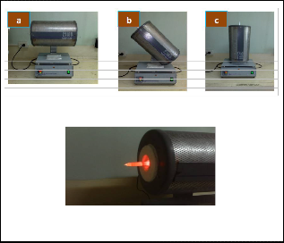
Fig. 2Furnace set at different angle a) 00, b) 450, and c) 900
Fig. 3 Set-up for growing the CdS nanomaterials at furnace set at 00
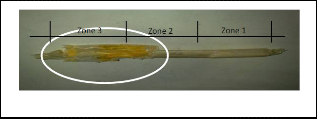
Once the quartz tube has already cooled down to room temperature, it was slowly cracked in a fumehood environment. Fragments of the cracked quartz tube with deposits of CdS nanomaterials (Fig. 4) were subjected for
characterization.
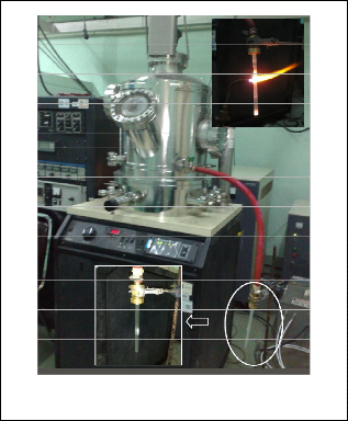
Fig. 4 Deposit CdS nanomaterials in a cracked quarts tube
Fig. 1 Quartz tube connected to the high vacuum system. Inset shows the sealing of the quartz tube.
The sealed quartz tube was placed in a tube fur- nace and was baked at a constant ramp rate of 80 mi- nutes. The furnace was programmed at growth tem- perature of 800 0C, dwell time of 8 hours, ramp rate and was set at varying angles (0, 45, 90) as shown in Fig. 2. To maintain a gradient necessary for the growth of nanomaterials, the quartz tube was inserted half- way through the furnace with zone 1 completely in- side as presented in Fig. 3. Zone 2 is at the opening and zone 3 is outside the furnace. This caused the CdS powder at the hotter end (zone 1) to evaporate and condense at the colder part (zone 2 and 3) of the quartz tube. The quartz tubes were then allowed to
cool down to room temperature.
The deposited CdS nanomaterials were characterized using the SEM, EDX and PL equipment as seen in Fig.
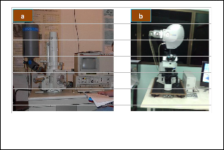
5.The effect of the varying furnace angle will be analyzed by comparing the SEM images, EDX analyses and PL spectra of the grown nanomaterials.
Fig.5. Instruments used in CdS nanomaterials cha- racterization, a) Scanning Electron Microscope, and b) Spectral Microscope
IJSER © 2011 http://www.ijser.org
International Journal of Scientific & Engineering ResearchVolume 2, Issue 10, October-2011 3
ISSN 2229-5518
Fig.6revealed the SEM images of various nanostruc- tures prepared at different furnace angle (00, 450, and
900),with constant growth temperature of 8000C and
dwell time of 8 hours. Cotton like nanowires are ob- served at a furnace angle of 00 with a diameter ranging from 181 nm to 403 nm. Fewer nanowires but smaller in diameter with dimensions of around 30-68 nm were syn- thesized at a furnace angle of 450. A prominent image of the nanowires is formed when the furnace angle is in the vertical position with diameter range of 14-50 nm.
An increase in furnace angle leads to a greater
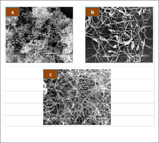
amount of dissociated CdS circulating within the tube
involving the upward and downward movement in re- sponse to gravity, resulting to subsequent condensation and formation of nanostructures. This explains why emi- nent nanostructures such as nanowires are observed at higher furnace angle.
The deposition of CdS nanomaterials in lower tem- perature zone can be attributed to the angle between gravitational field and orientation of tube as affected by temperature gradient. The value of acceleration due gravity inside the quartz tube with respect to tempera- ture gradient is proportional to furnace angle as shown in Fig. 7.
Fig. 6 SEM images of various nanostructures prepared at 800 0 C temperatures with dwell time of 8 hours and different furnace angle a) 00,b) 450, and c) 900.
IJSER © 2011 http://www.ijser.org
International Journal of Scientific & Engineering ResearchVolume 2, Issue 10, October-2011 4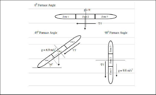
ISSN 2229-5518
Fig. 7 Diagram of the angle between gravitational field with respect to temperature gradient and orientation of tube
Fig. 8 shows the stoichiometric amount of CdS sample
(69.46% Cd and30.54% S) at a growth temperature of 800
0C, dwell time of 8 hours and furnace angle of 00. At the
450 furnace angle, a 61.79% Cd-38.21% S was obtained while 71.45% Cd-28.55% S atomic percentage was ob- served in the samples grown at 900. Based on the results, atomic and elemental composition of CdS nanomaterials
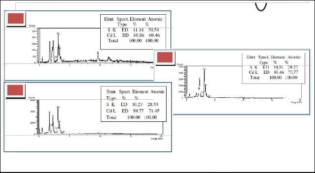
were affected by furnace orientation.
a
b
c
Fig.8Energy Spectrum of the sample synthesized at different furnace angle a) 00,b) 450, and c) 900
IJSER © 2011 http://www.ijser.org
International Journal of Scientific & Engineering ResearchVolume 2, Issue 10, October-2011 5
ISSN 2229-5518
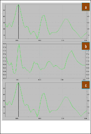
Fig. 9 shows the PL spectra of the samples prepared with growth temperature of 800 0C, dwell timeof 8 hours and with varying furnace angle. The wavelength peaks recorded are 513.40 nm, 507.64 nm, and 507.57 nm for the furnace angle of 00, 450, and 90 0respectively. The average energy band gap of CdS nanostructures was calculated to be 2.44 eV. This is also very close to the theoretical value of CdS energy band gap.
Fig. 9 Photoluminescence Spectra of the Nanomaterials different furnace angle, a) 00, b) 450, and c) 90 0
Cadmium Sulfide nanomaterials were successfully synthesized at varying furnace Angle using the Vapor Phase Crsytal Growth Technique. The study was able to characterize the surface morphologies and elemental and atomic composition of the nanomaterials using SEM and EDX, respectively. Photoluminescence spectra were also determined using spectral microscope.
From the results of the SEM, various nanostructures
were formed when the growth conditions were va- ried.The deposition of CdS nanomaterials in lower tem- perature zone can be ascribed to the orientation of tube
as affected by thermal gradient and gravitational field.
Increasing the growth conditions increases the variety and amount of nanomaterials and produces lengthy but smaller in diameter nanomaterials specifically the nano- wires. EDX analyses also showed that cadmium percen- tage increased when the diameter of nanowires is small- er. Optical properties of CdS nanomaterials were obtained by the photoluminescence spectra. Minimal deviations were observed in different furnace angles. The difference can be attributed to artifacts in the sample.
This work became possible through the supportof the
Commision on Higher Education, Philippines.
[1] Polizzi, and M. Meneghetti, “Free silver nanoparticles synthe- sized by laser ablation in organic solvents and their easy func- tionalization,” Langmuir, vol. 23, pp. 6766–6770, 2007.
[2] Y. Xia, P. Yang, Y. Sun, Y. Wu, B. Mayers, B. Gates, Y. Yin, F.
Kim and H. Yan, ”One-Dimensional Nanostructures: Synthe- sis, Characterization andApplications”,Adv.Mater.vol.15, pp.
353-389,2003.
[3] J.H. Zhan, X.G. Yang, S.D. Li, D.W. Wang, Y. Xie and Y.T. Qian, “Achemical solution transport mechanism for one-dimensional growth of CdSnanowires”, Journal of Crystal Growth, vol.220, pp. 231-234, 2000.
[4] J. Milam, L. Lauhon and J. Allen, “Photoconductivity of Semi- conducting CdSNanowires”, Nanoscape, vol.2, pp. 43-47, 2005.
[5] H.S. Yang, S. Santra, and P.H. Holloway, “Synthesis and appli- cation ofMndoped II–VIsemiconductor nanocrystals”, J. Nanos- ci. Nanotech,vol. 5,pp.364–1375, 2005.
[6] V.L. Colvin, M.C. Schlamp, and A.P. Alivisatos, Nature,
vol. 370pp. 354, 1994.
[7] D.L. Klein, R. Roth, A.K.L. Lim, A.P. Alivisatos, and
P.L.McEuen, Nature,vol. 389, pp. 699, 1997.
[8] B.A. Ridley, B. Nivi, and J.M. Jacobson, Science, vol.286, pp.
746, 1999.
[9] W.J. Parak, D. Gerion, T. Pellegrino, D. Zanchet, C. Micheel, S.C. Williams, R. Boudreau, M.A. Le Gros, C.A. Larabell, and A.P.Alivisatos, Nanotechnology, vol. 14, R15, 2003.
[10] I. Visoly-Fisher, S.R. Cohen, D. Cahen, and C.S. Ferekides,
“Electronically active layers and interfaces in polycrystalline devices: crosssection mapping of CdS/CdTe solar cells”, Appl. Phys. Lett.vol. 83,pp. 4924, 2003.
[11] V.I. Klimov, A.A. Mikhailovsky, S. Xu, A. Malko, J.A. Hol- lingsworth, C.A. Leatherdale, H.-J. Eisler, and M.G. Bawendi, Sciencevol. 290, pp. 314, 2000.
[12] C.W. Lee, C.H. Choub, J.H. Huang, C.S. Hsu, and T.P.
Nguyen,” Investigations of organic light emitting diodeswith
CdSe(ZnS) quantum dots”,Materials Science and Engineeringvol.
147, pp. 307–311, 2008.
[13] H.S. Nalwa, Encyclopedia of Nanoscience and Nanotechnolo- gy, American Scientific Publishers, New York, 2003.
[14] J. Dilag, H.Kobus, and A. Ellis, “Cadmium sulfide quantum dot/chitosan nanocomposites for latent fingermarkdetec- tion”,Forensic Science International,vol. 187, pp. 97–102, 2009
IJSER © 2011 http://www.ijser.org
International Journal of Scientific & Engineering ResearchVolume 2, Issue 10, October-2011 6
ISSN 2229-5518
[15]J. Yao, G. Zhao, D. Wang, and G. Han, “Solvothermal synthesis and characterization of CdS nanowires/PVAcomposite films”, Materials Letters, vol. 59, pp. 3652 – 3655,2005.
[16] G. Xu, H. Wang, C. Cheng, H. Zhang, J. Cao, and G. Ji, “Synthe-
sis of single crystalline CdS nanowires with polyethylene gly- col 400 as inducing template “, Transaction of Nonferrous Metals Society of Chinavol. 16, pp. 105-109, 2006.
[17] H. Zhang, D. Yang, X. Ma,Y.Ji, S. Li, and D.Que,“Self-assembly of CdS: from nanoparticles to nanorodsand arrayed nanorod bundles”, Materials Chemistry and Physics,vol. 93, pp. 65–69,
2005.
[18]Q. Zhang, F. Huang, and Y. Li, “Cadmium sulfide nanorods formed in microemulsions”, Colloids and Surfaces A: Physico- chem. Eng. Aspects vol. 257–258, pp. 497–501, 2005
[19]J. Mao, J. Yao, L. Wang, and W. Liu, “Easily prepared high-
quantum-yield CdS quantum dots in water usinghyperbran- chedpolyethylenimine as modifier”, Journal of Colloid and Inter- face Science,vol. 319, pp. 353–356, 2008.
[20] H. Cui,M. Costa,V. Teixeira, and J. Zhang, “Solution-Grown Method of CdS Film by Ultrasonical Colloid Chemistry Depo- sition Technique”, International Journal of Photoenergyvol. 2006, Article ID 24916, pp. 1–4, 2006
[21]H.Uda, H.Yonezawa, Y.Ohtsubo, M.Kosaka and H.Sonomura, “Thin CdS films prepared by metalorganic chemical vapor de- position”, Solar Energy Materials and Solar Cells,vol. 75, issues 1-
2, pp. 219-226, 2003.
[22] M. Karimi, M.Rabiee, F.Moztarzadeh,M.Tahriri, and M.Bodaghi, “Controlled synthesis, characterization and optical properties of CdSnanocrystalline thin films via chemical bath deposition (CBD) route”, Current Applied Physics, vol. 9 pp.
1263–1268, 2009.
[23]T. Gao, and T.H. Wang, Journal of Physics and ChemistryB,vol.
108, pp. 20045–20049, 2004
[24] J. Zhang, F.H. Jiang, and L. Zhang Journal of Physics and Chemi- stryB, vol. 108, pp. 7002–7005, 2004.
[25] Q. Wang, G. Xu, and G. Han, “Synthesis and Characterization of Large-Scale Hierarchical Dendrites of Single-Crystal CdS”, Crystal Growth & Design, vol. 6 ,pp 1776–1780, 2006.
[26]F. Chen, R. Zhou, L. Yang, N. Liu, M. Wang, and H. Chen,
“Large-Scale and Shape-Controlled Syntheses of Three- Dimensional CdS”, Journal of Physics and Chemistry C, vol. 112 (4), pp 1001–1007, 2008.
[27] M.Salavati-Niasari, M. Reza Loghman-Estarki, and F.Davar, “Controllable synthesis of nanocrystallineCdS with different morphologies byhydrothermal process in the presence of thioglycolic acid”, Chemical Engineering Journal, vol. 145,pp.
346–350, 2008.
[28] S.Kar, B. Satpati, P. V. Satyam, and S. Chaudhuri, “Synthesis and Optical Properties of CdSNanoribbons”, Journal of Physics and ChemistryB, vol. 109 (41), pp 19134–19138, 2005.
[29]X. Yang, Q. Wu , L.Lia, Y. Ding, and G. Zhang, “Controlled synthesis of the semiconductor CdS quasi- nanospheres,nanoshuttles, nanowires and nanotubes by the reverse micellesystems with different surfactants”, Colloids and
Surfaces A: Physicochem. Eng. Aspects,vol. 264, pp. 172–178, 2005
[30]B.Zhanga, Y.Shena, A. Xiea,L.Yanga, and X. Wanga, “Shape controlled synthesis of CdS nanostructures in tungstosilicatea- cid solution by a novel approach”, Materials Chemistry and
Physics, vol. 116, pp. 392–399, 2009
[31]B.T. Holland, C.F. Blanford, T. Do, and A. Stein, Chem. Matervol.
11, pp. 795, 1999
[32]S.H. Liu, X.F. Qian, J. Yin, H.A. Xi, Z.H. Huang, and Z.K. Zhu, “Fabrication of CdS nanocrystals embedded in copolymer ma- trix byan in situ simultaneous copolymerization-sulfidation technique”, Materials Science and Engineering B, vol. 98, pp.
99/103, 2003.
[33]M.Hsua, I.Leub, Y.Suna, and M. Hon, “Fabrication of CdS-TiO2 coaxial composite nanocablesarrays by liquid-phase deposi- tion”, Journal of Crystal Growth, vol. 285, pp. 642–648, 2005
[34] J.Hea,X.Zhaoa, J.Zhua,and J. Wang, “Preparation of CdS nano-
wires by the decomposition of thecomplex in the presence of microwave irradiation”, Journal of Crystal Growth, vol. 240, pp.
389–394, 2002.
[35] G. Cao, Nanostructures & Nanomaterials: Synthesis, Properties & Applications, London: Imperial College Press, 2004
IJSER © 2011 http://www.ijser.org