𝑃𝑙𝑖𝑖 = 2
(𝑔𝑚 + 𝐺𝑑𝑠 𝐴𝑣 )2𝑉𝑠 2𝑅𝐿
International Journal of Scientific & Engineering Research, Volume 5, Issue 2, February-2014 78
ISSN 2229-5518
The Effect of Temperature on the Nonlinearity of pHEMTs
Brendan C. Ubochi, Ali A. Rezazadeh
Abstract— An understanding of the nonlinearity caused by a change in temperature is important in the design of microwave circuits, most of which are designed using pseudomorphic high electron mobility transistors (pHEMTs). The approach used here is to extract the Taylor series coefficients of the nonlinear drain current and then calculate the values of these coefficients at different temperatures. The calculated coefficient values are then used to obtain and analyse the output powers.
Index Terms— Intermodulation distortion, temperature characterization, semiconductor device modelling.
—————————— ——————————
GaAs-based pHEMTs are gaining wide applications for high- efficiency power amplification as well as applications requiring low noise figures and high gain, particularly at
Also, the expression for the fundamental output power and IMD products of a pHEMT amplifier which is based on (2) is given by[7]:
millimeter-wave frequencies[5]. As such, an understanding of
the nonlinearity caused by a change in temperature is
(3)![]()
𝑃𝑙𝑖𝑖 = 2
(𝑔𝑚 + 𝐺𝑑𝑠 𝐴𝑣 )2𝑉𝑠 2𝑅𝐿
important in the design of microwave circuits.
𝑃𝐼𝑀𝐷2 =
(𝑔𝐼 + 𝐺 𝐼 𝐴2 +2𝑚
𝐴 )2𝑉 4 𝑅
In this study, the pHEMT presented is a (0.5×200µm2) AlGaAs/InGaAs/GaAs double channel pHEMT. An analysis
(4)![]()
8 𝑚
𝑑𝑠 𝑣
11 𝑣
𝑠 𝐿
1 𝐼𝐼 + 𝐺 𝐼𝐼 𝐴3 + 3𝑚
𝐴2 + 3𝑚
𝐴 ))2𝑉 6 𝑅
(5)
of the pHEMT output power is presented and data regarding
the temperature effects on the Taylor series coefficients is
provided.
𝑃𝐼𝑀𝐷3 = 128 (𝑔𝑚
𝑑𝑠 𝑣
12 𝑣
21 𝑣
𝑠 𝐿
We use the Curtice quadratic drain current model[2] to model
the drain current, 𝐼𝑑𝑠 of the pHEMT, given as:
𝐼𝑑𝑠𝐹𝐸𝑇 = β( Vgs – VTO)2 tanh(αVds)(1 + λVds) for Vgs ≤ Vpf![]()
ψ + 1
We use the d.c measurement data obtained from the Research
Group at the School of Electrical and Electronic Engineering,![]()
� ε ��V
– V �
University of Manchester. The modelled drain current values are
𝐼𝑑𝑠 = 𝐼𝑑𝑠𝐹𝐸𝑇 �1 −
ψ + 1
gs pf
2 � for Vgs > Vpf
calculated from (1). The optimum parameter values are obtained
(1)
β�Vgs – VTO �
by minimizing the sum of the squared errors between the
measured values and the calculated/modelled values. However, the beta and alpha for the output characteristic is 0.058 and 0.008
where Vpf denotes the point on the transfer characteristic
where the transconductance begins to degrade, α represents
the fitting parameter between the linear and the saturated region, β is the transconductance parameter, λ is the output conductance parameter and it models the slope of the curve in the saturation region, ψ is the exponent of the empirical
transconductance degradation parameter, ε is the empirical transconductance degradation parameter, VTO is the pinch-off voltage [4][9]. Other parameters have their usual meanings. The small signal incremental drain current can be represented by[9]:
respectively. The optimized parameter values for the model are in
Table 1.
Fig. 1 shows good agreement between the measured and modelled drain currents. The analysis that follows depends on the
𝐼𝑑𝑠 data at 𝑉𝑔𝑠 values from -1V to +0.6V. This is to prevent the error at 𝑉𝑔𝑠 = -1.2V in Fig. 1a from propagating to other values
during differentiation. The trans-conductance is obtained by
differentiating the drain current with respect to the gate to source
voltage at constant 𝑉𝑑𝑠 , in this case, 𝑉𝑑𝑠 = 3V and in saturation.
The output conductance is obtained by differentiating the drain
current with respect to the drain voltage. The cross-terms are
1 𝐼
2 + 𝐺 𝐼 𝑣 2 + 2𝑚
𝑣 𝑣 )
![]()
𝑖𝑑𝑠 = 𝑔𝑚 𝑣𝑔𝑠 + 𝐺𝑑𝑠 𝑣𝑑𝑠 +
(𝑔𝑚 𝑣𝑔𝑠
𝑑𝑠
𝑑𝑠
11 𝑔𝑠
𝑑𝑠
calculated by first differentiating with respect to 𝑉𝑑𝑠
and at
1 𝐼𝐼 3
𝐼𝐼 3
2 + 3𝑚
𝑣2 𝑣
) (2)
constant 𝑉𝑑𝑠 , differentiated with respect to 𝑉𝑔𝑠 [7].![]()
+ 6(𝑔𝑚 𝑣𝑔𝑠 + 𝐺𝑑𝑠 𝑣𝑑𝑠 + 3𝑚12𝑣𝑔𝑠 𝑣𝑑𝑠
21 𝑔𝑠
𝑑𝑠
Table 1
𝐼 𝐼𝐼
The fitting parameter values for the nonlinear drain current.
where the 𝑔𝑚 terms 𝑔𝑚 , 𝑔𝑚 , and 𝑔𝑚
are respectively, the
transconductance, the second and third order derivatives with
𝐼 𝐼𝐼
respect to 𝑉𝑔𝑠 . The 𝐺𝑑𝑠 terms 𝐺𝑑𝑠 , 𝐺𝑑𝑠 R and 𝐺𝑑𝑠 R are respectively, the
output conductance, the second and third order derivatives with
respect to 𝑉𝑑𝑠 . The coefficients 𝑚11 = ∂𝑔𝑚 /∂𝑣𝑑𝑠 = ∂𝐺𝑑𝑠 /∂𝑣𝑔𝑠 , 𝑚12 =
2 𝐼
𝐼 2
∂2𝑔𝑚 /∂𝑣𝑑𝑠 = ∂𝐺𝑑𝑠 /∂𝑣𝑔𝑠 and 𝑚21 = ∂𝑔𝑚 /∂𝑣𝑑𝑠 = ∂2𝐺𝑑𝑠 /∂𝑣𝑔𝑠 are the
cross-terms.
IJSER © 2014 http://www.ijser.org
International Journal of Scientific & Engineering Research, Volume 5, Issue 2, February-2014 79
ISSN 2229-5518
to determine the values of the Taylor series coefficients at different temperatures. It is important to note that the cross terms
were also found to vary with temperature in the same way as 𝐺𝑑𝑠 . The temperature coefficients for 𝑚11, 𝑚12 and 𝑚21 are -0.359 × 10-
,-0.36 × 10
and -0.37× 10 , respectively. The cross terms are
3 -3 -3
80
70
60
50
40
30
20
10
0
-10
Vds =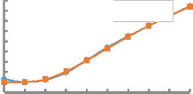
-1.2 -1 -0.8 -0.6 -0.4 -0.2 0 0.2 0.4 0.6
obtained by first differentiating the drain current with respect to the drain voltage before differentiating with respect to the gate voltage. This accounts for the similarity of their temperature
coefficients with 𝐺𝑑𝑠.
Equations for the linear output power and intermodulation products (IMD) in (4) – (6) are used to calculate the output powers.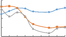
0
-20
-40
(a) The transfer characteristic of the 0.5 × 200µm2 GaAs DCh pHEMT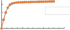
30
-60
-80
-1 -0.8 -0.6 -0.4 -0.2 0 0.2 0.4 0.6
20 Vgs = -0.2V
10
0
0 2 4 6
(b) The output characteristic of the 0.5 × 200µm2 GaAs DCh pHEMT![]()
![]()
Fig. 1. The transfer characteristic (a) and the output characteristic (b) of the 0.5 × 200µm2 GaAs DCh pHEMT, showing a close match between the measured and simulated results. Simulated , Measured
In the temperature range, -25oC to 125oC, all equivalent circuit parameters and indeed the physical parameters show a linear temperature dependent relationship expressed as [1][8]:
P(T) = P(To )[1 + β(T – To )]………………………….......(6)
where β is the temperature coefficient in units per degree, To is the reference temperature in oC, and P(To ) is the value of the parameter at the reference temperature. The temperature
coefficients of 𝑔𝑚 and 𝑅𝑑𝑠 are -1.44 × 10⁻³ and 0.39 × 10⁻³
respectively[8]. From 𝑅𝑑𝑠 , the temperature coefficient of 𝐺𝑑𝑠 is
calculated as -0.36 × 10⁻³. These temperature coefficients are used
Figure 2 shows the linear output power, the second and third order IMD products. It appears Fig. 2 does not accurately model the IMD2 and IMD3. However, it is important to note that intermodulation products are both bias and load dependent[3][6].
It is suggested[3] that an increase in 𝑉𝑑𝑠 leads to a decrease in the IMD products due to 𝐺𝑑𝑠 . It is also observed that the cancellation points (dips) in the IMDs are delayed or postponed as 𝑉𝑑𝑠 is
increased![]()
![]()
Fig. 2. Fundamental( ),second order( ) and third order
( ![]() ) IMD output levels of a (0.5×200µm2)
) IMD output levels of a (0.5×200µm2)
AlGaAs/InGaAs/GaAs double channel pHEMT biased at 𝑉𝑑𝑠 =
3V.
There is also some nulling when 𝑉𝑑𝑠 is increased. These, in addition to measurement errors, may account for the
reduction in IMD2 and IMD3 powers at 𝑉𝑑𝑠 = 3V, and also the
delay in the cancellation effects of the second and third order
𝐺𝑑𝑠 and 𝑔𝑚 terms.
IJSER © 2014 http://www.ijser.org
International Journal of Scientific & Engineering Research, Volume 5, Issue 2, February-2014 80
ISSN 2229-5518
100
50
0
-50
-100
-150
-200
-40 -20 0 20 40
series coefficients of the nonlinear drain current in analysing the effect of temperature on the nonlinearity of pHEMTs has been demonstrated. The factors and interactions that lead to a reduction in the pHEMTs’ output power have also been analysed. The analysis presented in this paper is important as the data provided can be used in the design optimization of pHEMT devices for future high performance power amplifiers.
The first author would thanks Prof. M.O. Kolawole for finding the time to review this work and for his comments andencouragement.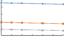
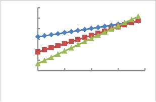
(a) Output power at 25oC and 𝑃𝑖𝑖 = -40dBm to 35 dBm
10
0
-10
-20
-30
-40
-25 0 25 50 75 100 125
![]()
![]()
(b) Temperature = -25oC to 125oC, 𝑃𝑖𝑖 = 5dBm,𝑉𝑔𝑠 = -0.2 V Fig. 3. Fundamental( ),second order( ) and third
![]()
order ( ) IMD output levels of a (0.5×200µm2)
AlGaAs/InGaAs/GaAs double channel pHEMT biased at 𝑉𝑑𝑠
= 3V.
A regression analysis shows that the fundamental output power depends mostly on the trans-conductance and voltage
gain (𝐴𝑣 ), both are highly negatively correlated. The variation
.
[1] Anholt, R., Electrical and Thermal Characterization of MESFETs, HEMTs and HBTs. Norwod:Artech House, 1995.
[2] Curtice, W.R., “A MESFET Model for Use in the Design of GaAs
Integrated Circuits,” IEEE Microwave Theory and Techniques,Vol.
28.pp. 418 – 45,1980.
[3] Higgins, J.A., Kuvas, L.R.,”Analysis and improvement of Intermodulation Distortion in GaAs Power FETs,” IEEE Transactions on Microwave Theory and Techniques,Vol. MTT-28, 1980.
[4] Glover, I., Microwave Devices, Circuits and Subsystems for
Communications Engineering. England: John Wiley & Sons, 2005.
[5] Kolawole M.O. and Ogunti E.O., Electronics:An Engineering
Course.Ibadan: Spectrum[in press], 2013.
[6] Parker, A.E and Qu, G.,” Intermodullation Nulling in HEMT Common Source Amplifiers,” IEEE Wireless and Microwave Componenets Letters. Vol. 11, No. 3., 2001.
[7] Qu, G. ,”Characterizing Intermodulation in High Electron Mobility
Transistors,” Doctoral Thesis, 1998.
[8] Tan J.P. et al.,”Temperature Dependent Small signal Model Parameters Analysis of AlGaAs/InGaAs pHEMTs in Multilayer 3D MMIC Technology,” In Proceedings of the 5th European Microwave Integrated Circuits Conference, pp 174 – 177 ,2010.
𝐼 𝐼
of IMD2, it was found, depends almost equally on 𝑔𝑚 and 𝐺𝑑𝑠
[9] Ubochi B.C., “The Effect of Temperature on the Nonlinearity of
𝐼𝐼
𝐼𝐼
while the IMD3 depends slightly more on 𝐺𝑑𝑠 than 𝑔𝑚 . It is
known that the contribution of the 𝐺𝑑𝑠 terms dominate at low
input powers while the 𝑔𝑚 terms dominate at high input
powers [3]. The statistical results give some insight as to the
extent to which these terms affect the variation of the total
output powers.
With the exception of the IMD2, the output powers showed
very little difference when the cross terms were removed. Fig.
3 shows calculated output powers at 𝑃𝑖𝑖 = 5dBm for different
temperatures using Taylor series coefficient values at those
temperatures. It is easy to see in the Figure that the linear
output power and the intermodulation products decline
steadily as temperature increases. The converse is also true.
This is due mainly to the negative temperature coefficients of
the terms that contribute to these output powers.
The use of temperature coefficients of the extracted Taylor
pseudomorphic High Electron Mobility Transistors,” M.Sc.
Dissertatation, University of Manchester, 2011.
IJSER © 2014 http://www.ijser.org