International Journal of Scientific & Engineering Research Volume 4, Issue 1, January-2013 1
ISSN 2229-5518
Speed Power and Area Efficent VLSI
Architectures of Multiplier and Accumulator
Naveen Kumar, Manu Bansal, AmandeepKaur
Abstract—This paper describes the comparison of VLSI architectures on the basis of Speed, Area and Power of different type of Adders like Carry Chain Adder, Carry Look Ahead Adder, Carry Skip Adder, and Carry Select Adder and 32-bit pipelined Booth Wallace MAC Unit with Carry Chain Adder, Carry Look Ahead Adder, Carry Skip Adder, and Carry Select Adder is designed in which the multiplication is done using the Modified Booth Wallace algorithm and the pipelining is done in the Booth Multiplier and Wallace Tree to increase the speed. All Adder and MAC are described in VHDL and synthesized the circuit using 90 nm standard cell library on FPGA and Synopsys Design Compiler. As an hardware implementation all the adder and MAC are implemented on FPGA with test benches to cover all cases on Spartan 3E kit with LCD and Keyboard interfacing.
Index Terms—Multiplier, Adder, Pipelining, High-speed, modified Booth algorithm, Synopsys Design Compiler, FPGA.
————————————————————
he core of every microprocessor, DSP, and data- processing ASIC is its data path. Statistics showed that more than 70% of the instructions perform additions and multiplications in the data path of RISC machines [1]. At the heart of data-path and addressing units in turn are arithmetic units, such as adders, and multipliers. Multiplication based operations such as Multiply and Accumulate and inner prod- uct are among some of the frequently used Computation- Intensive Arithmetic Functions, currently implemented in many DSP applications such as convolution, fast Fourier trans- form, filtering and in microprocessors in its arithmetic and logic unit. Since multiplication dominates the execution time of most DSP algorithms, so there is a need of high speed mul- tiplier. The demand for high speed processing has been in- creasing as a result of expanding computer and signal pro-
cessing applications.
Pipelined MAC based on Booth Wallace with Carry Select
Adder is one of the fastest MAC Unit and Pipelined MAC
with Carry Look Ahead Adder and MAC with Carry Skip
Adder require the low power and less area. Modified Booth
algorithm reduces the number of partial products to be gener-
ated and is known as the fastest multiplication algorithm and
many researches on the multiplier architectures including ar-
ray, parallel and pipelined multipliers have been pursued
which shows that pipelining is the most widely used tech-
nique to reduce the propagation delays of digital circuits. Finally, the basic operation found in MAC is the binary addi- tion. Therefore, binary addition is the most important arithme- tic operation. It is also a very critical one if implemented in
hardware because it involves an expensive carry-propagation step, the evaluation time of which is dependent on the oper- ands.
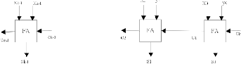
This is the simplest design in which the carry-out of one bit is simply connected as the carry-in to the next [1]. It can be im- plemented as a combination circuit using n full-adder in series as shown in Fig 1 and is called ripple-carry adder.
The latency of k-bit ripple-carry adder can be derived by con- sidering the worst-case signal propagation path. As shown in Fig 2 the critical path usually begins at the x0 or y0 input pro- ceeds through the carry-propagation chain to the leftmost FA and terminates at the sk-1 output.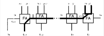
The critical path might begin at c0 and/or terminate at ck. However given that the delay from carry-in to carry-out is more important than from x to cout or from cin to s, full-adder designs often minimize the delay from cin to cout, making the path as shown in Fig 2 with the largest delay. Thus the expres- sion for latency of k-bit ripple-carry adder is
Tripple-add = TFA (x, y → cout ) + (k − 2) ∗ TFA (cin → cout )
+ TFA (cin → s)
Where TFA (inputoutput) represents the latency of a full-
adder on path between its specified input and output. As an approximation to the foregoing, it can be concluded that the
latency of a ripple-carry adder is kTFA[11]. It is seen that the
latency grows linearly with k, making the ripple-carry design
undesirable for large k or for high-performance arithmetic
unit. However a carry completion detection adder takes ad-
IJSER © 2013 http://www.ijser.org
International Journal of Scientific & Engineering Research Volume 4, Issue 1, January-2013 2
ISSN 2229-5518
vantage of the log 2 k average length of the longest carry chain
to add two k-bit binary number in O (log k) time on the aver-
age.
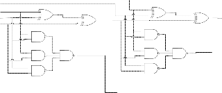
The carry-look ahead adder (CLA) [18] computes group gen- erate signals as well as group propagate signals to avoid wait- ing for a ripple to determine if the first group generates a carry or not. From the point of view of carry propagation and the design of a carry network the actual operand digits are not important. What matters is whether in a given position a carry isgenerated, propagated or annihilated. In the case of binary addition the generate (gi), propagate(pi) and annihilate(ai) signals [11][19][20] are characterized by the following logic equations:
gi = xi . yi
pi = xi yi ai = not(xi + y )
ti = xi + yi
Thus assuming that the above signals are produced and made
available, the rest of the carry network design can be based on
them and become completely independent of the operands or
even the number representation radix. Using the preceding
signals, the carry recurrence can be written as follow
ci+l = g i + ci. pi
The carry recurrence essentially states that a carry will enter
stage i+1 if it is generated in stage i. The later version of carry
recurrence leads to slightly faster adders because in binary
addition, ti is easier to produce than pi. (OR instead of XOR).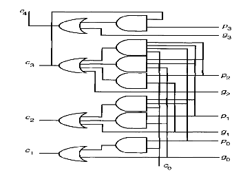
ci+l = g i + ci. t i .
practical limitations on fan-in and fan-out, irregular structure, and long wires delay [1]. The total delay of the car- ry-look ahead adder is O (log k) which can be significantly less than the carry chain adder. There is a penalty paid for this gain in term increased area. The carry- look ahead adders re- quire O (k * log k) area. It seems that a carry-look ahead adder larger than 256 bits is not cost effective. Even by employing block carry-look ahead approach, a carry-look ahead adder with 1024 bits seems not feasible or cost effective [1].
The carry skip adder (CSKA) [11][21] was invented for deci- mal arithmetic operations. The CSKA is an improvement over the ripple-carry adder. By grouping the ripple cells to- gether into blocks, it makes the carry signal available to the blocks further down the carry chain, earlier. The primary car- ry ci coming into a block can go out of it unchanged if and only if, xi and yi are exclusive-or of each other. This means that corresponding bits of both operands within a block should be dissimilar.
If xi = yi = 1, then the block generates a carry without waiting for the incoming carry signal. And the generated carry will be used by blocks beyond this block in the carry chain.
If xi = yi = 0, then the block does not generate a carry and will absorb any carry coming into it by AND all pi of a block.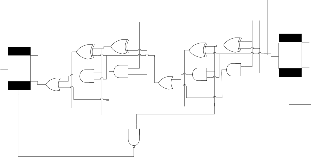
The skip signal will be generated to select between the incom- ing carry and the generated carry using a 2:1 multiplexer as shown in Fig 4. The last FA stage of a block will generate a carry, if any, before arrival of the input carry ci. When the in- put carry arrives, it needs to pass through two logic gates only so that the output carry ci+1 will stabilize.
x i+1 y i+1
x i y i
c i-1
c
s i+1
p i+1
c i
s i p i
Skip signal
Carry-look ahead adder hardware may be designed as shown in Fig 3. The carry-look ahead logic consists of two logic levels, AND gates followed by an OR gate, for each ci when the adder inputs are loaded in parallel, all gi and pi will be generated at the same time. The carry-look ahead logic allows carry for each bit to be computed independently. Ide- ally, the carry signal ci will be produced through two-stage logic at the same time, which means that the adder will have a constant time complexity. However, it is impractical to build a two stage full large-size carry-look ahead adder because of the
Subsequent blocks can have larger size so that the carry will skip more bits and the adder speed will be increased. In this case, the adder is called one-level carry-skip adder with varia- ble block sizes. The skip logic determines whether a carry entering one block may skip the next group of blocks. However, the main design problem with the adder is working out how best to group the skips.
The carry-skip adder has a simple and regular struc- ture that requires an area in the order of O (k) which is hardly larger than the area required by the ripple-carry adder. The time complexity of the carry-skip adder is bounded between O (k) and O (log k). An equal block size one-level carry-skip adder will have a time complexity of O (k). Block width tre- mendously affects the latency of adder. More number of
IJSER © 2013 http://www.ijser.org
International Journal of Scientific & Engineering Research Volume 4, Issue 1, January-2013 3
ISSN 2229-5518
blocks means block width is less, hence more delay.
The carry-select adder (CSLA) comes in the category of condi- tional sum adder. Conditional sum adder works on some con- dition this scheme; blocks of bits are added in two ways: as- suming an incoming carry of 0 or 1, with the correct outputs selected later as the block's true carry-in becomes known. With each level of selection, the number of known output bits dou- bles, and leading to a logarithmic number of levels and thus logarithmic time addition.
A single-level carry-select adder [11] is one that combines three kl/2-bit adders of any design into a k-bit adder as shown in Fig 5. One k1/2-bit adder is used to compute the lower half of the k-bit sum directly. Two k1/2-bit adders are used to compute the upper k1/2-bits of the sum and the carry-out un- der two different scenarios: Ck/2 = 0 and Ck/2 = 1. The cor- rect values for the adder's carry-out signal and the sum bits in positions kl/2 through k - 1 are selected when the value of Ck/2 becomes known. This technique of dividing adder in two stages increases the area utilization but addition operation fastens.
Where the multiplier A and multiplicand B are assumed to have n bits each and the addend Z has (2n+1) bits. A basic MAC unit as shown in Fig 6 can be divided into two main blocks [2].
Multiplier
Accumulator
Multiplication is a mathematical operation that at its simplest is an abbreviated process of adding an integer to itself a speci- fied number of times. A number (multiplicand) is added to itself a number of times as specified by another number (mul- tiplier) to form a result. A Fast Multiplication process consists of three steps [3]:
Partial Product Generation. Partial Product Reduction.
Final stage Carry Propagate Adder.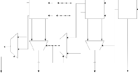
1
4-bit
1
4-bit
4-bit 0
M U X
Cout
Adder 0
M MUX U X
Z[63:60]
Adder 0
MUX
Z[7:4]
Adder
Z[3:0]
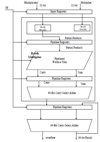
In order to improve the speed of the MAC unit, there are two major bottlenecks that need to be considered. The first one is the fast multiplication network and the second one is the ac- cumulator. Both of these stages require addition of large oper- ands that involve long paths for carry propagation.
The pipeline technique is widely used to improve the perfor- mance of digital circuits. As the number of pipeline stages is increased, the path delays of each stage are decreased and the overall performance of the circuit is improved [6]. The various pipeline schemes have been investigated to find the optimum number of pipeline stages and the positions for the pipeline registers to be inserted in modified Booth multiplier in order to obtain the high-speed.![]()
The MAC unit basically do the multiplication of two numbers multiplier and multiplicand and add that product in result stored in the accumulator. The general construction of the MAC operation can be represented by this equation:
IJSER © 2013 http://www.ijser.org
International Journal of Scientific & Engineering Research Volume 4, Issue 1, January-2013 4
ISSN 2229-5518
cand. The booth algorithm shifts and/or complements the multiplicand (X operand) based on the bit patterns of the mul- tiplier (Y operand). Essentially, three multiplier bits [Y (i+1) ,Y (i) and Y (i-1) ] are encoded into eight bits that are used to select multiples of the multiplicand [-2X,-X,0,+X,+2X] The three multiplier bits consist of a new bit pair [Y (i+1) and Y (i)] and the leftmost bit from the previously encoded bit pair [Y (i-
1)]. Grouping the three bits of multiplier with overlapping has
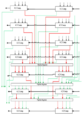
four bits. Thus a carry out is necessary and subsequently carry in. The 4:2 compressor structure actually compress five input bit into three output. The output of 4:2 compressor consists of one bit (sum) in position j and two bits in final carry and in- termediate carry in position (j+1). However a carry out is in- dependent on carry in as shown in Fig 7.
Carry in
In1
A
half partial products which improve the system speed. Radix-4 Modified Booth's algorithm [6] is:
Y (i-1) = 0; Insert 0 on the right side of LSB of multi- plier.
Start grouping each three bits with overlapping from
Y (i-1).
If the number of multiplier bits is odd, add a extra 1
bit on left side of MSB and generate partial product
In2 A
B In3
In4
cin
Ca rry
B
Sum
cin
Sum
3 XOR Gates
Carry
from Table 1.
When new partial product is generated, each partial
product is added two bit left shifting in regular se-
quence.
It is then sign extended.
TABLE 1
RADIX-4 MODIFIED BOOTH ALGORITHM [6].
Yi+1 | Yi | Yi-1 | Recoded Digit | Operand Multiplication |
0 | 0 | 0 | 0 | 0 x multiplicand |
0 | 0 | 1 | +1 | +1 x multiplicand |
0 | 1 | 0 | +1 | +1 x multiplicand |
0 | 1 | 1 | +2 | +2 x multiplicand |
1 | 0 | 0 | -2 | -2 x multiplicand |
1 | 0 | 1 | -1 | -1 x multiplicand |
1 | 1 | 0 | -1 | -1 x multiplicand |
1 | 1 | 1 | 0 | 0 x multiplicand |
Carry-Out
IJSER © 2013 http://www.ijser.org
International Journal of Scientific & Engineering Research Volume 4, Issue 1, January-2013 5
ISSN 2229-5518
Each box contains the bits that are fed into a 4:2 compressor cell. It is, however, still the most critical part of the multiplier because it is responsible for the largest amount of computa- tion. Naturally the pipeline registers should be inserted within the Wallace tree to improve the performance as shown in Fig
8.The number of partial products of the N-bit modified Booth multiplier is N/2[4][5][6]. In case of the 32-bit modified Booth multiplier, the number of partial products is sixteen. In this three stage of pipelining is used, in 1st stage sum and carry of first four rows of compressors are stored in two pipeline regis- ters. In 2nd stage these sum and carry are fed into the fifth and sixth row of compressors and their output is stored in pipeline registers. In 3rd stage the sum and carry of fifth and sixth row are added in seventh row of compressors. The Wallace tree adds four rows and generates two rows using 4:2 compres- sors. One row represents the carries and the other row repre- sents the sums.
Accumulator basically consists of register and adder. Register hold the output of previous clock from adder. Holding out- puts in accumulation register can reduce additional add in- struction. An accumulator should be fast in response so it can be implemented with one of fastest adder like Carry-look Ahead Adder or Carry Skip Adder or Carry Select Adder.
.
The 32-bit Pipelined Booth Wallace MAC has been imple- mented on Spartan XC3S500-4FG320 device and simulated using Modelsimand synthesized using 90 nm technology us- ing Synopsys Design Compiler and its results compared with the conventional MAC unit.
z : Output Data 64-bit
TABLE 2
SIMULATION RESULT VERIFICATION OF PIPELINED BOOTH WALLACE
MAC UNIT.
clk1 | clk2 | clk3 | clk4 | clk5 | clk6 | clk7 | clk8 | clk9 | |
A | 5 | 5 | 4 | 4 | 4 | 4 | 4 | 4 | 5 |
b | 3 | 3 | 3 | 3 | 3 | 3 | 3 | 3 | 7 |
Z | 15 | 30 | 45 | 60 | 75 | 90 | 105 | 117 | 129 |
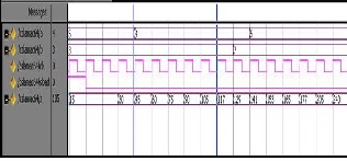
There is latency of 5 clock cycle means we get the final output of MAC in 6th clock cycle which is clear from the Table 2 and from Fig 9.
TABLE3
FPGA SYNTHESIS RESULTS OF DIFFERENT ADDERS.
However CSLA has more LUTs than CCA and CLA but less than CSKA but it has very less combinational path delay. So CSLA is the best adder architecture where the operands size is large.
TABLE 4
DC SYNTHESIS RESULTS OF CARRY CHAIN ADDER.
Adder Type | CCA | CLA | CSLA | CSKA |
Level of Logic | 66 | 64 | 23 | 67 |
Critical Path length | 9.11 | 12.13 | 4.49 | 8.68 |
Leaf Cell Count | 223 | 191 | 544 | 256 |
Total no. of NET | 352 | 319 | 673 | 385 |
Comb.Area | 1479 | 1432 | 3587 | 2057 |
Dyn. Power(uW) | 220 | 195 | 497 | 248 |
Lkg.Power(nW) | 952 | 904 | 2.14uW | 1.13uW |
CSLA has comparatively low value of critical path length hence less combinational path delay but it has higher no. of leaf cell count and combinational path area. It also has high dynamic power than other adder architectures. It’s clear from the tables that CLA and CSKA architectures can be used for
IJSER © 2013 http://www.ijser.org
International Journal of Scientific & Engineering Research Volume 4, Issue 1, January-2013 6
ISSN 2229-5518
low power applications as it has low value of dynamic as well cell leakage power.
TABLE 5
FPGA SYNTHESIS RESULTS OF 32-BIT MAC UNIT.
TABLE 7
FPGA SYNTHESIS RESULTS OF CONVENTIONAL AND PIPELINED
BOOTH WALLACE MAC UNIT
MAC | Conventional MAC | Proposed MAC |
Size | 32 bits | 32 bits |
Slice Flip- Flops | 237 | 1399 |
LUTs | 3646 | 3298 |
Delay(ns) | 24.1 | 10.5 |
Frequency (MHz) | 41.5 | 71 |
Power (mW) | 279.2 | 531.42 |
The Table 5 shows that the LUTs used in 32-bit MAC with CSLA is lesser than other MAC architectures and has higher frequency of operations. So 32-bit MAC with CSLA is best in term of LUTs and frequency of operations but it requires more power supply than other MAC architectures. However MAC with CLA require less power supply than MAC with other adder architectures.
The Pipelined MAC is synthesized using FPGA and Design Compiler. Table 7 shows the compared result of MAC synthe- sized on FPGA and Table 8 shows the results of Pipelined Booth Wallace MAC.
TABLE 8
DESIGN COMPILER SYNTHESIS RESULTS OF PIPELINED 32-BIT MAC UNIT.
TABLE 6
DC SYNTHESIS RESULTS OF 32-BIT MAC UNIT.
According to DC synthesis Results Table 6 for a fixed clock period, MAC with CLA has less value of critical path length so have less value of critical path slack as well as total negative slack value so it can run on higher frequency than other 32-bit MAC architectures. However CSKA has less value of leaf cell count and design area than other three architectures. So area and power wise the 32-bit MAC with CSKA is better as com pared to other architectures.
TABLE 9
COMPARISON W ITH OTHER 16-BIT PIPELINED MULTIPLIER REFER- ENCES [6]
`
IJSER © 2013 http://www.ijser.org
International Journal of Scientific & Engineering Research Volume 4, Issue 1, January-2013 7
ISSN 2229-5518
The design compiler results shows that in case of best case analysis (FF corner) the MAC met all the constraints at the clock period 1.1 ns or at the frequency 909.09 MHz and in worst case scenario (SS corner) all the constraints at the clock period 2.43 ns or at the frequency 411.52 MHz and in average case scenario (TT corner) all the constraints at the clock period
1.45 ns or at the frequency 689.65 MHz
This Proposed MAC is also verified with FPGA using SPAR- TAN 3E Kit. To provide 64 bit input data Keyboard interfacing is done and to see the results LCD interfacing is done with spar- tan3E kit.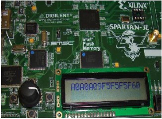
Fig10.2: LCD Display of 32-bit Booth Wallace MAC Unit.
The pipelining is the most widely used technique to improve the performance of digital circuits but power increased. We proposed architectures of the high-speed low power and less area of modified Booth Wallace MAC. CSLA has comparative- ly low value of critical path length hence less combinational path delay but it has higher no. of leaf cell count and combina- tional path area. It also has high dynamic power than CLA and CSKA. So CLA and CSKA architectures can be used for low power applications as it has low value of dynamic as well cell leakage power.
————————————————
NaveenKumar has been completed M.Tech from Thapar University Patiala in VLSI Design and CAD. E-mail: naveen209e@gmail.com
Manu Bansal is currently pursuing PHD in VLSI inThapar University,
Patiala,. E-mail: mbansal@thapar.edu
Amandeep Kaur has been completed M.Tech from Thapar University Patia-
la in VLSI Design and CAD. E-mail : amani.gem@gmail.com
[1] Koc, C.K., “RSA Hardware Implementation”, RSA Laboratories, RSA Data Security, Inc. 1996.
[2] Abdelgawad, A., Bayoumi, M., “High Speed and Area-Efficient Mul- tiply Accumulate (MAC) Unit for Digital Signal Processing Applica- tions”, IEEE International Symposium on Circuits and Systems, pp .
3199 – 3202, 2007.
[3] Fayed, Ayman A., Bayoumi, Magdy A., “A Merged Multiplier- Accumulator for high speed signal processing applications”, IEEE In- ternational Conference on Acoustics, Speech, and Signal Processing (ICASSP), pp 3212 -3215, 2002.
[4] A.D.Booth, “A Signed Binary Multiplication Technique”, Quarterly
J.MechanAppl.Math., vol.IV, 1951.
[5] Macsorley, O.L., “High-Speed Arithmetic in Binary Computers”, Proceedings of the IRE, vol. 49, pp 67 – 91, 1961.
[6] Kim Soojin; Cho Kyeongsoon; “Design of High-speed Modified Booth Multipliers Operating at GHz Ranges”, World Academy of Science, Engineering and Technology, Issue 61, January 2010.
[7] Oklobdzija, V.G.; Villeger, D.; Liu, S.S.; “A method for speed opti- mized partial product reduction and generation of fast parallel mul- tipliers using an algorithmic approach” IEEE Transactions on Com- puters, vol.45, pp 294 – 306, 1996.
[8] P. Devi and A. Girdher, “Improved Carry Select Adder with Re- duced Area and Low Power Consumption”, International Journal of Computer Applications (0975– 8887) vol. 3 – No.4, June 2010.
[9] R.P.P., Singh; B. Singh and P. Kumar, “Performance Analysis Of Fast Adders Using VHDL”, International Conference on Advances in Re- cent Technologies in Communication and Computing, 2009.
[10] A. A. A., Gutub and H. A., Tahhan, “Efficent Adders to Speedup
Modular Multiplication for Cryptography”, Computer Engineering
Department, KFUPM, Dhahran, SAUDI ARABIA, 2001.
[11] B. Parhami, “Computer Arithmetic, Algorithm and Hardware De- sign”, Oxford University Press, New York, pp.73-137, 2000.
[12] K.C. Chang, “Digital system design with VHDL and Synthesis” An integrated Approach IEE Computer Society, pp 408-437, 1999.
[13] Design Compiler User Guide v1999.10.
[14] HimanshuBhatnagar; “Advanced ASIC Chip Synthesis” using Syn- opsys Design Compiler, Physical Compiler and Prime Time, 2nd ed..Kluwer Academic Publishers, 2002.
[15] WengFook Lee, “VHDL Coding and Logic Synthesis with Synopsys” Academic Press pp.147-227, 2000.
[16] HimaBinduKommuru Hamid Mahmoodi, “ASIC Design Flow Tuto- rial Using Synopsys Tools”, Nano-Electronics & Computing Research Lab School of Engineering San Francisco State University San Fran- cisco, CA Spring 2009.
[17] Deschamps, J.P.; Bioul, G.J.A; Sutter,G.D.; “Synthesis of Arithmetic Circuits”; FPGA, ASIC and Embedded Systems, John Wily & Sons Inc., Publication, 2006.
[18] A. Weinberger; J.L. Smith, “A Logic for High-Speed Addition”, Na- tional Bureau of Standards, Circulation 591, pp. 3-12, 1958.
[19] Neil. H. E. Weste , “Principle of CMOS VLSI Design”, Adison-Wesley
1998.
[20] Raahemifar, K. and Ahmadi, M., “Fast carry look ahead adder” IEEE Canadian Conference on Electrical and Computer Engineering, 1999.
[21] Kantabutra, V., “Designing Optimum One-Level Carry-Skip Ad-
ders”, IEEE Transactions on Computers, pp.759-764, June 1993.
IJSER © 2013 http://www.ijser.org