International Journal of Scientific & Engineering Research, Volume 4, Issue 12, December-2013 260
ISSN 2229-5518
Sliding Mode Control of Wide input Wide output DC-DC Boost Converter
Narendra Bavisetti, G.Naresh, V.Satyanarayana
Abstract: Coupled inductor based DC-DC converters are used into achieve high step up(or)step down voltage gains. Most of these converters use fixed frequency pulse width modulation technique for controlling the output voltage. Many configurations are available for step up and step down DC-DC conversion operation, out of the available converter configurations the model proposed in [1] is considered for analysis purpose for which a control circuit based on sliding mode controller is proposed for implementation. This sliding mode controllers are non-linear controllers and found to be suitable for switching operations and references are provides sufficient literature about the stable operation of converter circuits. The performance of this converter is studied for different loads with indirect sliding mode controller. And case studies verified with the help of MATLAB SIMULINK software.
Keywords: Wide input wide output (WIWO), Sliding Mode Control (SMC), Indirect Sliding Mode Control, Coupled Inductor, DC-DC Converter, PWM Controller.
1. INTRODUCTION
ratio[7]-[15].
For many applications such as high intensity discharge lamp ballasts for automobile
headlamps, fuel-cell energy conversion systems,
solar-cell energy conversion systems, and battery
backup systems for uninterruptible power supplies requires DC–DC converter with a high step-up voltage gain. Theoretically, a high step- up voltage gain with an extremely high duty ratio can be achieved by dc–dc boost converter [1]–[3]. However, in practice power switches, rectifier diodes, and the equivalent series resistance (ESR) of inductors and capacitors limit step-up voltage gain to limited values. A serious reverse-recovery problem is due to the extremely high duty-ratio in dc-dc boost converter. To overcome this recovery problem so many topologies have been introduced and to provide a high step-up voltage gain without extremely high duty-ratio [4]-[24].
A simple structure with a high step-up voltage gain and an electrical isolation is dc-dc fly back converter but active switch in this converter suffers with high voltage stress due to the leakage inductance of the transformer. To minimize the voltage stress and to recycle the energy of the leakage inductance, few energy regeneration techniques are introduced[4]-[6].In these techniques, coupled-inductor technique can provide high voltage gain with a low voltage stress on the active switch of converters, and high efficiency without the problem of high duty ratio
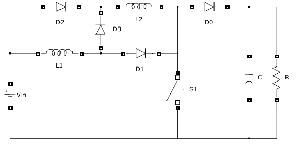
In the past research on the transformer less dc-dc converters are happened, these include cascade boost type[16],the quadratic boost type[17],the voltage-lift type[18]–[20], the capacitor-diode voltage multiplier type[21],[22],and the boost type integrating with switched-capacitor technique [23]. These techniques are all complex and are having high cost. The modified boost type with switched inductor technique is shown in Fig.1 [24].It has very simple structure because only one power stage is used in this converter. However, this converter has two issues (1) During the switch-on period, three power devices exist in the current- flow path and during the switch-off period, two power devices exist in the current-flow path and (2) The output voltage is equal to the voltage stress on the active switch.
Figure 1: Transformer less dc–dc high step-up
IJSER © 2013 http://www.ijser.org
International Journal of Scientific & Engineering Research, Volume 4, Issue 12, December-2013 261
ISSN 2229-5518
converter
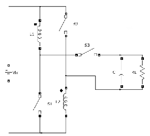
A transformer less dc–dc high step-up
converter is proposed in this paper, as shown in Fig.2, compared with the converter in [24], the proposed converter has the following merits:
1) During the switch-on period two power devices exist in the current flow path and during the switch-off period, one power device exist in the current flow path. 2)The voltage stresses on the active switches are less than the output voltage; and 3)Under the same operating conditions, including input voltage, output voltage, and output power, the current stress on the active switch during the switch-on period is equal to the half of the current stress on the active switch of the converter in[24].
These proposed dc–dc converters utilizes
switched- inductor technique, in which during the switch-on period two inductors with same level of
inductance are charged in parallel and during the
Fig.2 shows the circuit configuration of the proposed converter, consisting of two active switches (S1 and S2 ) two inductors (L1 and L2 ) with
the same level of inductance, one output diode Do
IJSER
switch-off period these are discharged in series, to achieve high step-up voltage gain without the extremely high duty ratio. The operating principles and steady-state analysis are discussed in the following sections. Some conditions are assumed to analyze the steady- state characteristics of the proposed converters and these are as follows:
1) All components are ideal and the ON-state resistance R DS(ON) of the active switches, the forward voltage drop of the diodes, and the ESRs of the inductors and capacitors all are ignored. 2) All capacitors are sufficiently large and voltages
across the capacitors can be treated as constant.
and one output capacitor Co. Switches S1 and S2
are controlled simultaneously with one control
signal. The operating principle and steady- state analysis of CCM are presented in detail as follows
Entire operation of the circuit proposed in
Fig.2 is divided into two modes.
Mode 1: Switches S1 and S2 are ON and Diode D0
is OFF and value of switching function u is 1. During this mode the two windings of coupled inductor are connected in parallel. In this mode of operation coupled inductor stores energy. Load Voltage and Current through inductor are given by
And![]()
![]()
dV0 = − V0 u dt RC
……..(1)![]()
diL =
dt
![]()
2Vin u
(1 + k ) L
……..(2)
Mode 2: Switches S1 and S2 are OFF and Diode D0
is ON and value of switching function u is 0. The two windings of the coupled inductor are connected in series and energy stored in coupled inductor is delivered to the load.
Expressions for voltage across load and
Current through the inductor are given by
IJSER © 2013 http://www.ijser.org
International Journal of Scientific & Engineering Research, Volume 4, Issue 12, December-2013 262
ISSN 2229-5518
![]()
![]()
dV0 = − V0
![]()
![]()
+ iL − iL u
And
dt RC C C
………(3)
scheme.
In direct SMC scheme output signal of the![]()
![]()
diL = − 1 V
dt 2L (1 + k ) 0
![]()
+ Vin
2L (1 + k )
![]()
+ V0 +
2L (1 + k )
![]()
3Vin u
2L (1 + k )
hysteresis circuit directly controls the switching of the power switch. Block diagram representation of indirect SMC is shown in fig.1. In indirect SMC
………(4)
Combining equations (1), (3) and (2),(4) will
give state model of proposed configuration
scheme, the output of the SM controller is first compared with an external triangular waveform.
Then the output signal of the comparator is![]()
![]()
dV0 = − V0
![]()
![]()
![]()
+ iL − iL u − V0 u
employed to switch the converter switch. In this
dt RC C C RC
And
……… (5)
case, the control signal is not applied directly to the power switch. Indirect SMC is realized by changing the modulation method of the SM![]()
diL = −
dt
![]()
1 V
2L (1 + k ) 0
![]()
+ Vin +
2L (1 + k )
---------(6)
controller from hysteresis modulation to PWM, this scheme is also known as duty cycle control. Main advantage of PWM is that by fixing the
V0
+ 3Vin
+ 2Vin u
frequency of the ramp, the frequency of the output![]()
![]()
2L(1 + k ) 2L(1 + k )
![]()
L(1 + k )
switching signal will be constant, regardless of
how the duty cycle varies with the variation of the control signal [20]. The SM controller design
process aims at determining the switch position u,
IJSEwhich generalRly has the form:
u = 1
u = 1
for s(x) > 0
for s(x) < 0
The state model of proposed configuration is
Where s(x) is a smooth scalar function or instantaneous state trajectory given by
dV0
−1 1
0
![]()
![]()
dt =
RC C V
+ V
diL
0
−1 i
![]()
1 in
2L(1 + k )
s = α1x1 + α2x2 + α3x3 = J T x
…… (1)![]()
![]()
dt 2L(1 + k )
−1
−1 0
For existence of SM operation, the reachability![]()
![]()
+ u
RC C V + V u
condition is
0
0
7 in
2L(1 + k )
![]()
2L(1 + k ) .
Lim s(x ). s(x ) < 0
s → 0
…… (2)
Two types of sliding mode control (SMC)
To achieve such control in an indirect SMC a relation between direct SMC and duty cycle is required. The system trajectory of SMC is described by means of equivalent dynamics [25].
.
techniques are available for DC-DC converters.
x = Ax + Bu + D
…… (3)
One is called the direct SMC scheme, other is known as indirect SMC scheme.
Where u is equivalent control function [26], is
.
the solution for u in the equation s(x) = 0 .
Control law that adopts a switching function is given by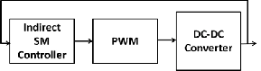
IJSER © 2013 http://www.ijser.org
![]()
u = 1 (1 + sgn (s ))
2
…… (4)
International Journal of Scientific & Engineering Research, Volume 4, Issue 12, December-2013 263
ISSN 2229-5518
Parameters of the circuit are L = 0.0011H , with coefficient of coupling = 0.95, C = 68µF , operating frequency is equal to 20kHz. β is
The objective of sliding mode control is
to regulate the output voltage Vb to a
gain constant whose value is equal to
1
![]()
2333.72
reference voltage Vref. The design of sliding mode controller for boost converter starts with the choice of sliding surface. As it is shown in [13], it is clear that direct surface V0 -Vref can be tend to zero only if the current increases continuously . The output voltage generates the reference current from voltage error and
The converter is achieving a voltage gain
approximately equal to 18.667.
Value K is determined based on trial and
error method. Relation between K and P is established with the help of polynomial approximation. Its value is given by
2.081 × 10 −9 P 3 − 4.94 × 10 −6 P 2 + 6.603 × 10 −3 P + 0.1725
![]()
K =
controls inductor current via sliding mode.
This control of the output voltage of DC-
DC converter meets the criteria of stability and
existence of sliding mode. However, it is
1.767 × 10
K p
![]()
Ratio =
β
− 7 P 2
+ 8.548 × 10
−3 P
+ 0.08521 × Ratio
difficult to determine the gains of the voltage loop since sliding mode is a highly non linear method. In order to improve the performances of the controller, we proposed to study a control mode based on a sliding surface which
involves output voltage.
P is the power delivered to the load.
Proposed circuit is simulated for different
values of load power it has been observed that the system is exhibiting good regulation characteristics for the load power variations from 100W to 750W
load regulation characteristic is shown in Table 1,
IJSER
The existence condition of sliding mode
.
along with the nominal output voltages and load
currents.
implies that both Sand
s tend to zero when t
tend to infinity, which means that the dynamics of the system will stay into the sliding surface. The existence condition of the
.
sliding mode is
s s < 0
(when S→0) the
fulfillment of this inequality ensures the existence of sliding mode around the commutation surface.
After making the simplifications and applying the above mentioned conditions parameters of magnitude of the control voltage of PWM controller is found as![]()
1 (βV0 − K p )+ V0 +
1
![]()
i L K > 1
RC βC
Where K is a constant derived based on tail error method to eliminate steady state error. Where K is constant and is a function of load power.
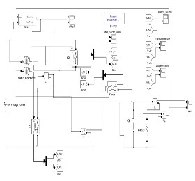
With the available stability condition DC- DC boost converter circuit with nominal output voltage equal to 220V supplying a load of 200W from 12V input supply is modeled and simulated with the help of MATLAB SIMULINK.
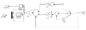
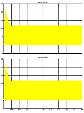
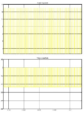
Simulation diagram is shown in Fig.4, Subsystem modeling is shown in Fig.5,Load Voltage and load current, Voltage across switches S1 , S2 and Current through diode , Voltage across D for load power P = 200Watts is shown in Fig.6, Fig.7 and Fig.8 respectively.
IJSER © 2013 http://www.ijser.org
International Journal of Scientific & Engineering Research, Volume 4, Issue 12, December-2013 264
ISSN 2229-5518
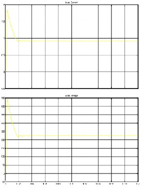
IJSEFigure 6: LoRad Current and Load voltage for P=
Figure 7: Voltages across Switches S1 and S2
IJSER © 2013 http://www.ijser.org
International Journal of Scientific & Engineering Research, Volume 4, Issue 12, December-2013 265
ISSN 2229-5518
[2]. X.Wu,J.Zhang,X.Ye,andZ.Qian,“Analysis and derivations for a family ZVS converter based
on an active clamp ZVS cell,” IEEE Trans
.Ind. Electron.,vol.55,no.2,pp.773–
781,Feb.2008.
[3]. D.C.Lu,K.W.Cheng, and Y.S.Lee,“ A single
switch continuous-conduction-mode boost
converter with reduced reverse-recovery and switchinglosses,”IEEETrans.Ind.Electron.,vol.5
0,no.4,pp.767–776, Aug.2003.
[4]. N.P.Papani kolaouand E.C.Tatakis,“Active
voltage clamping flyback converters
operating in CCM mode under wide load variation,” IEEE Trans.Ind.Electron.,vol.51,no.3,pp.632–
640,Jun.2004.
[5]. B.R.LinandF.Y.Hsieh, “Soft-switchingzeta
flyback converter with a buck–boost type of active clamp,”IEEE Trans.Ind.Electron.,vol.54, no.5,pp.2813–2822,Oct.2007.
[6]. C.M.Wang,“A novel ZCS PWM flyback
converter with a simple ZCS- PWM
commutationcell,”IEEETrans.Ind.Electron.,vol.
55,no.2, pp.749–757,Feb.2008.
From simulation of the wide input wide output coupled inductor based DC-DC boost converter it has been observed that with the help of SMC it is possible to achieve good conversion gains which is not possible using convesional PWM technique. Moreover SMC are robust to system distrubances, in proposed analysis the system is working under sastifactory operating conditions for large varaiations in load power. In the proposed converter the maximum voltage gain achieved is 18.667 when load power is 100W, for which duty ratio of the converter is equal to 0.9 of the basic DC-DC boost converter.
[1]. Lung-Sheng Yang, Tsorng-Juu Liang. “Transformer less DC–DC Converters With High Step-Up Voltage Gain” .IEEE Trans. Ind.Electron,vol.56 ,N0.8 , pp. 3144-3152, AUGUST 2009
[7]. T.F.Wu,Y.S.Lai,J.C.Hung,andY.M.Chen,“Boos
t converter with coupled inductors and
buck–boost type of active clamp, ”IEEE
Trans.Ind.Electron.,vol.55,no.1,pp.154
162,Jan.2008.
[8]. K.C.TsengandT.J.Liang,“Novel high efficiency step-up converter,” Proc.Inst.Elect.Eng.—Elect.PowerAppl. ,vol.
151,no. 2,pp. 182–190, Mar.2004.
[9]. R.J.Wai,C.Y.Lin, R.Y.Duan, andY.R.Chang,
“High-efficiency DC–DC converter with high voltage gain and reduced switch stress,” IEEETrans.Ind.Electron.,vol.54,no.1,pp.354–
364,Feb.2007.
[10]. R.J.Wai, C.Y.Lin, R.Y.Duan ,and Y.R.Chang,
"High-efficiency power conversion system for kilowatt-level stand-alone generation unit with low input voltage,” IEEE Trans .Ind. Electron. , vol.55, no.10,pp.3702–
3714,Oct.2008.
[11]. J.W.Baek, M.H.Ryoo, T.J.Kim, D.W.Yoo, and J.S.Kim,“High boost converter using voltage multiplier,” inProc.IEEEIECON,2005, pp.567–
572.
[12]. Q.ZhaoandF.C.Lee,“High efficiency, high
step-up DC–DC converters, ”IEEE Trans
.Power Electron., vol.18,no.1,pp.65–
73,Jan.2003.
IJSER © 2013 http://www.ijser.org
International Journal of Scientific & Engineering Research, Volume 4, Issue 12, December-2013 266
ISSN 2229-5518
[13]. R.J.Wai and R.Y.Duan, “High- efficiency
DC/DC converter with high voltage gain,”
Proc.Inst.Elect.Eng.Elect.PowerAppl.,vol.152,no.
4, pp.793–802,Jul.2005.
[14]. G.A.L.Henn, L.H.S.C.Barreto, D.S.Oliveira,Jr., And E.A. S.Silva, “A novel bidirectional inter leaved boost converter with high voltage gain,” inProc.IEEEAPEC,2008,pp.1589–1594.
[15]. G.V T.Bascope,R.P.T.Bascope,D. S.Oliveira,Jr., S.A.Vasconcelos, F.L.M.Antunes, and C.G.C.Branco, “A high step-up DC–DC converter based on three-state switching cell,”inProc . IEEEISIE,2006, pp.998–1003.
[16]. L.Huber and M.M.Jovanovic, “A design approach for server power supplies for networking applications,” in Proc. IEEE APEC, 2000, pp.1163–1169.
[17]. L. H.Barreto,E. A.Coelhp,V.J. Farias,J. C.
Oliveira,L. C. Freitas,and J.B.Vieira,“Aquasi- resonant quadratic boost converter using a
single resonant network, ”IEEETrans
for getting transformer less hybrid DC–DC PWMconverters,”IEEETrans.CircuitsSyst.I,Reg
.Papers,vol.55,no.2, pp.687–696,Mar.2008.
[25]. E. M. Navarro-Lopez, D. Cortes, C. Casto,
“Design of practical sliding-mode controllers with constant switching frequency for power converters”, Electr. Power Syst. Res., Vol. 79, No. 5, pp. 796-802, May 2009.
[26]. V. I. Utkin, Sliding Modes in Control and
Optimization, Springer Verlag New York, chap. 3, 1991.
[27]. B.Bryantand M.K.Kazimierczuk, “Voltage-
loop power-stage transfer functions with MOSFET delay for boost PWM converter operating in CCM,”IEEE Trans.ind. Electron.,vol.54,no.1,pp.347-353,feb.2007
Author Profile:
Electrical and Electronics Engineering from Andhra
IJSER
.Ind.Electron., vol.52,no.2,pp.552–
557apr.2005.
[18]. F.L.LuoandH.Ye,“Positiveoutputmultiple- liftpush–pullswitched-capacitorLuo converters,
IEEETrans.Ind.Electron.,vol.51,no.3, pp.594–
602,Jun.2004.
[19]. F.L.Luo,“Six self-lift DC–DC converters, voltage lift technique, ”IEEE Trans .Ind. Electron., vol.48,no.6,pp.1268–1272,Dec.2001.
[20]. R. Gules, L. L. Pfitscher,and L. C. Franco, “An interleaved boost DC–DC converter with large conversion ratio,” in Proc. IEEE ISIE
,2003, pp.411–416.
[21]. D. Zhou, A. Pietkiewicz,and S. Cuk, “A
three-switchhigh-voltage converter,” IEEE Trans .PowerElectron.,vol.14,no.1,pp.177–183, Jan.1999.
[22]. B.Axelrod,Y.Berkovich,andA.Ioinovici,
“Transformerless DC–DC converters with a very high DC line-to-load voltage ratio, ”in Proc .IEEE ISCAS,2003,pp.III-435–III-438.
[23]. O.Abutbul,A.Gherlitz, Y.Berkovich, and A.Ioinovici, “Step-up switching-mode converter with high voltage gain using a switched- capacitor circuit, ”IEEE Trans. Circuits Syst. I,Fundam. Theory Appl., vol.50,no.8, pp.1098–1102,Aug.2003.
[24]. B.Axelrod,Y.Berkovich,andA.Ioinovici,“Switc
hed-capacitor switched-inductor structures
University, Visakhapatnam. He is pursuing his M.Tech in Power Electronics and Electric Drives from Pragati Engineering College, Surampalem, East Godavari. His area of interests include Sliding mode Control techniques applied to Power Electronic device Control and Modern Control techniques applied to Electrical Drives.
IJSER © 2013
International Journal of Scientific & Engineering Research, Volume 4, Issue 12, December-2013 267
ISSN 2229-5518
Hyderabad with Electrical power systems
specialization and Pursuing Ph.D from Acharya Nagarjuna University. Currently Mr. Satyanarayana is working as an Associate Professor in the Department of Electrical and Electronics Engineering in Ramachanadra College of Engineering, Vatluru, Eluru, West Godavari District of Andhra Pradesh. His area of interests include Sliding mode Control techniques applied to Power Electronic device Control, Power Systems, Gas insulated Substations and Study of Transient performance of high Voltage systems.
IJSER
IJSER © 2013 http://www.ijser.org