International Journal of Scientific & Engineering Research,Volume 3, Issue 6, June-2012 1
ISSN 2229-5518
Reduced SCEs in Fully Depleted Dual-Material Double-Gate (DMDG) SON MOSFET: Analytical Modeling and Simulation
Saheli Sarkhel, Sounak Naha, Subir Kumar Sarkar
—————————— ——————————
ITH the emergence of mobile computing and communication, low power device design and implementation have got a significant role to play in VLSI circuit design. Continuous device performance improvement is possible only through a combination of device scaling, new device structures and material property improvement to its fundamental limits [1], [2]. As downscaling continues, the issue of power dissipation is becoming one of the two most important issues (other being the speed). The ever decreasing device dimensions have reached a state where the performance of the bulk Si MOSFETs is limited by the fundamental physical limits such as reduction in carrier mobility due to impurities, increasing gate tunneling effect as the gate oxide thickness decreases and increasing p-n junction leakage current as the junctions become more and more shallow. These requirements have led to development of alternative technologies. SOI technology is one such alternative which can offer a performance as expected from next generation Si technology. Short-channel-effects (SCEs), transistor scalability, speed of operation and circuit performance are improved by using SOI technology, especially ultrathin, fully depleted (FD) MOSFETs [3]. However to overcome the SCEs to a larger extent different modifications in the SOI technology is required [4]. Silicon-on- Nothing (SON), an innovative SOI structure suggested and developed very recently, is capable of quasitotal suppression of SCEs and excellent electrical performances [5]. Among the
————————————————
![]() Sounak Naha is currently pursuing M. E. in Electronics and
Sounak Naha is currently pursuing M. E. in Electronics and
Communication Engineering from Jadavpur University, India, E-mail:
![]() Subir Kumar Sarkar is currently a Professor and the Head of the department of Electronics & TelecommunicationEngineering in Jadavpur
Subir Kumar Sarkar is currently a Professor and the Head of the department of Electronics & TelecommunicationEngineering in Jadavpur
University. E-mail: su_sircir@yahoo.co.in
advantages of fully-depleted (FD) SON architecture compared to FDSOI, the most significant one is the reduced electrostatic coupling of channel with source/drain and substrate through the buried layer (BL) [6]. Thick buried layer can be a drawback of SOI MOSFETs due to large positive charge accumulated in the thick BL, while no charge will be accumulated in the air- gap in the case of a SON MOSFET.
Double Gate (DG) MOSFETs using lightly doped ultra thin layers seem to be a very promising option for ultimate scaling of CMOS technology [7]. In particular, asymmetrical DG SOI MOSFETs (front gate p+ poly and back gate n+ poly) are becoming popular since this type of structure provides a desirable threshold voltage (not too high or too low) unlike the symmetrical DG SOI MOSFETs.
As the channel length shrinks, the control of gate voltage on the threshold voltage decreases due to increased charge sharing from source and drain. Therefore, the threshold voltage reduction with decreasing channel lengths and drain induced barrier lowering (DIBL) are important issues that need to be addressed while providing immunity against short- channel effects (SCEs) [8]. To enhance the immunity against short channel effects, a new structure called dual material gate (DMG) MOSFET was proposed [10]. The structure, which uses two metals in the gate M1 and M2 with different work functions, provides simultaneous increase in transconductance and suppressed SCEs.
In the DMG structure, the peak electric field at the drain
end is reduced which ensures that the average electric field
under the gate is increased [8]. The step in the potential profile
ensures screening of the channel region under the gate
material on the source side (M1) from variations in the drain
potential. To incorporate the advantages of SON, DG and
DMG structures, we, in this paper, propose a new structure
for dual material double gate (DMDG) nanoscale SON MOSFETs. The rest of the paper has been arranged as follows: In section 2, a two dimensional analytical model for surface potential using Poisson’s equation has been presented. The
IJSER © 2012
International Journal of Scientific & Engineering Research,Volume 3, Issue 6, June-2012 2
ISSN 2229-5518
results and explanations are given in section 3. Section 4 concludes the paper.![]()
continuous at the at the front gate oxide. So,
d x, y x V'
![]()
1 oxf
dy
y 0
s1 G1 , underM1 tf
(5)
d x, y x V'
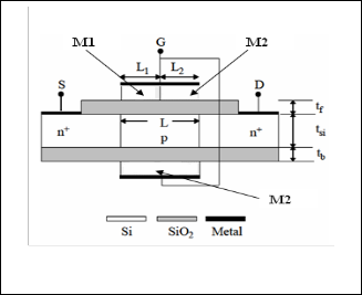
A schematic cross-sectional view of a DMDG FD SON
MOSFET is shown in Fig.1. The front gate consists of dual
2 oxf
dy
y 0
s 2 G 2 , underM2 tf
(6)
materials M1 and M2 of lengths L1 and L2 respectively while
the back gate is material M2. We have used p+ poly as M1 and
n+ poly as M2. Assuming the impurity density in the channel![]()
, where εoxf is the dielectric constant of the oxide (SiO2) at the front gate and tf is the oxide thickness, and
' '
region to be uniform, and neglecting the effect of the fixed
VG1
VGS
VFBfp , VG 2
VGS
VFBfn ,
oxide charges on the electrostatics of the channel, the potential distribution in the silicon thin film before the onset of strong inversion can be written as [8]:
, where VGS is the gate-to-source bias voltage andVFBfp and
VFBfn are the front channel flat-band voltages of the p+ poly and n+ poly respectively and![]()
d 2 x, y d 2
x, y
qN A
(1)![]()
VFBfp M 1
Si ,VFBfn M 2 Si
dx2
dy2
òSi
2. The electric flux at the back gate oxide and back channel
Where Φ (x, y) is the two dimensional potential profile in
the silicon channel, NA is the uniform film doping![]()
interface is continuous for both the materials at the front gate
'
d 1 x, y
εoxb VGSb B
x
, underM1
(7)
concentration independent of the gate length, εSi is the
dy ε t
dielectric constant of silicon, tSi is the film thickness and L is
the device channel length. Considering a second order
potential approximation, Φ (x, y) can be approximated by a
d 2 x, y
y tSi
![]()
Si b
'
oxb GSb B
x
, underM2
(8)![]()
simple parabolic function as proposed by [8].
2
dy
y tSi
εSi tb
(x, y)
s (x)
c1 ( x) y c2 ( x) y (2)
, where εoxb is the dielectric constant of the oxide (here for
Where ΦS (x) is the surface potential, c1 (x) and c2 (x) are x dependent arbitrary coefficients.![]()
DMDG SON, air is taken as the back gate oxide at the front gate and tb is the back oxide thickness, B (x) is the potential function along the back gate oxide -silicon interface, and![]()
'
VGSb
VGS
VFBbn , where VFBbn is the back gate flat-band
voltage and is same as that of VFBfn.
3. At the front gate, the surface potential at the interface of two dissimilar gate materials is continuous.![]()
1 L1 , 0
2 L1 , 0 (9)
![]()
4. At the front gate, the electric flux is continuous at the interface of two different gate materials.
d 1 x, y d 2
x, y
(10)
dx dx
x L1
x L1
Fig. 1. Schematic cross-sectional view of a DMDG FD SON
5. The potential at the source end is
MOSFET.
![]()
1 0, 0
S1 0 Vbi
(11)![]()
Since we have two regions in the front gate of the DMDG structure, the surface potential under M1 and M2 can be written based on (2) as
, where Vbi is the built in potential across the body-source junction.
6. The potential at the drain end is![]()
(x, y)
S1 (x)
c11 (x) y c12 (x) y (3)
![]()
2 L1
L2 , 0
S2 L1 L2
Vbi
VDS
(12)
(x, y)
S 2 (x)
c (x) y c (x) y2 (4)
, where VDS is the applied drain to source voltage.
Where ![]() M1 and
M1 and ![]() M2 are the surface potentials under p+ poly (M1) and n+ poly (M2) respectively,
M2 are the surface potentials under p+ poly (M1) and n+ poly (M2) respectively, ![]() Si is the silicon work function and c11, c12, c21 and c22 are arbitrary coefficients. Depending on the continuity of electrostatic potential, the four boundary conditions used here are as follows:
Si is the silicon work function and c11, c12, c21 and c22 are arbitrary coefficients. Depending on the continuity of electrostatic potential, the four boundary conditions used here are as follows:
1. For dual material gate at the front surface, the electric flux is
The coefficients c11, c12, c21 and c22 are all functions of x and their values are calculated using boundary conditions. Substituting these values in equation (3) and (4) and then in (1), two second order differential equations are obtained as:
IJSER © 2012
International Journal of Scientific & Engineering Research,Volume 3, Issue 6, June-2012 3
ISSN 2229-5518
![]()
![]()
d s1 x dx2
d s 2 x
dx2
α s1
α s 2
x β1 , underM1
x β2 , underM2
(13)
(14)
We have considered a dual material double gate SON![]()
, where
2[1 Cf / CSi
Cf / Cb ]
structure for analytical simulation. The channel length is taken
as 100 nm for the calculations. The different materials that are
t 2 (1 2C / C )
TABLE 1
DIMENTION TABLE
qN A
1
' C f
G1
b
C f
CSi
![]()
' GSb
εSi
2 2CSi
Si C
![]()
2 2CSi
Si C
b b d
' C f C f
G 2 '
qN A
2
Cb CSi
2VGSb
εSi
2 2CSi
Si C
2 2CSi
Si C b
b b
Here CSi is the channel depletion layer capacitance, Cf is the front interface capacitance and Cb is the buried layer (back gate in this case) oxide capacitance. Solving the second order differential equation, we obtain the expressions for surface potential under M1 and M2 of the front gate are given by:![]()
x Aexp ηx Bexp ηx β1
S1 α
![]()
considered for the gate as M1 and M2 are p+ poly and n+ poly respectively. Different parameters that we have used in the calculation are given in table 1.
, for0
![]()
x L1 , underM1
(15)
In Fig.2 the calculated values of surface potential are plotted with respect to the position along the channel of the![]()
β2
S 2 x Cexp η x L1 Dexp η x L1
α
FD DMDG SON for channel length L=100 nm at different drain to source voltages. It is observed that the surface potential at the center exhibits a step function in the surface.![]()
, forL1
, where
x L, underM2
ηL
(16)
Due to this step function, the area under M1 of front gate of the DMDG structure is screened from the drain potential variations. Thus, the step function suppresses the effect of the
A Vbi
![]()
VDS σ2
Vbi
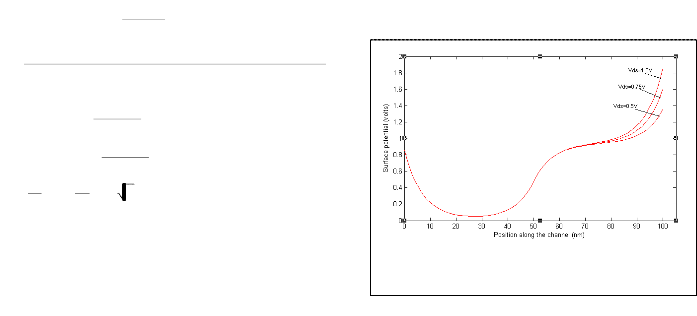
σ1 e
e ηL
electric field induced by the drain-source potential in the
region under M1 and hence, there is no significant change in
the surface potential under M1 as we increase the drain bias.
σ1 σ2
cosh
ηL2
1 e 2 ηL
ηL ηL
B Vbi σ1
Vbi
VDS
σ2 e σ1
1 e 2ηL
σ2 cosh
ηL2 e
C Aexp ηL
σ1 σ2
1 2
D Bexp ηL
σ1 σ2
β1
1 , σ2
1 2
β2 , η α
α α
The electric field variation along the channel length can also be obtained by differentiating the expression of surface potential and can be expressed as
Fig. 2. Variation of Surface potential w.r.t the position in the channel. The parameter Vgs is kept constant and (Vgs = 0.15V)
E1 x Aηexp ηx Bηexp ηx , underM1
(17)
and Vds is varied
E2 x Cηexp η x L1
Dηexp η x L1 , underM2 (18)
This means that drain potential has a very little effect on
IJSER © 2012
International Journal of Scientific & Engineering Research,Volume 3, Issue 6, June-2012 4
ISSN 2229-5518
the drain current after saturation [10] which in turn considera- bly reduces the drain conductance and DIBL effect for the DMDG SON MOSFET.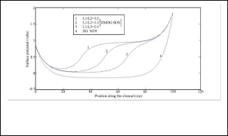
Fig. 3 compares the surface potential profile with respect to channel position for different combinations of gate lengths L1 and L2, keeping the total gate length of the DMDG SON MOSFET to be constant and the surface potential profile with respect to channel position of a DG SON MOSFET. It is seen from the figure that in the second case there is no change in the surface potential but in the first case, the position of mini- mum surface potential, lying under M1 is shifting toward the source as the length of gate M1 is reduced. This causes the peak electric field in the channel to shift more toward the source end and thus there is a more uniform electric field pro- file in the channel. Moreover, it is observed that the channel potential minima for the three cases are not the same. This happens because as L1 increases, the portion of the channel controlled by the gate metal with larger work-function is in- creased.
Fig. 3. Variation of surface potential with position in channel for different combination of gate lengths L1 and L2, keeping the sum (L1 + L2) constant for DMDG and DG SON MOSFET
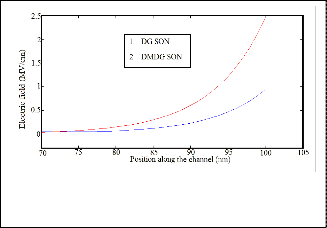
In Fig.4 we have plotted the electric field along the channel length and the nature of electric field variation under M2 is shown. Due to the presence of discontinuity in the surface potential of the DMDG SON MOSFET, the peak electric field near the drain side is substantially reduced for the DMDG devices when compared with that of their DG counterpart. This causes the DMDG devices to achieve simultaneous sup- pression of the short-channel effects and hot-carrier effects.
Fig. 4. Variation of electric field w.r.t the position along the channel under M2. The parameters Vgs and Vds are kept constant (Vgs = 0.15V, Vds = 0.75V).
It is quite evident from the figure that the peak electric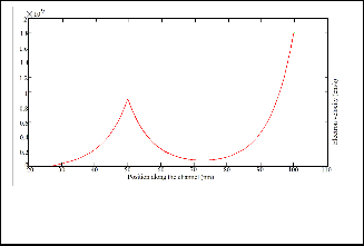
field at the drain end is reduced considerably due to the pres- ence of a gate material with lower work function than the gate material at the source end.
Fig. 5. Variation of electron velocity w.r.t the position along the channel. The parameters Vgs and Vds are kept constant (Vgs =
0.15V, Vds = 0.75V).
In Fig.5, the variation of electron velocity along the chan- nel length has been shown. It is evident from the figure that the nature of the electron velocity distribution resembles that of the electric field distribution in the sub-threshold regime. This type of electron velocity distribution at the source side has an important effect on the overall carrier transport effi- ciency of the DMDG device [11].
Here, we have developed a 2-D analytical model for surface potential and examined the effectiveness of the DMG structure in the front gate of fully depleted SON MOSFETs to suppress Short Channel Effects (SCEs). The results obtained from the analytical model unambiguously establish that the introduction of the DMG structure in the front gate of the fully depleted SON MOSFET leads to subdued SCEs due to a step- function in the channel potential profile at the interface of two materials. The shift in the surface channel potential minima position is negligible with increasing drain biases. Moreover, the peak electric field at the drain end is reduced as compared to that using a single material in the front gate, thus minimizing the hot carrier effect. Thus, the introduction of the DMG structure in the front gate of the fully depleted DG SON MOSFETs improves the short-channel behavior of the SON MOSFETs over their single-material front gate in DG SON and the bulk counterparts.
The authors thankfully acknowledg the financial support obtained from DRDO vide order no. EIRP/ER/1103935M/01/1344 dated 28/06/2011.
[1] S.Deb, N.B.Singh, D.Das, A.K.De, S.K.Sarkar, ―Analytical model of Threshold Voltage and Sub-threshold Slope of SOI and SON MOS- FETs: A comparative study‖, Journal of Electron Devices, Vol. 8, pp. 300-
309, 2010.
IJSER © 2012
International Journal of Scientific & Engineering Research,Volume 3, Issue 6, June-2012 5
ISSN 2229-5518
[2] The International Technology Roadmap for Semiconductor, Emerging
Research Devices, 2009.
[3] M.Current, S.Bebell, I.Malik, L.Feng, F.Henley, ―What is the future of sub-100nm CMOS: Ultrashallow junctions or ultrathin SOI ?‖, Solid State Technology, 2000; 43,.
[4] J.Pretet,S.Monfray,S.Cristoloveanu,T.Skotnicki, ―Silicon-on-Nothing MOSFETs: Performance, Short-Channel Effects, and Backgate Coupl- ing‖, IEEE Transactions on Electron Devices, 2004; 51(2), 240-246.
[5] M.Jurczak,T.Skotnicki,M.Paoli,B.Tormen,J.Martins,J.Regolini, D.Dutartre,P.Roibot,D.Lenoble,R.Pantel,S.Monfray, ―Silicon-on- Nothing (SON)-an Innovative Process for Advanced CMOS‖, IEEE Transactions on Electron Devices, 2000; 47(11), 2179-2187.
[6] T.Sato,H.Nii,M.Hatano,K.Takenaka,H.Hayashi,K.Ishigo,T.Hirano, K.Ida,Y.Tsunashima, ―Fabrication of SON (Silicon on Nothing)- MOSFET and Its ULSI Applications‖, IEIC Technical Re- port,2002;102(178); (SDM2002 66-106);99-104.
[7] D.J.Frank, R.H.Dennard, E.Nowak, D.M.Solomon, Y.Taur, and
H.Wong, ‖Devicescaling limits of Si MOSFETs and their application dependencies‖ , Proc. IEEE, vol.89,pp.259-288, 2001.
[8] G. Venkateshwar Reddy and M. Jagadesh Kumar , ― A New Dual-
Material Double-Gate (DMDG) Nanoscale SOI MOSFET- Two Dimen- sional Analytical Modeling and Simulation, “ IEEE Trans. on Nanotech- nology, Vol. 4, pp.260-268, /March 2005.
[9] A. Chaudhry and M. J. Kumar, "Controlling Short-channel Effects in Deep Submicron SOI MOSFETs for Improved Reliability: A Review", IEEE Trans. on Device and Materials Reliability, Vol.4, pp.99-109, March
2004.
[10] M. J. Kumar and A. Chaudhry, "Two-Dimensional Analytical Model- ing of Fully Depleted Dual-Material Gate (DMG) SOI MOSFET and Evidence for Diminished Short-Channel Effects", IEEE Tran. on Electron Devices, Vol.15, pp.569-574, April 2004.
[11] K. Goel, M. Saxena, M. Gupta, and R. S. Gupta, ―Modeling and simu- lation of a nanoscale three-region tri-material gate stack (TRIMGAS) MOSFET for improved carrier transport efficiency and reduced ho- telectron effects,‖ IEEE Trans. Electron Devices, vol. 53, no. 7, pp.
1623–1633, Jul. 2006.
IJSER © 2012