International Journal of Scientific & Engineering Research, Volume 3, Issue 11, November-2012 1
ISSN 2229-5518
Recent Advances in Nanotechnology
Kuldeep Purohit *, Pooja Khitoliya** and Rajesh Purohit ***
![]()
IJSER © 2012 http://www.ijser.org
International Journal of Scientific & Engineering Research, Volume 3, Issue 11, November-2012 2
ISSN 2229-5518
The nanotechnology refers to a field of applied science and technology whose theme is the control of matter on the atomic and molecular scale, generally 100 nanometers or smaller, and the fabrication of devices or materials that lie within that size range. In the future, "nanotechnology" will likely to include building machines and mechanisms with nanoscale dimensions, referred to these days as Molecular Nanotechnology (MNT). Molecular manufacturing basically emphasizes the use of precisely engineered, computer-controlled nanoscale tools to construct vast numbers of improved tools as well as products with vast numbers of precisely engineered nanoscale features. Recently, the Foresight Institute has suggested an alternate term to represent the original meaning of nanotechnology: Zettatechnology. At the most basic technical level, MNT is building, with intent and design, molecule by molecule, these two things:
Incredibly advanced and extremely capable nano- scale and micro-scale machines and computers,
Ordinary size objects, using other incredibly small machines called assemblers or fabricators (found inside nanofactories)
MNT promises Not just new products but a new means of production; Manufacturing systems that make more manufacturing systems - exponential proliferation; Accelerated product improvement - cheap rapid prototyping; a general-purpose technology; Inexpensive raw materials, potentially negligible capital cost - economic discontinuity; Portable, desktop-size factories - social disruption; in a nutshell, it promises a global transformation.
Nanotechnology is not new to us. The Romans and Chinese
were using nanoparticles thousands of years ago. Similarly, every time we light a match, fullerenes are produced. What is new about nanotechnology is our ability to not only see, and manipulate matter on the nanoscale, but our understanding of atomic scale interactions.
Kuldeep Purohit is pursuing B. Tech. in Electrical Engineering from Indian Institute of Technology, Mandi, (India) E Mail: kuldeeppurohit3@gmail.com
Pooja Khitoliya is pursuing MBA at Indian Institute of
Management (IIM), Calcutta (India).
Dr. Rajesh Purohit is Associate Professor in
Mechanical Engineering Department, Maulana Azad
National institute of Technology, Bhopal, M. P. (India), E Mail: rpurohit73@gmail.com
Manufactured products are made from atoms. The properties of those products depend on how those atoms are arranged. If we rearrange the atoms in coal we can make diamond. If we rearrange the atoms in sand (and add a few other trace elements) we can make computer chips. If we rearrange the atoms in dirt, water and air we can make potatoes.
As an analogy to all this we can say that Nanotechnology helps us snap together the fundamental building blocks of nature easily, inexpensively and in most of the ways permitted by the laws of physics.
The term, "nanotechnology," was proposed by K. Eric Drexler. Technically speaking, Nanotechnology refers to a field of applied science and technology whose theme is the control of matter on the atomic and molecular scale, generally 100 nanometers or smaller, and the fabrication of devices or materials that lie within that size range
Interest in nanotechnology is strong because standard silicon techniques have nearly reached their limit-CPUs and similar products can’t get much smaller with current technology because manufacturers can’t keep stuffing more and more transistors in the same space. However nanotechnology may allow this. We could develop a new manufacturing technology, which will let us inexpensively build computer systems with mole quantities of logic elements that are molecular in both size and precision and are interconnected in complex and highly idiosyncratic patterns.
There are two concepts commonly associated with nanotechnology:
Positional assembly
Massive parallelism
Positional assembly helps to get the right molecular parts in the right places and massive parallelism helps to keep the costs down.
Nanostructures are made by Lithography and Self- assembly- Physical or chemical. Lithography is a top-down fabrication technique where a bulk material is reduced in size to nanoscale pattern.
The concept of molecular self-assembly prepares small molecules of almost any structure and assembles these
IJSER © 2012 http://www.ijser.org
International Journal of Scientific & Engineering Research, Volume 3, Issue 11, November-2012 3
ISSN 2229-5518
single molecules into supramolecular assemblies consisting
of many molecules arranged in a well defined manner. They automatically arrange themselves into some useful conformation through a bottom-up approach.
In nanomanufacturing we are integrating "bottom up" self- assembly with "top down" lithography called Hierarchical Manufacturing.
In order to understand the unusual world of nanotechnology, we need to get an idea of the units of measurement involved. A nanometer (nm) is one-billionth of a meter, smaller than the wavelength of visible light. To put that scale in context, the comparative size of a nanometer to a meter is the same as:
->10 times the diameter of a hydrogen atom, or
-> That of a marble to the size of the earth.
One nanometer is still large compared to the atomic scale. An atom has a diameter of about 0.1 nm. An atom's nucleus is much smaller -- about 0.00001 nm. Atoms are the building blocks for all matter in our universe. Nature has perfected the science of manufacturing matter molecularly. For instance, our bodies are assembled in a specific manner from millions of living cells. Cells are nature's nanomachines. At the atomic scale, elements are at their most basic level. On the nanoscale, we can potentially put these atoms together to make almost anything. The nanoscale is more interesting than the atomic scale because the nanoscale is the first point where we can assemble something - it's not until we start putting atoms together that we can make anything useful.
At nanoscale the role of quantum mechanics statistical mechanical effects, comes into play. The rules of quantum mechanics are very different from classical physics, which means that the behavior of substances at the nanoscale can sometimes contradict common sense. This effect does not come into play by going from macro to micro dimensions. However, it becomes dominant when the nanometer size range is reached. Additionally, a number of physical
(mechanical, electrical, optical, etc.) properties also change
when compared to macroscopic systems. Also an increase in surface area to volume ratio, at nanoscale; alters the mechanical, thermal and catalytic properties of materials. For example, due to an increase in surface area , Melting points can change, opaque substances become transparent (copper); inert materials become catalysts (platinum); stable materials turn combustible (aluminum); solids turn into liquids at room temperature (gold); insulators become conductors (silicon). A material such as gold, which is chemically inert at normal scales, can serve as a potent chemical catalyst at nanoscales.
Nanomaterials are materials with morphological features smaller than a one tenth of a micrometre in at least one dimension. Nanomaterials exhibit unique physical and electrochemical properties, thereby enabling the manufacture of stronger, harder, more wear-resistant materials. Interface and Colloid science has given rise to many materials which may be useful in nanotechnology, such as carbon nanotubes, other fullerenes, various nanoparticles and nanorods. Members of the fullerene family are a major subject of research falling under the nanotechnology umbrella.
Bottom-up approach:
In the "bottom-up" approach, materials and devices are built from molecular components which assemble themselves chemically by principles of molecular recognition. Simply put, these seek to arrange smaller components into more complex assemblies.
Top-down approach:
In the "top-down" approach, nano-objects are constructed from larger entities without atomic-level control. Or simply put, these seek to create smaller devices by using larger ones to direct their assembly.
IJSER © 2012 http://www.ijser.org
International Journal of Scientific & Engineering Research, Volume 3, Issue 11, November-2012 4
ISSN 2229-5518
Ingredients like zinc oxide can leave a white shine
behind. But sunscreens with zinc oxide nanoparticles rub on clear.
enhance clothing. By coating fabrics with a thin layer of zinc oxide nanoparticles, manufacturers can create clothes that give better protection from UV radiation. Some clothes have nanoparticles in the form of little hairs or whiskers that help repel water and other materials, making the clothing stain-resistant.
that adding aluminum silicate nanoparticles to scratch- resistant polymer coatings made the coatings more effective, increasing resistance to chipping and scratching. Scratch-resistant coatings are common on everything from cars to eyeglass lenses.
the nano-systems as well as polymer conjugation. Together
these drug delivery systems would not only improve drug administration and the efficiency and safety of conventional chemotherapies, but also revolutionize the pharmaceutical and biomedical industries in cancer therapies (Orive, et al., 2005).
6.9 Some new products: New products incorporating nanotechnology are coming out every day. Wrinkle- resistant fabrics, deep-penetrating cosmetics, liquid crystal displays (LCD) and other conveniences using nanotechnology have already been developed. Before long, we'll see dozens of other products that take advantage of nanotechnology ranging from Intel microprocessors to bio- nanobatteries, capacitors only a few nanometers thick.
7.1 Carbon nanotubes (CNTs): They are allotropes of carbon with a nanostructure that can have a length-to- diameter ratio greater than one lakh. These cylindrical carbon molecules have novel properties that make them potentially useful in many applications in nanotechnology, electronics, optics and other fields of material science, as well as potential uses in architectural fields. They exhibit extraordinary strength and unique electrical properties and are efficient conductors of heat. Inorganic nanotubes have also been synthesized. Their name is derived from their size, since the diameter of a nanotube is in the order of a few nanometers (approximately 1/50,000th of the width of a human hair), while they can be up to several millimeters in length. The nature of the bonding of a nanotube is described by applied quantum chemistry, specifically, orbital hybridization. The chemical bonding of nanotubes is composed entirely of sp2 bonds, similar to those of graphite. This bonding structure, which is stronger than the sp3 bonds found in diamonds, provides the molecules with their unique strength. Nanotubes naturally align themselves into "ropes" held together by Van der Waals forces. Under high pressure, nanotubes can merge together, trading some sp² bonds for sp³ bonds, giving the possibility of producing strong, unlimited-length wires through high- pressure nanotube linking.
Types of carbon nanotubes are as follows: Single-walled, Multi-walled, Fullerite, Torus, Nanobud, and Nanoflower. The strength and flexibility of carbon nanotubes makes them of potential use in controlling other nanoscale structures, which suggests they will have an important role in nanotechnology engineering. CNTs find applications in
IJSER © 2012 http://www.ijser.org
International Journal of Scientific & Engineering Research, Volume 3, Issue 11, November-2012 5
ISSN 2229-5518
structures, electrical circuits, drug delivery vessels, Sola8r. Optical clarity in comparison to conventionally
cells, Ultra capacitors etc.
Carbon nanotubes have been intensively explored for biological and biomedical applications in the past few years. Ultra sensitive detection of biological species with carbon nanotubes can be realized after surface passivation to inhibit the non-specific binding of biomolecules on the hydrophobic nanotube surface. Electrical nanosensors based on nanotubes provide a label-free approach to biological detection. Surface-enhanced Raman spectroscopy of carbon nanotubes opens up a method of protein microarray with detection sensitivity down to 1 fmol/L. In vitro and in vivo toxicity studies reveal that highly water soluble and serum stable nanotubes are biocompatible, nontoxic, and potentially useful for biomedical applications. In vivo biodistributions vary with the functionalization and possibly also with size of nanotubes, with a tendency to accumulate in the reticuloendothelial system (RES), including the liver and spleen, after intravenous administration. If well functionalized, nanotubes may be excreted mainly through the biliary pathway in feces. Carbon nanotube-based drug delivery has shown promise in various In vitro and in vivo experiments including delivery of small interfering RNA (siRNA), paclitaxel and doxorubicin. Moreover, single- walled carbon nanotubes with various interesting intrinsic optical properties have been used as novel photoluminescence, Raman, and photoacoustic contrast agents for imaging of cells and animals. Further multidisciplinary explorations in this field may bring new opportunities in the realm of biomedicine (Liu et al., 2009).
Mechanical properties e.g. strength, modulus and dimensional stability.
Decreased permeability to gases, water and hydrocarbons.
Thermal stability and heat distortion temperature. Flame retardancy and reduced smoke emission. Chemical resistance.
Surface appearance. Electrical conductivity.
filled polymers.
Several orders of magnitude of change in resistance are observed upon chemical doping and dedoping of the conducting polymer polyaniline. This large conductivity range can be utilized to make sensitive chemical sensors. Polyaniline, in its nanofiber form, has even greater sensing capabilities due to the small fiber diameters, high surface area, and porous nanofiber network that enhance gas diffusion into the fibers. Polyaniline nanofiber composite materials can be used to enhance detection of analytes that unmodified polyaniline would not otherwise be able to detect (Virji et al., 2009).
Improvements in mechanical property have resulted in major interest in nanocomposite materials in numerous automotive, industrial and general applications. These include potential application for mirror housings on various vehicles, door handles, engine covers, intake manifolds and timing belt covers. More general applications currently being considered include applications as impellers and blades for vacuum cleaners, power tool housings, mower hoods and covers for portable electronic equipment such as mobile phones, pagers etc.
8.1 Energy harvesting for self-powered nanosystems:
There are energy harvesting technologies other than the well-known solar cell and thermoelectrics that have potential for powering nanosystems. The piezoelectric nanogenerators are developed using aligned ZnO nanowire arrays. This is a potential technology for converting mechanical movement energy (such as body movement, muscle stretching, blood pressure), vibration energy (such as acoustic/ultrasonic wave), and hydraulic energy (such as
IJSER © 2012 http://www.ijser.org
International Journal of Scientific & Engineering Research, Volume 3, Issue 11, November-2012 6
ISSN 2229-5518
flow of body fluid, blood flow, contraction of blood vessel,
dynamic fluid in nature) into electric energy for self- powered nanosystems. A key advantage of nanodevices and nanosystems is that they usually operate at a very low power in the range from nW to W. As a result, the energy harvested from the environment may be sufficient to power the system. Biochemical power sources are mechanical energy, vibrational energy, chemical energy (glucose), and hydraulic energy. If a small fraction of such energy could be converted into electricity, the energy may be sufficient to power small devices for biomedical applications (Wang,
2008).
Extreme ultraviolet lithography will use mirrors to direct light with a wavelength of 13nanometers to print features at 32-nanometer scale. The smaller scale will yield chips that run much faster.
Lithium ion batteries using multiwalled nanotubes are safer and more effective, with up to 10 times life and 5 times the available power are already available in the market.
Quantum dots-semiconductor crystals that are just a few nanometers wide- provide the needed precision for Blu-ray and HD DVD blue lasers.
Obviously, there would be significant advantages of materials that are 100 times stronger than present materials. Objects made from these materials could be up to 100 times lighter, using 100 times less of quantity of substance. By substituting diamondoid composite material this factor could be increased to about 250. As a result, ultra light cars, trucks, trains, aircraft, and spacecraft would use far less energy, especially with atomically smooth surfaces to reduce internal friction and air resistance losses. Space transportation costs could be reduced considerably with use of the products of nanotechnology.
It is a hollow solid structure, with diameter in the 1-1000 nanometer range, which can be filled with anticancer drugs and detection agents. Targeting moieties can also be attached to the surface. Nanovectors can be used for targeted gene therapy. Liposome is a type of nanovector made of lipids surrounding a water core (Ferrari, 2005).
They are among the leading approaches under development for the early detection of precancerous and malignant lesions from biological fluids. These and other nanodevices can provide essential breakthroughs in the fight against cancer (Ferrari, 2005).
"Micellar nanocontainers" or "Micelles" are nanoscale
polymeric containers that could be used to selectively deliver hydrophobic drugs to specific sites within individual cells.
materials due to their novel shape- and size-dependent chemical and physical properties that differ drastically from their bulk counterparts. Nanoscale crystals are often harder, stronger and more wear resistant than the same materials in bulk form. Nanocrystals might be used to make super-strong and long-lasting metal parts. The crystals also may be added to plastics and other metals to make new types of composite structures for automotive, electronics and other applications.
Emergence and development of nanoscience and nanotechnology brings new opportunities to the applications of nanocrystals as nanocatalysts. The excellent catalytic properties of nanomaterials have been attributed to the large surface area to their small size. Some experimental results demonstrate that exposure of specific crystal planes of nanocrystals is indeed an essential factor in determining their catalytic performance (Wang, Xie and Li, 2009). Fig.1 shows the first atomic-scale image of nanocrystals that helps reduce pollution, having a surprising triangular, rather than hexagonal, shape. The new information should help researchers improve the chemical process.
Fig. 2 shows a single-electron transistor (SET), which is a three terminal device, where single electron current between a source and a drain through a nanocrystal is controlled by a gate. The nanocrystals are the tiny light spectacles.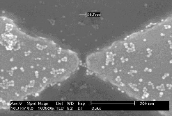
IJSER © 2012 http://www.ijser.org
International Journal of Scientific & Engineering Research, Volume 3, Issue 11, November-2012 7
ISSN 2229-5518
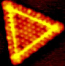
Fig. 1 The first atomic-scale images of nanocrystals
Fig. 2 Single-electron transistor (SET)
nanotube) types, with an irregular horn-like shape, may be a critical component of new generation fuel cells. The main characteristic of the carbon nanohorns is that when many of the nanohorns group together, an aggregate (a secondary particle) of about 100 nanometers is created. The advantage being, that when used as an electrode for a fuel cell, not only the surface area is extremely large, but also, it is easy for the gas and liquid to permeate to the inside. In addition, the nanohorns are easily prepared with high purity as compared with normal nanotubes and therefore it is expected to become a low-cost raw material.
dimensional structures, with unique electrical and optical properties, that are used as building blocks in nanoscale devices. Stripped or 'superlatticed' nanowires can function as transistors, LEDs (light-emitting diodes) and other optoelectronic devices, biochemical sensors, heat-pumping thermoelectric devices, or all of the above, along with the same length of wire.
Speculation is that they "may someday make highly sensitive magnetic field detectors, perhaps finding application in hard drive read heads. Alternatively,
nanosprings could serve as positioners, or even as tiny
conventional springs, for nanomachines in the future.
Silica nanosprings are novel nanostructured material for hydrogen storage. Hydrogen storage for transportation applications remains a challenge. Current approaches are still short of published goals, in particular in being able to operate at acceptable temperatures. Silica nanosprings can store and release hydrogen non-dissociatively at room temperature. The potential of nanosprings for hydrogen storage was initially demonstrated by exposing the mats to hydrogen and measuring chemical shifts using X-ray photoelectron spectroscopy (Norton et al., 2009).
and the other polymeric nanoscale fibers (made from polymers). They are currently used in air and liquid filtration applications. Using a process called "electrospinning" - or e-spin - a polymer "mesh" is formed into a nanofiber membrane, hence "nanomesh", with 150 -
200 nm diameters. Some of them have been made since
1970, but were not called "nano" until recently. One potential use is "to prevent body tissues from sticking together as they heal. They also break down in the body over time like biodegradable sutures.
Vapor grown carbon fibers are obtained as shown in Fig. 3. The diameters of these fibres can vary from 100 nm to 500 nm. Fig. 4 shows scanning electron micrograph of Ultra- Web(R) nanofibers.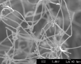
Fig. 3 SEM of vapor grown carbon fibres;
IJSER © 2012 http://www.ijser.org
International Journal of Scientific & Engineering Research, Volume 3, Issue 11, November-2012 8
ISSN 2229-5518
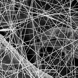
Fig. 4 Ultra-Web(R) nanofiber produced on a SEM
built filters, sensors, or diffraction gratings to make them function better. As activated carbon may also be used as an alternate fuel storage medium, due to its massive internal surface area, scientists believe nanopores, tiny holes that allow DNA to pass through one strand at a time, will make DNA sequencing more efficient. In biology, they are complex protein assemblies that span cell membranes and allow ionic transport across the otherwise impermeable lipid bilayer. Nanopores are important because while some pores help maintain cell homeostasis, others disrupt cell function. A nanopore can be a protein channel in a lipid bilayer or an extremely small isolated 'hole' in a thin, solid- state membrane such that DNA and RNA, can be registered and characterized singly.
for the separation of molecules, such as proteins or DNA, for research in genomics. Another is as masks to prevent exposure to biological pathogens such as viruses that can be as small as 30 nanometers in diameter.
is analogous to using a quill pen but on a billionth scale, and it may transform dip-pen nanolithography. It allows for drawing electronic circuits a thousand times smaller than current ones. The "pen" is an atomic force microscope (AFM).
be used as nanopens for controlled chemical delivery or removal from regions as small as 100 nanometers. They can
also be used as vessels for containing molecules whose
optical properties change in response to their chemical environment. Other uses include controlled chemical etching with the precision of atomic force microscopy, chemical imaging of surfaces, delivering femtosecond laser pulses, and performing NSOM/SNOM imaging using a UV excimer laser.
that can draw patterns of tiny lines just 30 molecules thick and a single molecule high and produces eight identical patterns at once and extends. Dip-pen nanolithography is a step towards mass production of nanoscale devices and circuits by converting what was a serial process to a parallel one. This may be used to miniaturize electronic circuits, pattern precise arrays of organic and biomolecules such as DNA and put thousands of different medical sensors on an area much smaller than the head of a pin.
between 0.1 to 10 micrometers. They are also called nanodots, nanocrystals and quantum beads. Impregnating fluorescent crystal chips into these beads allows simultaneous measurement of thousands of biological interactions, a stepping stone for breakthroughs in the diagnosis and treatment of disease with the potential to accelerate drug discovery and clinical diagnostics.
the world's smallest guitar is 10 micrometers long, about the size of a single cell, with six strings each about 50 nanometers or 100 atoms wide. Figure 5 shows a Nanoguitar.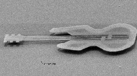
Fig. 5 Smallest guitar, about the size of a human blood cell, carved out of crystalline silicon
IJSER © 2012 http://www.ijser.org
International Journal of Scientific & Engineering Research, Volume 3, Issue 11, November-2012 9
ISSN 2229-5518
intense study. The studies have also revealed about the
surprising electron and hole mobilities of the order 104 cm2/Vs. This has raised a possibility of using grapheme itself as a device similar to CNTs. However, being zero-gap semiconductor, it cannot be directly used in the applications like field-effect Transistors (FETs). However, besides the 2D confinement, grapheme ribbons can be further confined by forming narrower ribbons, which would result in a split of original 2D energy into several 1D modes. Depending on the boundary conditions, some sets of these 1D modes do not pass through the intersection point of the conduction and valence band, and these quasi-
1D graphene ribbons become semiconductors with a finite energy gap [8].
Thus formed GNRs would possess properties, which are quite different from those of graphene. These GNRs can be utilized in the applications related to transistors too. Typically, a 20nm ribbon can carry confinement-induced gap of the order of 30 meV.
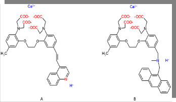
XNOR logic gate (absorption) AND logic gate
XOR logic gate (transmittance)
Fig. 6 Molecular logic gates
Working of gates: The working of Compund-A requires the two cations- Ca++ and H+ as the chemical inputs to the logic gate. When both of them are absent, the chromophore shows maximum absorbance in the wavelength region Ultra Violet/Visible at 390nm. On introduction of Calcium ion in the solution, “BlueShift” occurs and absorbance at
390nm decreases. Likewise introduction of proton causes a “Red Shift” and hence, the absorbance at 390nm decreases. When both cations are present, net results stays to be highest absorbance at 390nm. The compound-B exhibits fluorescence only when both the cations are present in the solution and therefor the system represents an AND logic gate.
Similarly, many other compounds have successfully been found to act as various logic gates, some are still under work, as they form an approximate picture, but perfection is yet to be achieved.
IJSER © 2012 http://www.ijser.org
International Journal of Scientific & Engineering Research, Volume 3, Issue 11, November-2012 10
ISSN 2229-5518
exist. Because of their potential utility in simple arithmetic
these molecular machines are also called moleculators.
Single molecule transistor technology (which has similar research status) has got scope in chemical and biological sensing. DNA-based logic gates that could carry out calculations inside the body have been constructed for the first time. The work brings the prospect of injectable biocomputers programmed to target diseases as they arise. “The bio-computer would sense biomarkers and immediately react by releasing counter-agents for the disease.”
Apocalyptic Goo: Eric Drexler, the man who introduced the word nanotechnology, presented a frightening apocalyptic vision -- self-replicating nanorobots malfunctioning, duplicating themselves a trillion times over, and rapidly consuming the entire world as they pull carbon from the environment to build more of themselves. It's called the "grey goo" scenario, where a synthetic nano-size device replaces all organic material. Another scenario involves nanodevices made of organic material wiping out the Earth
- the "green goo" scenario.
There are some hefty social concerns about nanotechnology. Nanotechnology may also allow us to create more powerful weapons, both lethal and non-lethal. Thus we should examine carefully all the possibilities of nanotechnology before designing increasingly powerful weapons.
There are some ethical issues also. If nanotechnology in medicine makes it possible for us to enhance ourselves physically, is that ethical? In theory, medical nanotechnology could make us smarter, stronger and give us other abilities ranging from rapid healing to night vision. Should we pursue such goals? Could we continue to call ourselves human, or would we become transhuman - the next step on man's evolutionary path? Since almost every technology starts off as very expensive, would this mean we'd create two races of people - a wealthy race of modified humans and a poorer population of unaltered people? We don't have answers to these questions, but several organizations are urging nanoscientists to consider these implications now, before it becomes too late.
Some issues deal with the world of finance and economics. If molecular manufacturing becomes a reality, how will that impact the world's economy? Assuming we can build anything we need with the click of a button, what happens to all the manufacturing jobs? If you can create anything using a replicator, what happens to currency? Would we
move to a completely electronic economy? Would we even
need money?
Thus, the power and potential of nanotechnology must be harnessed with utmost caution and with the sole aim of benefiting the human race.
1. By taking advantage of quantum-level properties, Molecular Nanotechnology MNT allows for unprecedented control of the material world, at the nanoscale, providing the means by which systems and materials can be built with exacting specifications and characteristics.
2. The use of Nanotechnology is continuously transforming daily use products, making consumer goods plentiful, inexpensive and highly durable.
3. The medicine will take a quantum leap forward, with the use of nanotechnology.
4. Single molecule transistor technology has got scope in chemical and biological sensing. DNA-based logic gates that could carry out calculations inside the body have been constructed for the first time.
5. Space travel and colonization will become safe and affordable with the advances that nanotechnology is bringing in aerospace materials.
6. With continuous use of nanotechnology, the global life styles will change radically.
7. The nanotechnology will have a drastic impact on the human behavior and society.
1. Orive, G., Hernandez, R.M., Gascon, A.R. and Pedraz, J.L. (2005) ‘Micro and nano drug delivery systems in cancer therapy’, Cancer Therapy, Vol.3, pp.131-138.
2. Liu, Z., Tabakman, S., Welsher, K. and Dai, H. (2009) ‘Carbon nanotubes in biology and medicine: In vitro and in vivo Detection, Imaging and Drug Delivery’, Nano Research, Vol. 2, pp.85-120.
3. Virji, S., Kojima, R., Fowler, J.D., Villanueva, J.G.,
Kaner, R.B. and Weiller, B.H. (2009) ‘Polyaniline Nanofiber Composites with Amines: Novel Materials for Phosgene Detection’, Nano Research, Vol. 2, No. 2, pp.135-142.
IJSER © 2012 http://www.ijser.org
International Journal of Scientific & Engineering Research, Volume 3, Issue 11, November-2012 11
ISSN 2229-5518
4. Wang, Z.L. (2008) ‘Energy Harvesting for Self-
Powered Nanosystems’, Nano Research, Vol. 1, pp.1-8.
5. Ferrari, M. (2005) ‘Cancer Nanotechnology:
Opportunities and Challenges’, Nature Reviews
Cancer, Vol. 5, pp.161-171.
6. Wang, D., Xie, T. and Li, Y. (2009) ‘Nanocrystals: Solution-Based Synthesis and Applications as Nanocatalysts’, Nano Research, Vol. 2, pp.30-46.
7. Norton, M.G., McIlroy, D.N., Corti, G., Miller, M.A. (2009) ‘Silica Nanosprings – A Novel Nanostructured Material for Hydrogen Storage’, Nanotech Conference and Expo, May 3-7, 2009, Houston, Texas, US.
8. Zhihong Chen, Yu-Ming Lin, Michael J. Rooks, Phaedon Avouris (2007), ‘Graphene nano-ribbon electronics’, IBM T. J. Watson Research Center, Yorktown Heights, NY 10598, USA.
9. Vladimir V. Mitin, Viatcheslav A. Kochelap, Michael A. Stroscio (2007), ‘Introduction to Nanoelectronics’, Cambridge University Press.
IJSER © 2012 http://www.ijser.org