International Journal of Scientific & Engineering Research, Volume 4, Issue 12, December-2013 926
ISSN 2229-5518
Quad Squares Center Circular Slotted Microstrip
RFID Applications Antenna
Akash Porwal, Dr. Neelam Srivastava
Abstract— Quad squares center circular slotted, orthogonal slits and corner truncated novel patch structure are proposed for circularly polarized (CP) Ultra High frequency (UHF) Radio Frequency Identification (RFID) applications. The structure constitutes 0.27λ x 0.27λ x 0.0137λ at 900 MHz ground plane and FR-4 Epoxy substrate. The proposed antenna provides the Return loss S 11 (dB) of -39.11 dB with 887 MHz – 932 MHz Bandwidth range typi- cally 45 MHZ covering wide Ultra High Frequency (UHF) range, minimum Axial Ratio of 0.7741 dB at 910.7 MHZ and VSW R < 2 is simulated using Elec- tromagnetic High Frequency structure simulator (HFSS). The single coaxial feeded patch Gain and Bandwidth is tuned via electromagnetically coupled parasitic patch with peak gain of about 4dB. The slits and truncated corners reduce the antenna size with circularly polarized (CP) radiation over low cost FR-4 Epoxy substrate.
Index Terms— Axial Ratio (AR), Circular polarization (CP), Circularly Polarized Microstrip Antenna (CPMA), Radio Frequency Identification (RFID), Gain
Bandwidth Tuning (GBT), High Frequency Structure Simulator (HFSS), Slotted patch (SP).
1 INTRODUCTION
—————————— ——————————
IJSER
he Radio Frequency identification (RFID) is a wireless data transmission and reception technique for tracking
and identifying an object that employs the world wide fre- quency span of 840 MHz - 960 MHz. The technique configura- tion involves a Reader, a Tag and a data processing system. The reader is typically a trans-receiver that transmits and re- ceives the modulated RF signal scattered from the Tag. The circular Polarized (CP) radiation is desirable due to random orientation of the Tag, as the circularly polarized microstrip antennas (CPMAs) reduce the losses caused by the multipath effects and thus making system more efficient and reliable. With the enhancing technology good gain, highly directive, good impedance match, compact geometry, low cost reader
————————————————
• Akash Porwal is currently pursuing masters degree program in Microelectronics from Institute of Engineering and Technology Lucknow, Gautam Buddh Technical University, INDIA.
E-mail: porwalakash.1989@gmail.com
• Dr. Neelam Srivastava Professor (Electronics Engineering Dept.) Institute of Engineering and Technology Lucknow, Gau- tam Buddh Technical University, INDIA.
E-mail: neelam.srivastava@ietlucknow.edu
antennas that can be mounted on multiple surfaces are desira- ble for the applications such as electronic toll collections, assest identification, access control etc. However introduction with sensory systems enlarges the application areas including environment monitoring and health care applications etc. While designing the antenna Bandwidth i.e. the frequency range of operation with constant gain achievement is the prior consideration. Several techniques developed such as stacking patches over single, double or multi-layer, introduction of multi-layer dielectric substrate or meta- material, introduction of metallic plates inside the dielectric substrate that forms mu- tual coupling have been reported in literature so far that pro- vide a reliable way of tuning the gain and Bandwidth of de- sign. However the use of parasitic patch generates electro- magnetic coupling between the main patch i.e. (patch fed by coax probe) and the patch that is in free space is one easy way to obtain good Gain-Bandwidth results. The relatively thicker substrate prevents the surface wave generation results in good gain achievement. In this paper novel quad squares, center
circular slotted, orthogonal slits and corner truncated patch
IJSER © 2013 http://www.ijser.org
International Journal of Scientific & Engineering Research, Volume 4, Issue 12, December-2013 927
ISSN 2229-5518
structure is simulated. All the squares slots are asymmetric in
size and relative center positions to each other. The corner truncations and orthogonal slits reduce the patch size with operational frequency band and Axial ratio tuning for Circu- larly Polarizes (CP) radiation is presented. The parasitic patch introduced is of similar size of the main patch to improve the Gain-Bandwidth. The geometry is simulated using the elec- tromagnetic ANSOFT High Frequency structure simulator (HFSS) with operating Frequency of 900 MHz using low cost FR-4 Epoxy dielectric substrate.
2 ANTENNA CONFIGURATIONS
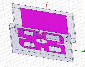
The cross section view of the proposed Quad squares, center circular slotted microstrip patch antenna is shown in fig.1 (a) and patch in excitation in fig.1 (b).
embedded orthogonal slits length LS = 15mm and width WS =
5mm respectively.
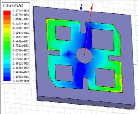
Fig.1 (b) patch in Excitation.
The coax probe impedance is 50 ohms which is randomly lo-
cated at position (-15mm, 0mm) from center. The electromag- netic coupled patch is of same main patch dimensions without slots at height 25.428mm from the main patch over the FR-4
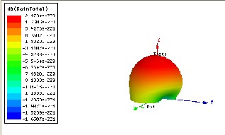
Epoxy substrate with height of h = 5mm. the simulated Return Loss S11 (dB) , Axial Ratio , minimum and maximum Gain val- ues at the bore sight are represented in fig.2 (a) – (c). The total Bandwidth of around 45 MHz with minimum Axial Ratio of
0.7741 dB is achieved. The peak Gain obtained is 3.91 dB.
Fig.1 (a) cross section view
The length of square patch is L = 68mm and ground plane size of antenna is 90mm X 90mm. The coaxial feed point from the center is (-15mm, 0mm). The dielectric FR-4 Epoxy substrate height H1 = 4.572mm, dielectric constant = 4.4 and loss tangent
= 0.002. The center circular slot radius R= 16mm. The top right square i.e. first quadrant slot length L1 = 18mm, top left square i.e. second quadrant slot length L2 = 12mm, bottom left square i.e. third quadrant slot length L3 = 14mm and bottom right
square i.e. fourth quadrant slot length L4 = 16mm. The
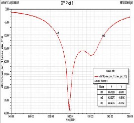
Fig.2 (a) Return Loss S11 (dB) plot.
IJSER © 2013 http://www.ijser.org
International Journal of Scientific & Engineering Research, Volume 4, Issue 12, December-2013 928
ISSN 2229-5518
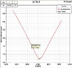
Fig.2 (b) Axial ratio plot.
The proposed antenna found reliable in countries like Singa- pore, Australia, Taiwan, Korea, Hong Kong, China, and Amer- ica and covers the majority world wide RFID i.e. Radio Fre-
3 PARAMETRIC ANALYSIS
3.1 EFFECT OF SLIT LENGTH
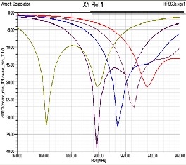
Fig.3 (a) Return Loss S11 (dB) Plot.
The fig.3 (a) represents the Return Loss S11 (dB) variation for length LS and width WS tuning of the orthogonally located
IJSER
quency Identification range.
slits. The slit length LS = 15mm and width WS = 5mm provides
the Return Loss S11 (dB) of -39.1 dB with frequency band of operation around 900 MHz. The variation step size taken to be 2.5 mm in slit length LS. The slit tuning provides the desired Frequency of operation.
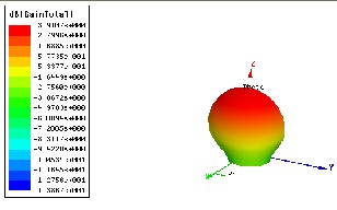
Fig.2 (c) min. and max. Gain values.
Table 1
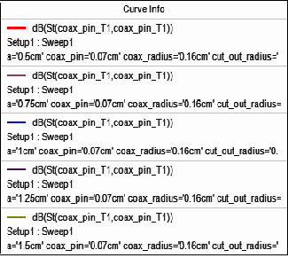
Parametric Configuration
IJSER © 2013 http://www.ijser.org
International Journal of Scientific & Engineering Research, Volume 4, Issue 12, December-2013 929
ISSN 2229-5518
3.2 EFFECT OF DIELECTRIC HEIGHT
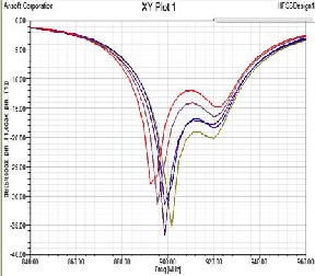
Fig.3 (b) Return Loss S11 (dB) Plot.
The larger dielectric height improves the Antenna Gain by
4 CONCLUSION
The proposed antenna performance characteristics are adequate for the Ultra High frequency (UHF) Radio Frequen- cy Identification (RFID) applications with high Bandwidth that covers majority worldwide Frequency span. The para- sitic patch improves the Gain- Bandwidth relationship of the configuration. The slits and corner truncations improves the Return Loss S11 (dB) and is about -39.11 dB and minimum axial ratio 0.771 dB for circularly Polarized (CP) radiation. The sim- ulated antenna found applications in countries like Singapore, Australia, Taiwan, China, America and Hong Kong. While considering cost as prior value use of low cost FR-4 Epoxy is suitable dielectric material for the design. The slots and corner
truncations reduce the patch size in quiet good ratio.
IJSER
reducing surface wave generation and thus improves the Re-
turn Loss S11 (dB). The dielectric height of 4.572mm provides the best result for the configuration mentioned with Return Loss S11 (dB) of -39.11 dB respectively as shown in figure. 3(b). The variation step size taken here is 3mm.
Table 2
Parametric Configuration
REFERENCES
[1] Nasimuddin, Senior Member, IEEE, Zhi Ning Chen, Fellow, IEEE, and Xianming Qing, Member, IEEE “ Asymmetric- Circular Shaped Slotted Microstrip An- tennas for Circular Polarization and RFID Applica- tions.” IEEE TRANSACTIONS ON ANTENNAS AND PROPOGATION VOL. 58, NO. 12, DECEMBER
2010.
[2] Zhongbao Wang, Shaojun Fang, Shiqiang Fu, and Mujie Fan “Single-Fed Single-Patch Broadband Circu- larly Polarized Antenna for UHF RFID Reader Appli- cations” 2010 2nd International Conference on Indus- trial and Information Systems 978-1-4244-8217-
7/10/$26.00 ©2010 IEEE.
[3] N. Gautam* (1), P. Deo (2), A. Mehta(1), D. Mirshekar- Syahkal(2), P.J. Massey and H. Nakano(3) “Circularly Polarized Square Patch Antenna with Square Slots for RFID Reader Applications.”978-1-4244-4968-
2/10/$25.00 ©2010 IEEE.
IJSER © 2013 http://www.ijser.org
International Journal of Scientific & Engineering Research, Volume 4, Issue 12, December-2013 930
ISSN 2229-5518

[4] Donghai Yu, Yao Ma, Zhiyun Zhang, Renjie Sun “A
Circularly Polarized Aperture-coupled Patch Antenna for RFID Reader.” 978-1-4244-2108-4/08/$25.00 © 2008
IEEE.
[5] Abdi K.H. Obsiye, Hany E. AbdEl-Raouf, and Rafique El-Islam” Modified Printed Crescent Patch Antenna For Ultrawideband RFID (UWB-RFID) Tag” 2008
IEEE INTERNATIONAL RF AND MICROWAVE CONFERENCE PROCEEDINGS December 2-4, 2008, Kuala Lumpur, MALAYSIA.
[6] Nasimuddin, Karu P. Esselle, and A. K. Verma “Wideband High-Gain Circularly Polarized Stacked Microstrip Antennas with an Optimized C-Type Feed and a Short Horn” IEEE TRANSACTIONS ON AN-
TENNAS AND PROPAGATION, VOL. 56, NO. 2,

AKASH PORWAL- Presently Microelec- tronics M.Tech scholar (Institute of Engineering and Technolo- gy, Lucknow). He received the B.Tech degree in Electronics and Communication Engineering in year 2011 from Gautam Buddh Technical University Lucknow, INDIA. His research interest includes Microstrip Antennas, Channel coding and Microelectronics.
Dr. (Prof.) NEELAM SRIVASTAVA - She
FEBRUARY 2008.
IJSEreceived BE ElecRtronics Engineering from M.M.M. Engineer-
[7] Yanun Liu'*, Mahmoud Shahabadi*, Safieddin Safavi-
Naeini', Shady Suleiman Gain “Improvement of an Array of Sequentially Rotated Circularly Polarized Microstrip Antennas Using Stacked Parasitic Patches”
0-7803-7846-61031971.2003 IEEE.
[8] P. C. Sharma and K. C. Gupta, “Analysis and opti- mized design of single feed circularly polarized mi- crostrip antennas,” IEEE Trans. Antennas Propag., vol. 29, pp. 949–955, 1983.
[9] Pei-Ju Lin, Hsien-Chiao Teng and Yu-Jung Huang, Ming-Kun Chen “Design of Patch Antenna for RFID Reader Applications”.
ACKNOWLEDGMENT
The author wishes heartiest thanks and regards to Mr. Ranjan Kumar (Indian Institute of Technology Kanpur U.P, INDIA Project Associate) for his help and full support regarding
completion of the research.
ing College Gorakhpur, M.Tech in Microwave Engineering
from IT/BHU Varanasi and Ph.d in Optical Networks from IET, Lucknow from Lucknow University. Her research field includes Antenna Design, Digital Communication and Chan- nel coding etc.
IJSER © 2013 http://www.ijser.org